DOI:
10.1039/D2NA00929C
(Paper)
Nanoscale Adv., 2023,
5, 2190-2198
Effects of drying time on the formation of merged and soft MAPbI3 grains and their photovoltaic responses†
Received
19th December 2022
, Accepted 2nd March 2023
First published on 2nd March 2023
Abstract
The grain sizes of soft CH3NH3PbI3 (MAPbI3) thin films and the atomic contact strength at the MAPbI3/P3CT-Na interface are manipulated by varying the drying time of the saturated MAPbI3 precursor solutions, which influences the device performance and lifespan of the resultant inverted perovskite photovoltaic cells. The atomic-force microscopy images, cross-sectional scanning electron microscopy images, photoluminescence spectra and absorbance spectra show that the increased short-circuit current density (JSC) and increased fill factor (FF) are mainly due to the formation of merged MAPbI3 grains. Besides, the open-circuit voltage (VOC) of the encapsulated photovoltaic cells largely increases from 1.01 V to 1.15 V, thereby increasing the power conversion efficiency from 17.89% to 19.55% after 30 days, which can be explained as due to the increased carrier density of the MAPbI3 crystalline thin film. It is noted that the use of the optimized drying time during the spin coating process results in the formation of merged MAPbI3 grains while keeping the contact quality at the MAPbI3/P3CT-Na interface, which boosts the device performance and lifespan of the resultant perovskite photovoltaic cells.
Introduction
Solution-processed perovskite crystalline thin films have been widely used in various applications, such as photovoltaic cells,1–3 light-emitting diodes,4–6 photo-detectors,7–9 memory devices10–12 and field-effect transistors,13–15 mainly due to their tunable crystal structure and superior optoelectronic properties.16–18 Organometal trihalide perovskites are suitable for solar cells as the light absorbing layer owing to the large absorption coefficient, moderate refractive index, small exciton binding energy and long carrier diffusion length,19–21 which results in a high power conversion efficiency (PCE) of 25.6% (25.0%) when the regular-type (inverted-type) structure is used.22,23 In the lead trihalide perovskite photovoltaic cells, the size of the multi-crystalline grains was increased from several hundred nanometers to several micrometers in order to reduce the defect density at the grain boundaries of the light absorbing layer.24–26 However, the larger grain (lower surface area) corresponds to the lower doping concentration of the perovskite crystalline thin film, thereby resulting in the lower open-circuit voltage (VOC) of the resultant cells.27–29 In other words, the ideal VOC of the intrinsic perovskite based photovoltaic cells is related to the Fermi levels of the electron transport layer (ETL) and hole transport layer (HTL).30–32 In recent years, the power conversion efficiency (PCE) of the perovskite photovoltaic cells can be higher than 20% when the grains of the light absorbing layer are sub-micrometer size,33–35 which means that the defects at the grain boundaries are effectively passivated, thereby resulting in low carrier recombination (high fill factor). In other words, there is an optimal grain size of the perovskite crystalline thin films in the highly efficient and stable perovskite photovoltaic cells. In the highly efficient and stable perovskite photovoltaic cells, the grain sizes of the light absorbing layer are ranging from 300 nm to 500 nm,22,23,33–35 which is slightly larger than the size of the surface feature in the ITO thin film.36,37 It is noted that the layered structure is a common feature of these perovskite grains,38 which indicates that the sub-micrometer-sized particles are single-crystalline grains.39 In other words, the optimized size of perovskite grains is highly related to the size of the surface feature in the ITO thin film. On the other hand, the residual solvent molecules in the solution-processed perovskite grain thin films degrade the device performance and lifespan of the resultant photovoltaic cells,40–42 which indicates the importance of the drying process during the formation of high-quality perovskite thin films.
In this study, the main aim is to investigate the effects of the perovskite grain size on the device performance of the P3CT-Na HTL based inverted perovskite photovoltaic cells with a facile encapsulation method.43 Our experimental results show that the re-dissolving process of perovskite nucleation can be used to manipulate the grain size of the perovskite crystalline thin films which strongly influences the VOC and lifespan of the encapsulated perovskite photovoltaic cells.
Experiments
Poly[3-(4-carboxybutyl)thiophene-2,5-diyl] (P3CT) and NaOH were purchased from Matrix Scientific and Sigma-Aldrich, respectively. The regioregularity of the used P3CT polymers is about 85%. PbI2 and CH3NH3I (MAI) were purchased from Uni-Onward and Lumtec, respectively. Phenyl-C61-butyric acid methyl ester (PCBM) and (bathocuproine) BCP were purchased from Uni-Onward and Sigma-Aldrich, respectively. Dimethylformamide (DMF), dimethyl sulfoxide (DMSO), chlorobenzene (CB) and bromobenzene (BrB) were purchased from Sigma-Aldrich. Isopropyl alcohol (IPA) was purchased from ACROS. The preparation of P3CT-Na/water solution, MAPbI3/DMF:DMSO solution, PCBM/CB:BrB solution and BCP/IPA solution is illustrated in our previous report.44 The P3CT-Na solution, perovskite precursor (1.5 M) solution, PCBM/CB:BrB solution (2 wt%) and BCP/IPA (0.089 wt%) solution were stirred at 500 rpm for 3 h at room temperature.
The device structure is Ag/BCP:PCBM/MAPbI3/P3CT-Na/ITO/glass. Ag and ITO are used as the cathode and anode, respectively. PCBM and P3CT-Na are used as the electron transport layer (ETL) and hole transport layer (HTL), respectively. BCP is used to modify the PCBM thin film and the contact quality at the PCBM/MAPbI3 interface.45 A MAPbI3 crystalline thin film is used as the light absorbing layer. The ITO/glass (7 Ω sq−1) substrates were modified by using a UV–ozone cleaner for 45 minutes in order to increase the surface wettability. The P3CT-Na polymer modification layer, 500 nm-thick MAPbI3 crystalline thin film, and 60 nm-thick PCBM thin film were fabricated by using the spin coating method. Besides, the BCP/IPA solution treatment was used to modify the PCBM thin film and the contact quality at the PCBM/MAPbI3 interface. The 100 nm-thick Ag thin film was fabricated by using the vacuum thermal evaporation method. The detailed information of the device fabrication process is illustrated in our previous report.44 The fabrication conditions of the P3CT-Na polymer ultra-thin layer, MAPbI3 crystalline thin film, PCBM thin film and Ag thin film are described in the ESI.† After the injection of CB into the MAPbI3 precursor solution, the precursor turns from a transparent solution to a light brown solution, thereby forming nucleation sites and/or intermediate states. In other words, the residual spin period can be viewed as the drying time of the MAPbI3 precursor solution. During the spin coating process of the MAPbI3 precursor solution, the spin time in the second step was changed from 29 s to 49 s in order to vary the drying times from 20 s to 40 s. The active area of a single MAPbI3 photovoltaic device is defined to be 2 × 5 mm2 by using a metallic shadow mask during the thermal evaporation process of Ag thin films. Each sample contains four cells. One glass substrate and one Parafilm were used to encapsulate the device in order to increase the device lifespan. The encapsulation method is described in Fig. S1.† The current density–voltage (J–V) curves of the inverted perovskite photovoltaic cells were obtained by using a source-meter system (NI-USB 6356 DAQ) under one sun illumination (AM1.5G, 100 mW cm−2). The light intensity of the light-emitting diode based solar simulator (VeraSol-2, Newport) was calibrated by using a reference cell (91150V, Newport) before the J–V curve measurement.
To investigate the trends of the VOC, JSC and FF, MAPbI3/P3CT-Na/ITO/glass samples with and without encapsulation were prepared. An atomic force microscope (UTEK, Nanoview 1000) and field-emission scanning electron microscope (JEOL, JSM-7600F) were used to obtain the surface morphologies and cross-sectional images of the samples, respectively. An X-ray diffractometer (Bruker, D8 Advance) was used to characterize the crystal structures of the samples. A home-made optical spectrometer was used to measure the absorbance and reflectance spectra. The setup of the absorbance/reflectance spectrometer is illustrated in Fig. S2.† A home-made optical microscope based photoluminescence (PL) spectrometer46 was used to analyze the light emissions of the samples under top excitation and bottom excitation.
Results and discussion
Fig. 1 presents the J–V curves of the inverted perovskite photovoltaic cells under one sun illumination (AM 1.5G, 100 mW cm−2). The photovoltaic performance of the 8 cells for each condition is listed in Table 1. The average VOC increases from 1.010 V to 1.017 V with the increase in the drying time from 20 s to 40 s, which means that a longer drying time results in a lower potential loss. When the drying time increases from 20 s (30 s) to 30 s (40 s), the average JSC increases (decreases) from 19.01 mA cm−2 (22.25 mA cm−2) to 22.25 mA cm−2 (20.32 mA cm−2), which means that the drying time largely influences the contact quality at the MAPbI3/P3CT-Na interface, thereby dominating the collection efficiency of photo-generated holes.47 The photovoltaic cells were encapsulated with a facile method on the 2nd day in order to increase the device lifespan.43 It is noted that the VOC values increased after the encapsulation process. When the drying time is 20 s, the JSC and FF are both increased after the encapsulation process. When the drying time is 30 s or 40 s, the JSC and FF are both decreased after the encapsulation process, thereby slightly decreasing the PCE on the 2nd day. Besides, the VOC hysteresis of the encapsulated solar cells largely increases from 0.033 V to 0.220 V with the increase in the drying time from 30 s to 40 s (see Fig. S3†), which can be used to explain the lower VOC and FF when the drying time is 40 s. On the 80th day, the VOC and JSC values are both increased while maintaining the high FF values. The slightly decreased FF is mainly due to the increased series resistance (RS). Fig. 2 presents the J–V curves of the inverted perovskite photovoltaic cells on the 2nd day and 80th day. The VOC and JSC values of the encapsulated photovoltaic cells are both increased, which means that the encapsulation process increases (reduces) the exciton dissociation efficiency (potential loss). When the drying time is 20 s or 30 s, an s-shape characteristic can be observed in the J–V curves, which means that an ultra-thin potential barrier may be formed at the PCBM/MAPbI3 interface.48 In other words, it is possible to form a large-bandgap HPbI3 interlayer49 in between the PCBM and MAPbI3 thin films due to the formation of MA+-PCBM-MA+ cations,50 as shown in Fig. 3. The formation of a MA+-PCBM-MA+ cation produces two H+ ions via dehydrogenation from the two MA+ cations. Then, it is possible to form a HPbI3 interlayer when the H+ ions migrate to MA+ vacancies. It is noted that the s-shape characteristics are not observed in the J–V curves when the drying time is 40 s. Fig. 4 presents the day-dependent device performance of the best perovskite photovoltaic cells under one sun illumination. After encapsulation, the photovoltaic cells have similar trends in the day-dependent VOC, JSC and FF. When the drying time is 30 s, the VOC (FF) of the encapsulation photovoltaic cell largely increases (slightly decreases) from 1.087 V (78.1%) to 1.156 V (72.6%), thereby maintaining the average PCE to be higher than 17.5% within 80 days. On the 80th day, the higher average PCE of the encapsulated cells is mainly due to the higher average VOC when the drying time is 30 s. And, the differences in average VOC values are higher than the standard deviation values of VOC (see Table 1), which can be used to confirm that the PCE and device lifespan of the resultant perovskite photovoltaic cells are better when the drying time is 30 s. To analyze the day-dependent device performance, the VOC curves and FF curves are fitted with an exponential growth function and a linear decay function, respectively (see Fig. S4†). The rising time values of the VOC curves (decay rates of the FF curves) are 11.59 days (−0.0015 per day), 19.83 days (−0.0008 per day) and 18.03 days (−0.0012 per day) when the drying times are 20, 30 and 40 s, respectively. The trend of the VOC rising time values is inversely proportional to the trend of the FF decay rate values, which is probably related to the shallow defect density in the MAPbI3 crystalline thin films and the formation rate of MA+-PCBM-MA+ cations and a large-bandgap HPbI3 interlayer at the PCBM/MAPbI3 interface. The existence of shallow defects does not significantly influence the exciton binding energy of perovskite crystalline thin films.43,51 In other words, the high VOC of 1.156 V can be explained as due to the formation of shallow defects in the soft MAPbI3 crystalline thin film.52 To confirm the stable JSC values, the incident photon-to-current conversion efficiency (IPCE) spectra of the encapsulated cells were measured on the 406th day, as shown in Fig. S5(a).† Fig. S5(b)† shows that the integrated current density values are about 22 mA cm−2 which is close to the stable JSC values. It is noted that the highest PCE is lower than 20%, which is probably due to the lower regioregularity of the used P3CT polymers.47
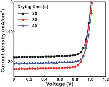 |
| | Fig. 1 Current density–voltage (J–V) curves of the photovoltaic cells under one sun illumination (AM 1.5G, 100 mW cm−2). MAPbI3 perovskite films are prepared with different drying times. | |
Table 1 Day-dependent device performance of photovoltaic cells under one sun illumination (AM 1.5G, and 100 mW cm−2)
| Day/encapsulation |
Drying time (s) |
V
OC (V) |
J
SC (mA cm−2) |
FF (%) |
PCE (%) |
R
s (Ω) |
| 1st/no |
20 |
1.010 ± 0.001 |
19.01 ± 0.36 |
73.2 ± 5.3 |
14.05 ± 1.32 |
38 ± 1 |
| 1st/no |
30 |
1.015 ± 0.001 |
22.25 ± 0.32 |
78.5 ± 0.4 |
17.72 ± 0.37 |
39 ± 1 |
| 1st/no |
40 |
1.017 ± 0.001 |
20.32 ± 0.45 |
72.5 ± 6.5 |
14.98 ± 1.72 |
50 ± 5 |
| 2nd/with |
20 |
1.043 ± 0.014 |
19.34 ± 0.04 |
75.1 ± 3.0 |
15.15 ± 0.85 |
58 ± 17 |
| 2nd/with |
30 |
1.086 ± 0.001 |
20.00 ± 0.27 |
76.6 ± 1.5 |
16.63 ± 0.58 |
40 ± 1 |
| 2nd/with |
40 |
1.045 ± 0.034 |
19.89 ± 0.31 |
70.1 ± 5.9 |
14.57 ± 1.99 |
48 ± 10 |
| 80th/with |
20 |
1.109 ± 0.022 |
21.24 ± 0.17 |
72.8 ± 1.9 |
17.15 ± 0.94 |
98 ± 36 |
| 80th/with |
30 |
1.133 ± 0.023 |
21.82 ± 0.05 |
71.9 ± 0.7 |
17.78 ± 0.57 |
112 ± 13 |
| 80th/with |
40 |
1.092 ± 0.020 |
21.81 ± 0.26 |
68.5 ± 2.5 |
16.31 ± 1.11 |
152 ± 32 |
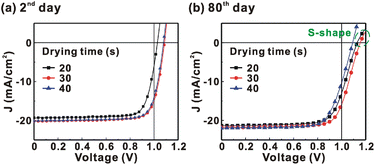 |
| | Fig. 2 Current density–voltage (J–V) curves of the photovoltaic cells with a facile encapsulation method under one sun illumination (AM 1.5G and 100 mW cm−2). MAPbI3 perovskite films are prepared with different drying times. (a) 2nd day; (b) 80th day. | |
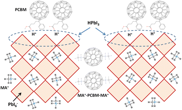 |
| | Fig. 3 Formation of MA+-PCBM-MA+ cations and an HPbI3 interlayer. | |
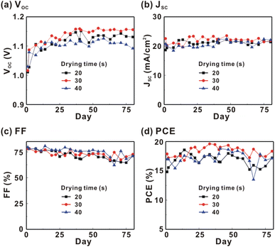 |
| | Fig. 4 Day-dependent device performance of the photovoltaic cells under one sun illumination (AM 1.5G and 100 mW cm−2). MAPbI3 perovskite films are prepared with different drying times. (a) VOC; (b) JSC; (c) FF; (d) PCE. | |
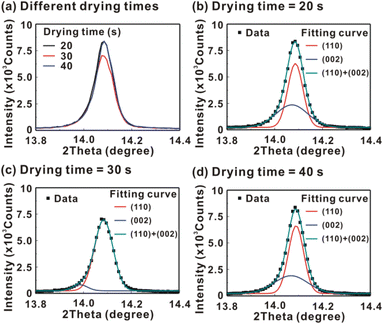
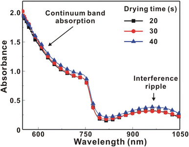
Fig. 5 presents the atomic force microscopy (AFM) images and cross-sectional scanning electron microscopy (SEM) images of the MAPbI3/P3CT-Na/ITO/glass samples fabricated with different drying times. When the drying time increases from 20 s to 40 s, the trend of the average surface roughness values (Fig. 5(a)–(c)) is proportional to the trend of the grain sizes (see Fig. 5(d)–(f)). In other words, the longer drying time results in merged MAPbI3 grains, thereby increasing the surface roughness which can be calculated from the AFM images. It is noted that the MAPbI3 crystalline thin film is separated from the substrate when the drying time is 30 s or 40 s, which means that the formation of merged MAPbI3 grains reduces the atomic contact strength at the MAPbI3/P3CT-Na interface, thereby leading to mechanical stress induced separation during the splitting process. In other words, there is a trade-off between the MAPbI3 grain size and the contact quality at the MAPbI3/P3CT-Na interface, which dominates the trends of the JSC values and FF values of the resultant inverted perovskite photovoltaic cells on the first day (see Table 1). Besides, the trend of the grain sizes is proportional to the trend of the VOC values and the s-shape characteristics in the J–V curve of the resultant inverted perovskite photovoltaic cells on the first day (see Table 1) due to the recued potential loss at grain boundaries.53,54 The trend of the grain sizes also influences the formation of s-shape characteristic in the J–V curves on the 80th day (see Fig. 2(b)), which means that the larger grains (less grain boundaries) result in less MA+-PCBM-MA+ cations, thereby reducing the formation of a HPbI3 barrier at the PCBM/MAPbI3 interface. Fig. 6(a) presents the main X-ray diffraction patterns of the MAPbI3/P3CT-Na/ITO/glass samples fabricated with different drying times. The asymmetric curve indicates that the (110)-oriented peak and (002)-oriented peak overlapped.55 To separate the diffraction features of the two peaks, the asymmetric peaks are fitted with a two-Gaussian function. The fitting results are plotted in Fig. 6(b)–(d). The peak intensity values, the diffraction angles of peaks and the intensity ratio between the two peaks are listed in Table 2. The trend of the peak intensity values is inversely proportional to the trend of the (002)-peak position values, which is related to the lattice distortion of the MAPbI3 crystalline thin films. As shown in Fig. 6(c), the diffraction angle of the (002) peak is shorter than the others, which means that the crystal plane distance along the (002) direction is longer than the others when the drying time is 30 s. In a (110)-oriented MAPbI3 thin film, the (002) crystal plane is parallel to the inter-grain surface. In other words, the longer crystal plane distance along the (002) direction can be explained due to the tensile stress from the interfacial contact and the formation of merged grains. Besides, the intensity ratio of the (110)-peak and (002)-peak (I110/I002) is the highest value (14.58) when the drying time is 30 s. In other words, the crystal orientation of the merged MAPbI3 grains is also related to the surface properties of the P3CT-Na/ITO/glass substrate, thereby forming the (110) preferred MAPbI3 crystalline thin film.56Fig. 7 presents the top-excited PL spectra of the MAPbI3/P3CT-Na/ITO/glass samples fabricated with different drying times. The trend of the PL intensities is proportional to the trend of the I110/I002 ratio values (see Table 2). When the drying time is 30 s, the PL intensity from the top region of the MAPbI3 crystalline thin film corresponds to the highest value. When the drying time is reduced to 20 s, the relatively lower PL intensity can be explained as due to the higher defect density at the inter-gain boundaries of the MAPbI3 crystalline thin film. When the drying time is extended to 40 s, the relatively lower PL intensity can be explained as due to the higher surface defect density of the rough MAPbI3 crystalline thin film. Fig. 8 presents the absorbance spectra of the MAPbI3/P3CT-Na/ITO/glass samples fabricated with different drying times. In the near-infrared wavelength range from 800 nm to 1050 nm, the formation of ripples is due to the thin-film interference between interfaces. The larger amplitude of the interference ripple indicates the weaker light scattering from the surface due to the lower roughness of the MAPbI3 thin films.57,58 The trend of the ripple amplitudes is inversely proportional to the trend of the Ra values (see Fig. 5). Besides, the higher absorbance is due to the larger Ra when the drying time is 40 s. In general, the slope of the absorbance curve in the continuum absorption band is inversely proportional to the exciton binding energy of the MAPbI3 crystalline thin film.59 It is noted that the trend of the exciton binding energies is inversely proportional to the trends of the JSC values and FF values (see Table 1). In other words, the higher PCE of the inverted perovskite photovoltaic cells is also related to the lower exciton binding energy of the MAPbI3 crystalline thin film due to the formation of merged and soft perovskite grains.
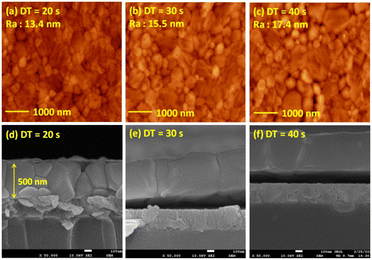 |
| | Fig. 5 Atomic-force microscopy (AFM) images and scanning electron microscopy (SEM) images of MAPbI3/P3CT-Na/ITO/glass samples fabricated with different drying times (DTs). (a) AFM, DT = 20 s; (b) AFM, DT = 30 s; (c) AFM, DT = 40 s; (d) SEM, DT = 20 s; (e) SEM, DT = 30 s; (f) SEM, DT = 40 s. | |
 |
| | Fig. 6 (a) Main X-ray diffraction patterns of the MAPbI3/P3CT-Na/ITO/glass samples fabricated with different drying times (DTs). (b) Fitting curves, DT = 20 s; (c) fitting curves, DT = 30 s; (d) fitting curves, DT = 40 s. | |
Table 2 Key features in the main XRD patterns, PL spectra and absorbance spectra of the MAPbI3/P3CT-Na/ITO/glass sample. MAPbI3 films are prepared with different drying times
| Drying time |
XRD peak intensity (counts) |
2θ of the 002-peak (degree) |
2θ of the 110-peak (degree) |
Ratio of I(110)/I(002) |
PL peak intensity (counts) |
Slope of the absorbance curve (1/nm) |
| 20 s |
8141 |
14.072 |
14.086 |
1.36 |
48 |
−0.0097 |
| 30 s |
6809 |
13.985 |
14.085 |
14.58 |
67 |
−0.0105 |
| 40 s |
8141 |
14.070 |
14.090 |
1.72 |
38 |
−0.0088 |
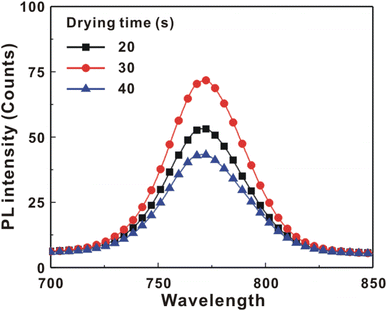 |
| | Fig. 7 Top-excited photoluminescence spectra of the MAPbI3/P3CT-Na/ITO/glass samples fabricated with different drying times. | |
 |
| | Fig. 8 Absorbance spectra of the MAPbI3/P3CT-Na/ITO/glass samples fabricated with different drying times. | |
Fig. 9 presents the reflectance spectra and bottom-excited PL spectra of the MAPbI3/P3CT-Na/ITO/glass samples before and after the encapsulation process. The MAPbI3 crystalline thin films are fabricated with different drying times. The reflectance peak is related to the exciton transition of the MAPbI3 crystalline thin film. According to the material dispersion relation, a longer exciton transition wavelength results in a longer reflectance peak wavelength due to the higher refractive index.60 Therefore, the difference between the reflectance peak wavelength and the PL peak wavelength (Δλ = λPL − λR) is proportional to the Stokes shift (exciton binding energy). The reflectance peak wavelengths, PL peak wavelengths and Δλ values of the MAPbI3/P3CT-Na/ITO/glass samples are listed in Table 3. Before encapsulation, the trend of the Δλ (exciton binding energy) values is proportional to the trend of the grain sizes (see Fig. 5(d)–(f)), which means that the formation of merged and soft grains results in lattice distortion, thereby increasing the Δλ (exciton binding energy) in the bottom region of the MAPbI3 crystalline thin film.61 In other words, the extended drying time results in a distorted lattice in the bottom region of the MAPbI3 crystalline thin film, thereby decreasing the atomic contact strength at the MAPbI3/P3CT-Na interface (see Fig. 5(d) and (e)). In the aspect of the device performance of un-encapsulated photovoltaic cells on the first day, the average VOC value increases from 1.010 V to 1.017 V with the increase in the drying time from 20 s to 40 s, which can be explained due to the increased grain size (decreased potential loss). However, the average JSC (FF) value has the highest value when the drying time is 30 s, which is due to the better contact quality at the MAPbI3/P3TC-Na interface and the lower exciton binding energy of the MAPbI3 thin film.
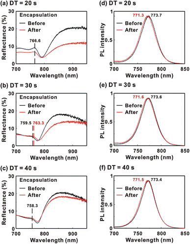 |
| | Fig. 9 Reflectance and photoluminescence (PL) spectra of the MAPbI3/P3CT-Na/ITO/glass samples before and after encapsulation. MAPbI3 films are fabricated with different drying times (DTs). (a) Reflectance, DT = 20 s; (b) reflectance, DT = 30 s; (c) reflectance, DT = 40 s; (d) PL, DT = 20 s; (e) PL, DT = 30 s; (f) PL, DT = 40 s. | |
Table 3 Reflectance peak wavelength and PL peak wavelength of the MAPbI3/P3CT-Na/ITO/glass samples before encapsulation, after encapsulation and after 10 days. MAPbI3 films are fabricated with different drying times
| Encapsulation |
Drying time |
Reflectance peak wavelength, λR (nm) |
PL peak wavelength, λPL (nm) |
Δλ = λPL − λR (nm) |
| Before |
20 s |
766.6 |
773.7 |
7.1 |
| Before |
30 s |
759.5 |
773.6 |
14.1 |
| Before |
40 s |
758.3 |
773.4 |
15.1 |
| After |
20 s |
766.6 |
771.3 |
4.7 |
| After |
30 s |
763.3 |
771.6 |
8.3 |
| After |
40 s |
758.3 |
771.5 |
13.2 |
After encapsulation, the decreased Δλ values are 2.4, 5.8 and 1.9 nm when the drying times are 20, 30 and 40 s, respectively. It is noted that the trend of the decreased Δλ (exciton binding energy) values is proportional to the trend of the increased VOC values (see Table 1) after encapsulation. The decreased Δλ (exciton binding energy) in the bottom region of the MAPbI3 crystalline thin film can be explained as due to the formation of shallow defects after the encapsulation process, which increases the effective Fermi level for electrons of the soft MAPbI3 crystalline thin film, thereby resulting in the higher VOC of the inverted perovskite photovoltaic cells.
Conclusions
In summary, the open-circuit voltage of the inverted perovskite crystalline photovoltaic cells can be largely increased from 1.010 V to 1.156 V via the formation of merged and soft CH3NH3PbI3 (MAPbI3) grains and the reduced exciton binding energy (increased carrier density), which are confirmed by analyzing the surface morphologies, cross-sectional images, crystal structures and excitonic properties of the MAPbI3/P3CT-Na/ITO/glass samples with and without encapsulation. It is noted that the photovoltaic cells maintain the average power conversion efficiency to be higher than 17.5% within 80 days when the MAPbI3 thin film is fabricated with an optimized drying time of 30 s.
Conflicts of interest
There are no conflicts to declare.
Acknowledgements
Financial support was provided by the Ministry of Science and Technology (Taiwan) under Grants MOST 110-2112-M-033-008-MY3 and MOST 111-2112-M-033-008.
References
- J. Y. Kim, J.-W. Lee, H. S. Jung, H. Shin and N.-G. Park, High-efficiency perovskite solar cells, Chem. Rev., 2020, 120, 7867–7918 CrossRef CAS PubMed.
- J. Zhang, W. Zhang, H.-M. Cheng and S. P. P. Silva, Critical review of recent progress of flexible perovskite solar cells, Mater, Today, 2020, 39, 66–88 CAS.
- M. Jost, L. Kegelmann, L. Korte and S. Albrecht, Monolithic perovskite tandem solar cells: A review of the present status and advanced characterization methods toward 30% efficiency, Adv. Energy Mater., 2020, 10, 1904102 CrossRef CAS.
- Y. Shen, M.-N. Li, Y. Li, F.-M. Xie, H.-Y. Wu, G.-H. Zhang, L. Chen, S.-T. Lee and J.-X. Tang, Rational interface engineering for efficient flexible perovskite light-emitting diodes, ACS Nano, 2020, 14, 6107–6116 CrossRef CAS PubMed.
- X.-K. Liu, W. Su, S. Bai, Y. Jin, J. Wang, R. H. Friend and F. Gao, Metal halide perovskites for light-emitting diodes, Nat. Mater., 2021, 20, 10–21 CrossRef CAS PubMed.
- C.-C. Lee, J. Iskandar, A. K. Akbar, H.-M. Cheng and S.-W. Liu, Controllable crystallization based on the aromatic ammonium additive for efficiently near-infrared perovskite light-emitting diodes, Org. Electron., 2021, 99, 106327 CrossRef CAS.
- C. Bao, J. Yang, S. Bai, W. Xu, Z. Yan, Q. Xu, J. Liu, W. Zhang and F. Gao, High performance and stable all-inorganic metal halide perovskite-based photodetectors for optical communication applications, Adv. Mater., 2018, 30, 1803422 CrossRef PubMed.
- H. Jing, R. Peng, R.-M. Ma, J. He, Y. Zhou, Z. Yang, C.-Y. Li, Y. Liu, X. Guo, Y. Zhu, D. Wang, J. Su, C. Sun, W. Bao and M. Wang, Flexible ultrathin single-crystalline perovskite photodetector, Nano Lett., 2020, 20, 7144–7151 CrossRef CAS PubMed.
- Z. Lan, L. Cai, D. Lu and F. Zhu, Narrowband near-infrared perovskite/polymer hybrid photodetectors, ACS Appl. Mater. Interfaces, 2021, 13, 981–988 CrossRef CAS PubMed.
- C. Gu and J.-S. Lee, Flexible hybrid organic-inorganic perovskite memory, ACS Nano, 2016, 10, 5413–5418 CrossRef CAS PubMed.
- Z. Xu, Z. Liu, Y. Huang, G. Zheng, Q. Chen and H. Zhou, To probe the performance of perovskite memory devices: defects property and hysteresis, J. Mater. Chem. C, 2017, 5, 5810–5817 RSC.
- X. Wu, H. Yu and J. Cao, Unraveling the origin of resistive switching behavior in organolead halide perovskite based memory devices, AIP Adv., 2020, 10, 085202 CrossRef CAS.
- H. Peng, J. Guo, G. Chen and W. Qin, Self-powered perovskite CH3NH3PbBr3 field effect transistor with fast response and high sensitivity in sensing, Mater. Today, 2021, 12, 100185 CrossRef CAS.
- B. Jeong, L. Veith, T. J. A. M. Smolders, M. J. Wolf and K. Asadi, Room-temperature halide perovskite field-effect transistors by ion transport mitigation, Adv. Mater., 2021, 33, 2100486 CrossRef CAS PubMed.
- H. Zhu, A. Liu, K. I. Shim, H. Jung, T. Zou, Y. Reo, H. Kim, J. W. Han, Y. Chen, H. Y. Chu, J. H. Lim, H.-J. Kim, S. Bai and Y.-Y. Noh, High-performance hysteresis-free perovskite transistors through anion engineering, Nat. Commun., 2022, 13, 1741 CrossRef CAS PubMed.
- W.-J. Yin, T. Shi and Y. Yan, Unique properties of halide perovskites as possible origins of the superior solar cell performance, Adv. Mater., 2014, 26, 4653–4658 CrossRef CAS PubMed.
- L. M. Herz, Charge-carrier mobilities in metal halide perovskites: Fundamental mechanisms and limits, ACS Energy Lett., 2017, 2, 1539–1548 CrossRef CAS.
- L. Chouhan, S. Ghimire, C. Subrahmanyam, T. Miyasaka and Y. Biju, Synthesis, optoelectronic properties and applications of halide perovskite, Chem. Soc. Rev., 2020, 49, 2869–2885 RSC.
- S. H. Chang, K.-F. Lin, C.-H. Chiang, S.-H. Chen and C.-G. Wu, Plasmonic structure enhanced exciton generation at the interface between the perovskite absorber and copper nanoparticles, Sci. World J., 2014, 2014, 128414 Search PubMed.
- F. Ruf, M. F. Ayguler, N. Ciesbrecht, B. Rendenbach, A. Magin, P. Docampo, H. Kalt and M. Hetterich, Temperature-dependent studies of exciton binding energy and phase-transition suppression in (Cs,FA,MA)Pb(I,Br)3 perovskites, APL Mater., 2019, 7, 031113 CrossRef.
- Y. Liu, Z. Yang and S. F. Liu, Recent progress in single-crystalline perovskite research including crystal preparation, property evaluation, and applications, Adv. Sci., 2018, 5, 1700471 CrossRef PubMed.
- J. Jeong, M. Kim, J. Seo, H. Lu, P. Ahlawat, A. Mishra, Y. Yang, H. A. Hope, F. T. Eickemeyer, M. Kim, Y. J. Yoon, I. W. Choi, B. P. Darwich, S. J. Choi, Y. Jo, Y. H. Lee, B. Walker, S. M. Zakeeruddin, L. Emsley, U. Rothlisberger, A. Hagfeldt, D. S. Kim, M. Gratzel and J.-Y. Kim, Pesudo-halide anion engineering for α-FAPbI3 perovskite solar cells, Nature, 2021, 592, 381–385 CrossRef CAS PubMed.
- Z. Li, B. Li, X. Wu, S. A. Sheppard, S. Zhang, D. Gao, N. J. Long and Z. Zhu, Organometallic-functionalized interfaces for highly efficient inverted perovskite solar cells, Science, 2022, 376, 416–420 CrossRef CAS PubMed.
- H. Li, G. Wu, W. Li, Y. Zhang, Z. Liu, D. Wang and S. F. Liu, Additive engineering to grow micron-sized grains for stable high efficiency perovskite solar cells, Adv. Sci., 2109, 6, 1901241 CrossRef PubMed.
- G. Lu, W. Zhu, F. He, D. Chen, C. Zhang and Y. Hao, Enhanced sensitivity of grain sizes to precursor stoichiometry enables high-quality CH3NH3PbI3 films for efficient perovskite solar cells, Mater. Lett., 2019, 250, 88–91 CrossRef CAS.
- M. Nukunudompanich, G. Budiutama, K. Suzuki, K. Hasegawa and M. Ihara, Dominant effect of the grain size of the MAPbI3 perovskite controlled by the surface roughness of TiO2 on the perovskite of perovskite solar cells, CrystEngComm, 2022, 22, 2718–2727 RSC.
- S. H. Chang, K.-F. Lin, H.-M. Cheng, C.-C. Chen, W.-T. Wu, S.-H. Chen and C.-G. Wu, Influence of organic cations on high-performance CH3NH3PbI3 based photovoltaics, Sol. Energy Mater. Sol. Cells, 2016, 145, 375–381 CrossRef CAS.
- C.-C. Chen, S. H. Chang, L.-C. Chen, H.-M. Cheng, Z.-L. Tseng and C.-G. Wu, Manipulating multicrystalline grain size in CH3NH3PbI3 thin films for application in photovoltaics, Sol. Energy, 2016, 139, 518–523 CrossRef CAS.
- S. H. Chang, W.-C. Huang, C.-C. Chen, S.-H. Chen and C.-G. Wu, Effects of anti-solvent (iodobenzene) volume on the formation of CH3NH3PbI3 thin films and their application in photovoltaic cells, Appl. Surf. Sci., 2018, 445, 24–29 CrossRef CAS.
- F. Giordano, A. Abate, J. P. C. Banea, H. Saliba, T. Matsui, S. H. Im, S. M. Zakeeruddin, M. K. Nzeeruddin, A. Hagfeldt and M. Gratzel, Enhanced electronic properties in mesoporous TiO2via lithium doping for high-efficiency perovskite solar cells, Nat. Commun., 2016, 7, 10379 CrossRef CAS PubMed.
- S. H. Chang, W.-N. Chen, C.-C. Chen, S.-C. Yeh, H.-M. Cheng, Z.-L. Tseng, L.-C. Chen, K. Y. Chiu, W.-T. Wu, C.-T. Chen, S.-H. Chen and C.-G. Wu, Manipulating the molecular structure of PEDOT chains through controlling the viscosity of PEDOT:PSS solution to improve the photovoltaic performance of CH3NH3PbI3 solar cells, Sol. Energy Mater. Sol. Cells, 2017, 161, 7–13 CrossRef CAS.
- S. Shao and M. A. Loi, The role of the interfaces in perovskite solar cells, Adv. Mater. Interfaces, 2020, 7, 1901469 CrossRef CAS.
- S. Li, B. He, J. Xu, H. Liu, J. Jiang, J. Zhu, Z. Kan, L. Zhu and F. Wu, Highly efficient inverted perovskite solar cells incorporating P3CT-Rb as a hole transport layer to achieve a large open circuit voltage of 1.144 V, Nanoscale, 2020, 12, 3686–3691 RSC.
- S. Li, H. Lu, Z. Kan, L. Zhu and F. Wu, Engineering of P3CT-Na through diprophylline treatment to realilze efficient stable inverted perovskite solar cells, Chem. Eng. J., 2021, 419, 129581 CrossRef CAS.
- J. Xu, J. Dai, H. Dong, P. Li, J. Chen, X. Zhu, Z. Wang, B. Jiao, X. Hou, J. Li and Z. Xu, Surface-tension release in PTAA-based inverted perovskite solar cells, Org. Electron., 2022, 100, 106378 CrossRef CAS.
- C.-Y. Li, A. Chandel, J.-R. Wu, D. Thakur, S.-E. Chiang, K.-R. Cheng, S.-H. Chen, J.-L. Shen and S. H. Chang, Highly efficient and stable P3CT-Na based MAPbI3 solar cells with a Sn-rich ITO anode, Sol. Energy Mater. Sol. Cells, 2021, 231, 111305 CrossRef CAS.
- S.-E. Chang, Q.-B. Ke, A. Chandel, H.-M. Cheng, Y.-S. Yen, J.-L. Shen and S. H. Chang, 19% efficient P3CT-Na based MAPbI3 solar cells with a simple double-filtering process, Polymers, 2021, 13, 886 CrossRef PubMed.
- Q. Zhou, J. Qu, Y. Wang, M. Yu, J. Liu and X. Zhang, Multifunctional chemical bridge and defect passivation for highly efficient inverted perovskite solar cells, ACS Energy Lett., 2021, 6, 1596–1606 CrossRef CAS.
- Q. B. Ke, J.-R. Wu, C.-C. Lin and S. H. Chang, Understanding the PEDOT:PSS, PTAA and P3CT-X hole-transport-layer-based inverted perovskite solar cells, Polymers, 2022, 14, 823 CrossRef CAS PubMed.
- M. Fang, L. Tao, W. Wu, Q. Wei, Y. Xia, P. Li, X. Ran, Q. Zhong, G. Xing, L. Song, P. Muller-Buschbaum, H. Zhang and Y. Chen, Residual solvent extraction via chemical displacement for efficient and stable perovskite solar cells, J. Energy Chem., 2021, 61, 8–14 CrossRef CAS.
- Y. Zhou, A. Najar, J. Zhang, J. Feng, Y. Cao, Z. Li, X. Zhu, D. Yang and S. F. Liu, Effect of solvent residue in the thin-film fabrication on perovskite solar cell performance, ACS Appl. Mater. Interfaces, 2022, 14, 28729–28737 CrossRef CAS PubMed.
- J. Li, Y. Han, W. Jiang, P. Huang, R. Cai, M. Wang and J. Bian, Key role of residual lead iodide in two-step processed perovskite layer for high performance perovskite solar cells, Appl. Phys. Lett., 2023, 122, 013901 CrossRef CAS.
- T. Thakur, Q. B. Ke, S.-E. Chiang, T.-H. Tseng, K.-B. Cai, C.-T. Yuan, J.-S. Wang and S. H. Chang, Stable and efficient soft perovskite crystalline film based solar cells prepared with a facile encapsulation method, Nanoscale, 2022, 14, 17625–17632 RSC.
- Q. B. Ke, J.-R. Wu, S.-E. Chiang, C.-C. Cheng, Y.-W. Su, I.-J. Hsu, J.-M. Yeh and S. H. Chang, Improved performance of PCBM/MAPbI3 heterojunction photovoltaic cells with the treatment of a saturated BCP/IPA solution, Sol. Energy Mater. Sol. Cells, 2022, 242, 111782 CrossRef CAS.
- S.-E. Chiang, A. Chandel, D. Thakur, Y.-T. Chen, P.-C. Lin, J.-R. Wu, K.-B. Cai, S. Kassou, J.-M. Yeh, C.-T. Yuan, J.-L. Shen and S. H. Chang, On the role of solution-processed bathocuproine in high-efficiency inverted perovskite solar cells, Sol. Energy, 2021, 218, 142–149 CrossRef CAS.
- S. H. Chang, P.-C. Tseng, S.-E. Chiang, J.-R. Wu, Y.-T. Chen, C.-J. Chen, C.-T. Yuan and S.-H. Chen, Structural, optical and excitonic properties of MAxCs1-xPb(IxBr1-x)3 alloy thin films and their application in solar cells, Sol. Energy Mater. Sol. Cells, 2020, 210, 110478 CrossRef CAS.
- A. Chandel, Q. B. Ke, D. Thakur, S.-E. Chiang, J.-R. Wu, K.-B. Cai, C.-T. Yuan and S. H. Chang, Regioregularity effects of p-type P3CT-Na polymers on inverted perovskite photovoltaic cells, Org. Electron., 2022, 102, 106449 CrossRef CAS.
- S.-E. Chiang, J.-R. Wu, H.-M. Cheng, C.-L. Hsu, J.-L. Shen, C.-T. Yuan and S. H. Chang, Origins of the s-shape characteristic in J-V curve of inverted-type perovskite solar cells, Nanotechnology, 2020, 31, 115403 CrossRef CAS PubMed.
- Y. He, W. Wang and L. Qi, HPbI3 as a bifunctional additive for morphology control and grain boundary passivation toward efficient planar perovskite solar cells, ACS Appl. Mater. Interfaces, 2018, 10, 38985–38993 CrossRef CAS PubMed.
- D. Thakur, S.-E. Chiang, M.-H. Yang, J.-S. Wang and S. H. Chang, Self-stability of un-encapsulated polycrystalline MAPbI3 solar cells via the formation of chemical bonds between C60 molecules and MA cations, Sol. Energy Mater. Sol. Cells, 2022, 235, 111454 CrossRef CAS.
- S. Parveen and P. K. Giri, Emerging doping strategies in two-dimensional hybrid perovskite semiconductors for cutting edge optoelectronics applications, Nanoscale Adv., 2022, 4, 995–1025 RSC.
- M. Lai, A. Obliger, D. Lu, C. S. Kley, C. G. Bischak, Q. Kong, T. Lei, L. Dou, N. S. Ginsberg, D. T. Limmer and P. Yang, Intrinsic anion diffusivity in lead halide perovskites is facilitated by a soft lattice, Proc. Natl. Acad. Sci. U. S. A., 2018, 115, 11929–11934 CrossRef CAS PubMed.
- J.-W. Lee, S.-H. Bae, N. De Marco, Y.-T. Hsieh, Z. Dai and Y. Yang, The role of grain boundaries in perovskite solar cells, Mater. Today Energy, 2018, 7, 149–160 CrossRef.
- D. Thakur, J.-R. Wu, A. Chandel, K.-J. Cheng, S.-E. Chiang, K.-B. Cai, S.-H. Chen, C.-C. Yang, Y.-L. Zhong, C.-T. Yuan, J.-L. Shen and S. H. Chang, Structural, optical and excitonic properties of urea grading doped CH3NH3PbI3 thin films and their application in inverted-type perovskite solar cells, J. Alloys Compd., 2021, 858, 157660 CrossRef CAS.
- C.-Y. Li, Y.-S. Liao, D. Thakur, A. Chandel, S.-E. Chiang, J.-R. Wu, P.-H. Lee, C.-L. Tsai, C.-C. Yang, Y.-L. Zhong, J.-L. Shen and S. H. Chang, Anti-solvent mixture-mediated reduction of photocurrent hysteresis in high-impurity perovskite precursor based MAPbI3 solar cells, Sol. Energy, 2021, 214, 86–92 CrossRef CAS.
- S. Kassou, J.-R. Wu, D. Thakur, A. Chandel, S.-E. Chiang, K.-J. Cheng, S.-H. Chen, J.-L. Shen and S. H. Chang, Efficiency improvement of P3CT-Na based MAPbI3 solar cells with a simple wetting process, Nanotechnology, 2021, 32, 345402 CrossRef CAS PubMed.
- S. H. Chang, W.-C. Huang, C.-C. Chen, S.-H. Chen and C.-G. Wu, Effects of anti-solvent (iodobenzene) volume on the formation of CH3NH3PbI3 thin films and their application in photovoltaic cells, Appl. Surf. Sci., 2018, 445, 24–29 CrossRef CAS.
- S. H. Chang, S.-D. Wong, H.-Y. Huang, C.-T. Yuan, J.-R. Wu, S.-E. Chiang, Z.-L. Tseng and S.-H. Chen, Effects of the washing-enhanced nucleation process on the material properties and performance of perovskite solar cells, J. Alloys Compd., 2019, 808, 151723 CrossRef CAS.
- N. Sestu, M. Cadelano, V. Sarritzu, F. Chen, D. Marongiu, R. Piras, M. Mainas, F. Quochi, M. Saba, A. Mura and G. Bongiovanni, Absorption F-sum rule for the exciton binding energy in methylammonium lead halide perovskites, J. Phys. Chem. Lett., 2015, 6, 4566–4572 CrossRef CAS PubMed.
- Y. Jiang, A. M. Soufiani, A. Gentle, F. Huang, A. H. Baillie and M. A. Green, Temperature dependent optical properties of CH3NH3PbI3 perovskite by spectroscopic ellipsometry, Appl. Phys. Lett., 2016, 108, 061905 CrossRef.
- S. Feldmann, M. K. Gangishetty, I. Bravic, T. Neumann, B. Peng, T. Winkler, R. H. Friend, B. Monserrat, D. N. Congreve and F. Deschler, Charge carrier localization in doped perovskite nanocrystals enhances radiative recombination, J. Am. Chem. Soc., 2021, 143, 8647–8653 CrossRef CAS PubMed.
|
| This journal is © The Royal Society of Chemistry 2023 |
Click here to see how this site uses Cookies. View our privacy policy here. 
 Open Access Article
 This Open Access Article is licensed under a
  *d and
Sheng Hsiung
Chang
*d and
Sheng Hsiung
Chang


