
 Open Access Article
 This Open Access Article is licensed under a Creative Commons Attribution-Non Commercial 3.0 Unported Licence
Improved water splitting efficiency of Au-NP-loaded Ga2O3 thin films in the visible region under strong coupling conditions†
Yaguang
Wang
a,
Xu
Shi
b,
Tomoya
Oshikiri
 ac and
Hiroaki
Misawa
*ad
ac and
Hiroaki
Misawa
*ad
aResearch Institute for Electronic Science, Hokkaido University, Sapporo, Japan. E-mail: misawa@es.hokudai.ac.jp
bCreative Research Institution, Hokkaido University, Sapporo, Japan
cInstitute of Multidisciplinary Research for Advanced Materials, Tohoku University, Sendai, Japan
dCenter for Emergent Functional Matter Science, National Yang Ming Chiao Tung University, Taiwan
First published on 16th November 2022
Abstract
We fabricate a novel photoanode consisting of TiO2/Au nanoparticles (Au-NPs)/Ga2O3/TiN/Au-film (TAGA), efficiently increasing light absorption and electron transfer from Au-NPs to Ga2O3 under modal strong coupling. A TiN thin layer deposited on an Au film enables stable high-temperature deposition of Ga2O3 onto the reflective Au film mirror. Modal strong coupling is observed when the resonance wavelength of the Ga2O3/TiN/Au-film Fabry–Pérot cavity overlaps with the plasmon resonance wavelength of Au-NPs partially inlaid in a thin TiO2 layer. Under strong coupling conditions, the light absorption and photoelectrochemical conversion efficiency in the visible region increased more than in the samples without coupling. In this structure, the TiO2 layer partially inlaying Au-NPs plays a vital role in effectively enhancing the coupling strength. We accomplish water splitting at zero bias potential by taking advantage of the intrinsically negative conduction band potential of Ga2O3.
Introduction
Research on CO2 and N2 fixation and H2 evolution by water splitting using semiconductor photoelectrodes or photocatalysts helps resolve global environmental issues.1–4 SrTiO3 and titanium dioxide (TiO2), metal oxide semiconductors (MOSs) widely used as photoelectrodes and photocatalysts, have excellent features of being photochemically stable since no chemical change is induced on the semiconductor surface even when holes are generated at the potential where the water oxidation reaction occurs.5,6 However, although the electrons in the conduction band (CB) of these MOSs can reduce water, it is difficult to use them to reduce CO2, etc., as the reduction potential is more negative than water.7,8 Conversely, gallium oxide (Ga2O3), an MOS, has a CB potential much more negative than for water reduction and is expected to help reduce substances such as CO2 using water as an electron source.9,10 However, the bandgap of Ga2O3 is even larger than those of SrTiO3 and TiO2, making it difficult to use this material to utilize visible light, which accounts for a large proportion of sunlight.11 Recently, we demonstrated that gold nanoparticles (Au-NPs) exhibiting localized surface plasmon resonance (LSPR) loaded on a Ga2O3 single-crystal (SC-Ga2O3) substrate can generate a photocurrent using water as an electron source upon visible light irradiation.12 Furthermore, we confirmed that the substrate with Au-NPs partially inlaid into TiO2 promoted charge separation and enhanced photocurrent generation. However, a single layer of Au-NPs placed on SC-Ga2O3 could not effectively absorb irradiated visible light, and further improvement is needed to increase the photoelectric conversion efficiency.Recently, we fabricated a TiO2 photoelectrode with a function of an optical cavity by depositing a TiO2 thin film on a gold reflection film.13 Furthermore, we found that single-layer Au-NPs, whose LSPR wavelength was almost identical to the resonance wavelength of the cavity, were loaded on a TiO2 photoelectrode, resulting in modal strong coupling between the cavity and the LSPR, as illustrated in Fig. 1a. The photoelectrode with modal strong coupling significantly improved the efficiency of photoelectric conversion using water as an electron source by strongly absorbing light over a wide visible region.
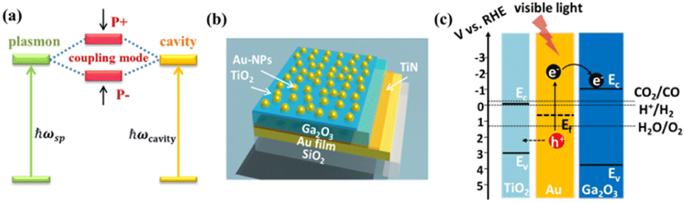 | ||
| Fig. 1 (a) Schematic diagram of energy splitting for strong coupling between the optical cavity and LSPR of Au-NPs. ωsp and ωcavity represent the angular frequency of LSPR and cavity resonance, respectively. (b) Schematic diagram of the TAGA structure. (c) Schematic of the LSPR-induced charge transfer in the TAGA structure. | ||
In this study, we fabricated a photoelectrode with modal strong coupling using Ga2O3 instead of TiO2, which improves the visible light absorption and photoelectric conversion efficiency of the Au-NPs/Ga2O3 photoelectrode. We studied its optical properties, photocurrent generation, and oxygen evolution using water as an electron source under visible light irradiation. Importantly, to obtain a β-Ga2O3 crystal phase that exhibits excellent photocatalytic properties, it was necessary to deposit a Ga2O3 layer at very high temperatures (higher than 500 °C).14 However, it was difficult to stably deposit Ga2O3 onto the Au film, which was the reflective mirror for the nanocavity under high-temperature conditions (500 °C or higher). To solve this problem, we developed a new method by depositing a thin layer of titanium nitride (TiN), a ceramic material that is stable at high temperatures above 1000 °C, with good electrical conductivity and relatively high reflectivity,15–17 on the Au film as a protection layer and used this TiN/Au-film as a reflective mirror. By depositing Ga2O3 on this reflective mirror, we succeeded in fabricating a Ga2O3/TiN/Au-film nanocavity at 600 °C. This method paves the way for the fabrication of photoelectrodes with modal strong coupling using various semiconductors that require relatively high deposition temperatures. We also confirmed that partial inlaying of Au-NPs in this modal strong coupling electrode [TiO2/Au-NPs/Ga2O3/TiN/Au-film (TAGA)], as indicated in Fig. 1b, plays an important role in improving the coupling strength and the charge separation of hot carriers. These results suggest that a photoelectrode with modal strong coupling using Ga2O3 would help reduce substances with a negative reduction potential higher than water by visible light irradiation using water as the electron source.
Materials and methods
TAGA photoanode preparation and characterization
As shown in Fig. S1,† a 100 nm Au film was deposited by helicon sputtering (ULVAC, MPS-4000C1/HC1) on silica glass (SiO2) with a size of 10 × 10 × 0.5 mm3, which was rinsed with acetone and methanol in an ultrasonic bath for 5 min each. Subsequently, an ultrathin TiN layer (5 nm) was deposited on the Au film using a multi-sputtering system with Ti and N2 as the target and reactive gas, respectively. The Sn-doped β-Ga2O3 target used in pulsed laser deposition (PAC-LMBE) was fabricated by sintering a powder mixture of SnO2 and β-Ga2O3 (Sn mole concentration of 0.5%) at 1400 °C for 10 hours. Sn-doped β-Ga2O3 films with different thicknesses were deposited on the TiN/Au-film/SiO2 substrate by controlling the pulse numbers at 600 °C with an oxygen pressure of 0.1 Pa. The laser energy and pulse frequency were set as 60 mJ and 5 Hz, respectively. A Ga2O3 film with a pulse number of 3000 was first deposited on TiN under a vacuum of 10−5 Pa without introducing oxygen, preventing the TiN thin film from oxidizing. Then, Au-NPs were loaded by annealing a 3 nm Au film deposited by electron-beam evaporation (EIKO Engineering, EB-580S) on a β-Ga2O3 film. The annealing temperature and duration were 400 °C and 2 hours, respectively. Finally, the Au-NPs on Ga2O3 were inlaid in a 4 nm TiO2 layer using a commercial hot-wall flow-type atomic layer deposition (ALD) reactor (SUNALETM R series, Picosun, Finland) at 300 °C.The phase structures of Sn-doped β-Ga2O3 powders and Ga2O3 films were investigated by X-ray diffraction (XRD, RIGAKU RINT-2000/PC) using Cu Kα radiation. Field-emission scanning electron microscopy (FE-SEM, JSM-6700FT, JEOL) with a maximum resolution of 1 nm was applied to identify the top-view morphology of TAGA. Optical reflectance and transmittance spectra were obtained using a photonic multichannel analyzer (PMA C7473, Hamamatsu Photonics) and spectroscopic reflectometer (Filmetrics, F20-UV).
Photoelectrochemical measurements
Before the photoelectrochemical (PEC) measurement, the backsides and sidewalls of the samples were coated with an In–Ga alloy with a weight ratio of 4![[thin space (1/6-em)]](https://www.rsc.org/images/entities/char_2009.gif) :1 to form an ohmic contact with the samples. Then, the samples were connected to a copper plate in a Teflon reaction cell that had a pinhole with a diameter of 2.0 mm on the lid. Subsequently, this cell was connected to an electrochemical analyzer (ALS/CH Instruments 852C, ALS) with a copper lead wire using a three-electrode system to measure the PEC performance. A platinum wire, a saturated calomel electrode (SCE), and 0.1 mol L−1 KOH aqueous solution were used as the counter electrode, reference electrode, and electrolyte. During the I–t measurement, a potential of +0.3 V vs. SCE was applied to the working photoanode under the illumination of the Xe lamp. We calculated the IPCE using the following formula:
:1 to form an ohmic contact with the samples. Then, the samples were connected to a copper plate in a Teflon reaction cell that had a pinhole with a diameter of 2.0 mm on the lid. Subsequently, this cell was connected to an electrochemical analyzer (ALS/CH Instruments 852C, ALS) with a copper lead wire using a three-electrode system to measure the PEC performance. A platinum wire, a saturated calomel electrode (SCE), and 0.1 mol L−1 KOH aqueous solution were used as the counter electrode, reference electrode, and electrolyte. During the I–t measurement, a potential of +0.3 V vs. SCE was applied to the working photoanode under the illumination of the Xe lamp. We calculated the IPCE using the following formula:where I is the photocurrent density, λ is the wavelength of incident light and Pin is the incident light intensity.
A two-electrode system was applied to carry out water splitting in our study, in which the TAGA samples and Pt wire were the working electrode and counter electrode, respectively. To estimate the O2 evolution amount from the oxidation of water determined by gas chromatography–mass spectrometry, 0.1 mol L−1 KOH aqueous prepared using the isotope and pure water (volume ratio H218O:H216O = 1:6) was used as the electrolyte. The Faraday efficiency was calculated according to the O2 and total charge amount.
Numerical simulations
The finite-difference time-domain (FDTD) method (FDTD Solutions, Lumerical) was applied to calculate the near-field distribution and intensity. A plane beam with linear polarization was used to illuminate the sample with a normal incidence. The investigated structure was simulated using perfectly matched layers along the z-direction and periodic boundary conditions along the x- and y-directions with a period of 20 nm. The Au-NPs were simulated by a model of ellipsoid spheres with diameters of 15 nm, 15 nm and 10 nm in the x, y and z directions, respectively. In the simulation, the refractive index of Au was taken from the data of Johnson and Christy.18 The mesh size was set as 0.02 nm. Ga2O3 and TiO2 were treated as dielectric materials with refractive indices of 1.9 and 2.4, respectively. In the near-field spectra simulation, the monitor was placed 1 nm above the interface of Au-NPs/Ga2O3. E and E0 indicate the electric field of the plasmonic field and incident light, respectively.Results and discussion
We first evaluated the role of the thin TiN layer between the Au film and Ga2O3. The crystalline structure of the Ga2O3 film deposited on the TiN/Au-film is shown in Fig. S2a (ESI),† which was assigned to β-Ga2O3.19 According to the top-view SEM image in Fig. S2b (ESI),† the Au-NPs were uniformly loaded on the surface of the Ga2O3 film with an average diameter of 15 nm and a standard deviation of 4.9 nm. Based on the electrochemical characterization shown in Fig. S3b (ESI),† the Au-NPs/Ga2O3/TiN/Au-film (AGA) sample shows good I–V properties. In contrast, the Au-NPs/Ga2O3/Au-film without a TiN layer shows undesirable I–V properties. Namely, the thin TiN layer improves the electrochemical properties of Ga2O3 deposited on the Au film. It is also noted that although the reflection of the Au-film decreases approximately 5% after depositing 5 nm-TiN, the TiN/Au-film still shows an adequate reflection, larger than 85% for wavelengths longer than 600 nm (see Fig. S3a (ESI)†), to be employed to construct an optical cavity.As illustrated in our previous work, hot electrons/holes generated through the nonradiative decay of LSPR could be separated by the Schottky barrier at the Au-NPs/Ga2O3 interface.12 Based on the positive effect of TiN on the electrochemical properties of Ga2O3, we assume the hot electrons injected into the CB of Ga2O3 take part in the reduction reaction based on the negative CB potential of Ga2O3. Conversely, hot holes were trapped by TiO2, improving the charge separation efficiency, as shown in Fig. 1c. Combined with the strong coupling effect, which has been demonstrated to improve the quantum efficiency of plasmon-induced chemical reactions,13 further improvements in the photoelectrochemical conversion efficiency are expected.
We deposited Ga2O3 films with different thicknesses on the TiN/Au-film substrate to form the cavity mode with tunable cavity resonance wavelengths. After the deposition of the Ga2O3 film on the TiN/Au-film, an obvious cavity mode was observed, as indicated in Fig. S4 (ESI)† by arrows. The cavity resonance (second order mode) wavelength shifted from 450 nm to 740 nm as the thickness of Ga2O3 increased from 135 nm to 293 nm. The TAGA absorption spectra calculated by −log(T + R) with various Ga2O3 thicknesses are presented in Fig. 2a, where T and R represent the transmittance and reflectance, respectively. Only one absorption band at approximately 470 nm appeared when the thickness of Ga2O3 was 135 nm because the cavity resonance wavelength was far away from the LSPR band of the Au-NPs located at approximately 635 nm, as shown in Fig. S5 (ESI).† When the thickness of Ga2O3 was larger than 150 nm, two absorption peaks gradually appeared because the cavity resonance wavelength shown in Fig. S4 (ESI)† shifted close to the LSPR wavelength. A tuning condition with two distinct absorption peaks was formed when the thickness of Ga2O3 was approximately 210 nm. While the thickness of the Ga2O3 films further increased, the dual bands gradually disappeared.
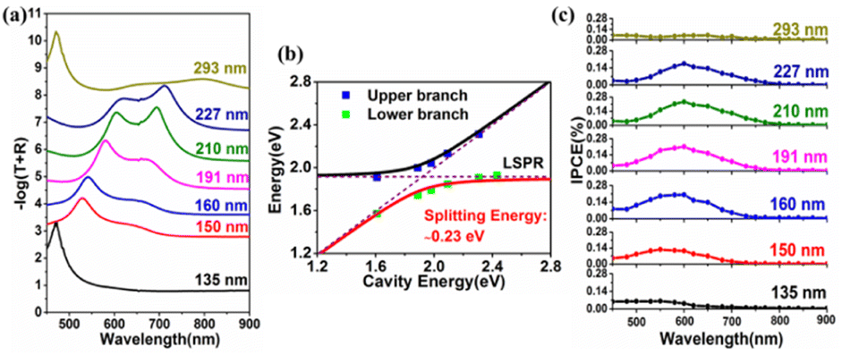 | ||
| Fig. 2 (a) Absorption spectra of TAGA with different thicknesses of Ga2O3 films. The thickness of the TiO2 layer partially inlaying Au-NPs was 4 nm. (b) Dispersion curve of the splitting absorption band for the TAGA structure. (c) IPCE spectra of TAGA measured in 0.1 mol L−1 KOH solution. The applied bias was +0.3 V vs. SCE. | ||
To further confirm whether this absorption band splitting resulted from the strong coupling, a dispersion curve of the TAGA structures plotting the absorption band energy as a function of the cavity resonance energy is shown in Fig. 2b. The black and red lines are the fittings using a coupled harmonic oscillator model.13 Lorentzian fitting was applied to calculate the peak energy of the separated dual bands for the TAGA structure represented by blue (upper branch) and green (lower branch) squares. The full width at half maximum of the upper and lower branches of the TAGA sample under tuning conditions separated by Lorentzian fitting was 0.23 eV and 0.17 eV, respectively, as shown in Fig. S6 (ESI).† According to the dispersion curve, the splitting energy of TAGA was calculated to be 0.23 eV, fulfilling the strong coupling criterion discussed in our previous study.20 It is noticeable that no coupling is formed in TiO2/Au-NPs/Ga2O3/sapphire (TAG) without an Au film, as shown in Fig. S5 (ESI).† As a result, the visible light absorption of the TAGA sample under strong coupling conditions was much higher than that of TAG.
Next, we measured the incident photon-to-current efficiency (IPCE) of the TAGA samples with different Ga2O3 thicknesses with a typical three-electrode electrochemical system in a 0.1 mol L−1 KOH aqueous solution, as shown in Fig. 2c. The IPCE showed obvious enhancement when the cavity wavelength was close to the LSPR wavelength. When the thickness was 210 nm, the IPCE reached a maximum value of 0.24% at 600 nm under tuning conditions. The I–t and I–V results of the TAGA samples under tuning conditions measured under darkness and 600 nm irradiation are shown in Fig. S7 (ESI).†
In this study, the role of the TiO2 layer used for partially inlaying the Au-NPs was also investigated. From the optical measurement in Fig. 3a, only one absorption band at approximately 630 nm was observed in the AGA structure with 210 nm Ga2O3, indicating that strong coupling was not formed. After inlaying Au-NPs in 4 nm TiO2 to construct TAGA, two absorption peaks appeared with an efficiently increased intensity, indicating that strong coupling between the plasmon mode and the cavity mode was formed, as discussed in Fig. 2. Because the LSPR mode of the Au-NPs was markedly enhanced after deposition in 4 nm TiO2, as shown in Fig. S8 (ESI),† the interaction between the plasmon mode and the cavity mode was strengthened, inducing a strong coupling condition. In addition, the TiO2 layer inlaying Au-NPs also led to a better spatial overlap between the cavity and LSPR mode, as illustrated in our previous study.13 From the photoelectrochemical measurements in Fig. 3b, the IPCE peak value of TAGA was 4.2 times larger than that of AGA without TiO2. According to the I–V curves in Fig. 3c, the onset potential of TAGA only showed a slight shift toward a positive potential compared with that of AGA. This means that TAGA has a significant reduction ability that is comparable to that of AGA, although the CB potential of TiO2 is more positive than that of Ga2O3. It has been reported that near-field enhancement strongly influences electron injection.21Fig. 3d shows the near-field distributions of TAGA and AGA simulated by the finite-difference time-domain (FDTD) method at a wavelength of 600 nm. The strong near-field enhancement marked by bright spots is located at the interface of Au-NPs/Ga2O3 for both TAGA and AGA. For TAGA, a higher-intensity near-field enhancement at the interface of Au-NPs/Ga2O3 was observed under a 600 nm wavelength under the coupling condition compared with the AGA structure. Furthermore, the integrated intensity of the near-field enhancement at the interface of Au-NPs/Ga2O3 was much higher than that of AGA without TiO2, as shown in Fig. 3e, resulting in a larger number of electron injections into the CB of Ga2O3.
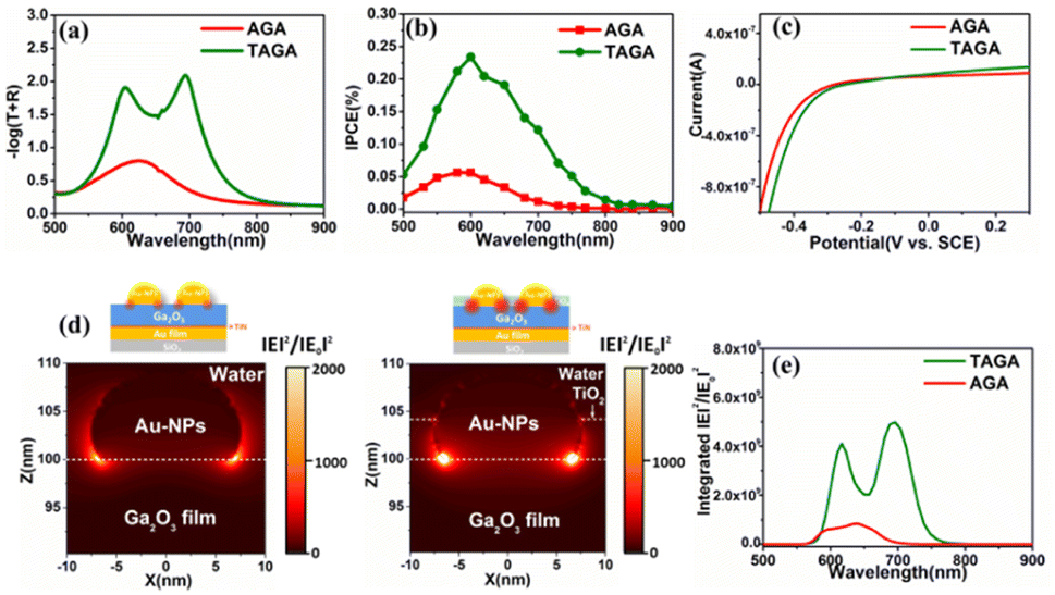 | ||
| Fig. 3 (a) Absorption spectra of TAGA and AGA. (b) IPCEs of TAGA and AGA measured in 0.1 mol L−1 KOH solution. The applied bias was +0.3 V vs. SCE. (c) I–V curves of TAGA and AGA measured in 0.1 mol L−1 KOH solution under dark conditions. (d) Near-field distribution at 600 nm irradiation of TAGA (right) and AGA (left) calculated by FDTD simulations. (e) Near-field spectra at the interface of Au-NPs/Ga2O3 of TAGA and AGA calculated by FDTD simulations. | ||
To further understand the role of the TiO2 layer and near-field enhancement in enhancing the IPCE, the TAG sample was also employed for comparison with the TAGA and AGA samples. TAGA under strong coupling conditions showed a 2.2-fold enhancement compared with TAG with a peak IPCE of 0.11% (see Fig. S9 (ESI)†). Therefore, the IPCE peak values are in the order of TAGA > TAG > AGA. Since the near-field enhancements at the interface of Au-NPs/Ga2O3 in TAG are smaller than those in AGA (see Fig. S10 (ESI)†), the larger IPCE in TAG compared with AGA should not result from the near-field enhancement. Alternatively, it could be attributed to the preferable hole-trapping ability of the TiO2 layer, which restrains electron/hole recombination and promotes plasmon-induced charge separation. Therefore, we might conclude that the hole-trapping ability of the TiO2 layer dominates the IPCE enhancement without strong coupling. Based on the efficient charge separation and significant near-field enhancement, the TAGA sample has superior performance in light absorption and photoelectrochemical conversion efficiency.
Water splitting using TAGA under visible light irradiation (λ > 450 nm) in a two-electrode system was detected by gas chromatography-mass spectrometry, as shown in Fig. 4. Although zero bias potential was applied between the Pt electrode and TAGA photoanode, O2 evolution from water oxidation was observed. The O2 evolution showed a linear relationship between the amount of O2 and the reaction time with an evolution rate of 23.9 nmol h−1 cm−2, as shown in Fig. 4a. The average Faraday efficiency of O2 evolution using TAGA under different reaction times remained stable at approximately 76%, as shown in Fig. 4b. No sacrificial electron donor or acceptor was used during the measurement. Additionally, there is no obvious change in surface morphology, particle size distribution, and TAGA absorption spectra before and after irradiation, and the generation of H2O2 was not found, as discussed in Fig. S11 (ESI).† These indicate that no side reaction or self-oxidation of the photoanode was observed. The relatively low Faraday efficiency of 76% probably results from the technical difficulty to collect all evolved O2. The photocurrent density of TAGA under visible irradiation tended to be quasi-stable after a few hours of irradiation (Fig. S12 (ESI)†). A linear increase in O2 evolution, as a function of irradiation time and the quasi-stable photocurrent, indicates the chemical stability of the photoanode. We also performed water splitting using TiO2/Au-NPs/Ga2O3/sapphire samples under the same measurement conditions as those used for TAGA. The O2 evolution over TiO2/Au-NPs/Ga2O3/sapphire showed a Faraday efficiency similar to that of the TAGA samples in Fig. 4b. However, the evolution rate (11.9 nmol h−1 cm−2) of TAG under the no-coupling condition was lower than half of that of TAGA. For photoelectrochemical reactions, external potentials have always been applied to further drive the related reductions in water splitting because of the insufficient CB potential of semiconductors.22 In this case, it is noticeable that the water splitting over TAGA was performed at zero bias potential. This could be explained by the negative CB potential of Ga2O3 positively affecting the reduction on the cathode, resulting in the improvement in the whole water splitting reaction.23 Based on the intrinsically negative CB potential, hot electrons injected into the CB of Ga2O3 and holes captured by TiO2 could take part in the redox reaction to generate H2 and O2 at zero bias potential.
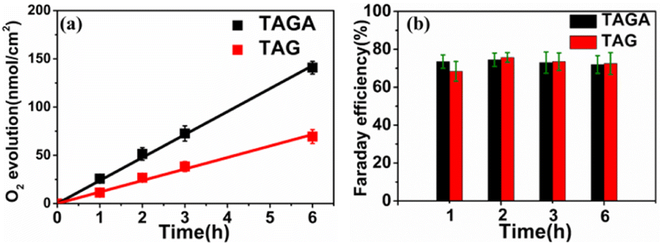 | ||
| Fig. 4 (a) O2 evolution and (b) Faraday efficiency using TAGA and TAG photoanodes illuminated by visible light (λ > 450 nm, 130 mW cm−2) under zero bias potential. The lines are the linear fittings. | ||
Conclusions
In summary, we developed a thin-film photoanode of TAGA with a negative CB potential to achieve zero-bias water splitting under visible light irradiation. A favorable I–V characteristic was obtained after adding a thin TiN film between Ga2O3 and the Au film, which acted as a protective layer for the Au film at high temperatures. Strong coupling was constructed when the cavity resonance wavelength of Ga2O3 on the TiN/Au-film matched the LSPR of the Au-NPs partially inlaid in the thin TiO2 layer. We successfully enhanced the visible light absorption and electron injection from the Au-NPs into Ga2O3 by applying strong coupling to the Ga2O3 system, which is intrinsically visible-light inactive. The photoelectric conversion efficiency under strong coupling also showed a noticeable enhancement compared to single-crystal Ga2O3. By taking advantage of the negative CB potential of Ga2O3, water splitting was successfully detected at zero bias potential. This result demonstrates that Ga2O3 exhibits significant prospects in relieving global environmental problems, especially CO2 reduction, based on its negative CB potential.Author contributions
Y. W. fabricated the samples, performed the measurements and analysed the data. X. S., T. O., and H. M. contributed to data analysis and discussion. H. M. supervised the work. Y. W. wrote the manuscript. All authors discussed the results and commented on the manuscript.Conflicts of interest
The authors declare no competing financial interest.Acknowledgements
We are grateful to Prof. V. Biju for his active involvement in the efforts to improve this manuscript. We acknowledge financial support from JSPS KAKENHI (Grant No. JP18H05205, JP18K05053, JP19H02737, JP19H04667, JP20H05083, JP22K19003, and JP22H05136), the Nanotechnology Platform (Hokkaido University), and the Dynamic Alliance for Open Innovation Bridging Human, Environment and Materials (Five-Star Alliance) of MEXT.Notes and references
- K. Maeda, J. Photochem. Photobiol., C, 2011, 12, 237–268 CrossRef CAS.
- J. Ran, M. Jaroniec and S. Z. Qiao, Adv. Mater., 2018, 30, 1704649 CrossRef.
- S. Chen, D. Liu and T. Peng, Sol. RRL, 2020, 5, 2000487 CrossRef.
- T. Takata, J. Jiang, Y. Sakata, M. Nakabayashi, N. Shibata, V. Nandal, K. Seki, T. Hisatomi and K. Domen, Nature, 2020, 581, 411–414 CrossRef CAS PubMed.
- Y. Yang, S. Niu, D. Han, T. Liu, G. Wang and Y. Li, Adv. Energy Mater., 2017, 7, 1700555 CrossRef.
- S. Choudhary, A. Solanki, S. Upadhyay, N. Singh, V. R. Satsangi, R. Shrivastav and S. Dass, J. Solid State Electrochem., 2013, 17, 2531–2538 CrossRef CAS.
- A. Corma and H. Garcia, J. Catal., 2013, 308, 168–175 CrossRef CAS.
- M. E. Aguirre, R. Zhou, A. J. Eugene, M. I. Guzman and M. A. Grela, Appl. Catal., B, 2017, 217, 485–493 CrossRef CAS.
- X. Wang, Q. Xu, M. Li, S. Shen, X. Wang, Y. Wang, Z. Feng, J. Shi, H. Han and C. Li, Angew. Chem., Int. Ed., 2012, 51, 13089–13092 CrossRef CAS PubMed.
- S. Kikkawa, K. Teramura, H. Asakura, S. Hosokawa and T. Tanaka, J. Phys. Chem. C, 2018, 122, 21132–21139 CrossRef CAS.
- T. Oshima, K. Kaminaga, H. Mashiko, A. Mukai, K. Sasaki, T. Masui, A. Kuramata, S. Yamakoshi and A. Ohtomo, Jpn. J. Appl. Phys., 2013, 52, 111102 CrossRef.
- Y. Wang, X. Shi, T. Oshikiri, S. Zu, K. Ueno and H. Misawa, Nanoscale, 2020, 12, 22674–22679 RSC.
- X. Shi, K. Ueno, T. Oshikiri, Q. Sun, K. Sasaki and H. Misawa, Nat. Nanotechnol., 2018, 13, 953–958 CrossRef CAS.
- K. Matsuzaki, H. Hiramatsu, K. Nomura, H. Yanagi, T. Kamiya, M. Hirano and H. Hosono, Thin Solid Films, 2006, 496, 37–41 CrossRef CAS.
- L. Hultman, Vacuum, 2000, 57, 1–30 CrossRef CAS.
- P. Patsalas, N. Kalfagiannis and S. Kassavetis, Materials, 2015, 8, 3128–3154 CrossRef CAS.
- D. Steinmüller-Nethl, R. Kovacs, E. Gornik and P. Rödhammer, Thin Solid Films, 1994, 237, 277–281 CrossRef.
- P. B. Johnson and R. W. Christy, Phys. Rev. B, 1972, 6, 4370–4379 CrossRef CAS.
- A. Goyal, B. S. Yadav, O. P. Thakur, A. K. Kapoor and R. Muralidharan, J. Alloys Compd., 2014, 583, 214–219 CrossRef CAS.
- T. Oshikiri, H. Jo, X. Shi and H. Misawa, Chem.–Eur. J., 2022, 28, e202200288 CrossRef CAS PubMed.
- Y. Suganami, T. Oshikiri, X. Shi and H. Misawa, Angew. Chem., Int. Ed., 2021, 60, 18438–18442 CrossRef CAS.
- S. Larson and Y. Zhao, Nanotechnology, 2016, 27, 255401 CrossRef PubMed.
- E. Fudo, A. Tanaka and H. Kominami, Catal. Sci. Technol., 2019, 9, 3047–3054 RSC.
Footnote |
| † Electronic supplementary information (ESI) available. See DOI: https://doi.org/10.1039/d2na00768a |
| This journal is © The Royal Society of Chemistry 2023 |