
 Open Access Article
 This Open Access Article is licensed under a
 Creative Commons Attribution 3.0 Unported Licence
Antiferromagnetic skyrmion-based high speed diode†
Namita
Bindal
 *,
Ravish Kumar
Raj
and
Brajesh Kumar
Kaushik
*,
Ravish Kumar
Raj
and
Brajesh Kumar
Kaushik
Department of Electronics and Communication Engineering, Indian Institute of Technology, Roorkee, Uttarakhand, India 247667. E-mail: namita@ec.iitr.ac.in; ravish_kr@ece.iitr.ac.in; bkk23fec@iitr.ac.in
First published on 15th December 2022
Abstract
Antiferromagnetic (AFM) skyrmions are favored over ferromagnetic (FM) skyrmions as they can be driven parallel to in-plane driving currents and eventually prevent the annihilation at the edges of nanotrack. In this study, an AFM skyrmion-based diode is proposed to realize the one-way skyrmion motion that is crucial for data processing in nanoelectronic and spintronic devices. The skyrmion transport is controlled by exploiting the staircase notch region in the middle of the nanotrack. By virtue of this, the micromagnetic interaction energy between the skyrmion and the notch edges generates a potential gradient that further gives rise to repulsive forces on the skyrmion. The resultant of the forces from the driving current and edge repulsions make the skyrmion move along the notch region to overcome the device window and reach the detection region. The notch is designed in such a way that it prevents the movement of the skyrmion in the reverse direction, thereby achieving diode functionality. The proposed device offers processing speed in the order of 103 m s−1, hence paving the way for the development of energy-efficient and high-speed devices in antiferromagnetic spintronics.
1 Introduction
Electrical diodes, operated under the effect of unidirectional current flux density, are the fundamental components of modern computation, communication, sensing, and artificial intelligence (AI) applications, enabling major advances in the fields of science and applied technology.1,2 Owing to the unidirectional operation of the electrical diode, considerable interest has been generated in various physical disciplines, including acoustics,3 microfluidics,4 photonics,5 thermodynamics,6 and micromagnetism.7 Magnetic skyrmions, a non-linear nanoscale spin texture, found in chiral magnets with broken inversion symmetry, can be viewed as viable information carriers due to their particle-like nature benefitting from unidirectional transport for diode applications.8,9 The unique properties of skyrmions, such as topological stability, nanoscale size, and ultra-low driving current density, make them ideal candidates for spintronic applications.10,11 Hence, skyrmions are predicted to bring in a new paradigm for spintronic devices.With an extensive study of the nucleation, dynamics, and detection of FM skyrmions, numerous devices such as racetrack memories,12,13 transistors,14 logic gates,15 oscillators,16 diodes,17 neurons,18 and synaptic devices19 have been designed. Moreover, ferromagnetic (FM) skyrmion experiences.
Magnus force and hence deviate from the driving current direction and may be annihilated at device edges.20 Hence, the skyrmion Hall effect (SkHE) poses a challenge for realistic applications that require a straight motion of a skyrmion along the direction of the applied current.21,22 However, antiferromagnetic (AFM) skyrmions follow a straight trajectory in the current direction, which is very promising for next-generation spintronic applications.23–25 AFM skyrmions have two sublattices, coupled by the inter-sublattice exchange interaction with no net magnetic moment, thereby vanishing the dipolar fields and completely eliminating the SkHE. AFM skyrmions are thus not only mathematically attractive but also offer major advantages that make them viable alternatives to FM skyrmions. Owing to the insensitivity of AFM skyrmions towards external magnetic fields, they are more robust against magnetic field perturbations, thus improving the stability and reliability of AFM skyrmion-based devices.26,27 The velocity of these skyrmions is around tens of order in magnitude greater than that of FM skyrmions.23 Furthermore, AFM materials are more abundant in nature, which include metals comprising Mn-based alloys, insulators, and semiconductors.28 These intriguing features of AFM skyrmions have encouraged the recent development of AFM spintronics, which has opened up a path to the notions of magnetic devices that could eventually replace conventional FM counterparts.
Recently, several FM skyrmion based diodes have been proposed.9,29–32 Various methods have been employed to control skyrmion transport, such as high anisotropy regions, asymmetric structures, modified edges and the SkHE effect. To confine FM skyrmions in the middle of the nanotrack, high-Ku regions at the top and bottom are also incorporated, thereby consuming much higher energy.29 Hence, in this work, an AFM skyrmion is used to design a diode that does not intrinsically exhibit SkHE, thereby enabling ultra-low power consumption and ultra-high processing speed of the device. In the proposed device, a notch region in the middle of the AFM nanotrack is incorporated. The notch region acts as a barrier, and allows the unidirectional motion of the skyrmion, thereby achieving P–N junction diode functionality. The competition between the forces, due to the driving current (by the application of a spin–orbit-torque (SOT)) and edge repulsions from the notch, guide the skyrmion through the device window to reach the detection region while preventing its motion in the reverse direction. The combined effects of driving current and the dimensions of notch steps on skyrmion dynamics have been investigated using micromagnetic simulations. Our findings could have a significant impact on fundamental physics and could be valuable in the development of AFM skyrmion-based energy-efficient devices for various applications including transistors, directional couplers, high-speed magnetic field sensors, and many telecommunication devices.
2 Methodology
Micromagnetic simulations were carried out using MuMax3 software33,34 to calculate the space and time-dependent magnetization evolution in nanoscale magnets based on the quantization of the sample, where the cell quantization is less than the exchange length. An AFM film with two sublattices of reversely aligned spins having magnetic moments![[m with combining right harpoon above (vector)]](https://www.rsc.org/images/entities/i_char_006d_20d1.gif) 1(
1(![[r with combining right harpoon above (vector)]](https://www.rsc.org/images/entities/i_char_0072_20d1.gif) ,t) and 2(,t), |1| = |2| = Ms/2 where Ms is the saturation magnetization was considered. The total magnetization was (,t) = 1(,t) + 2(,t) and the staggered magnetization was
,t) and 2(,t), |1| = |2| = Ms/2 where Ms is the saturation magnetization was considered. The total magnetization was (,t) = 1(,t) + 2(,t) and the staggered magnetization was ![[l with combining right harpoon above (vector)]](https://www.rsc.org/images/entities/i_char_006c_20d1.gif) (,t) = 1(,t) − 2(,t). The former was used to describe the canting of magnetic moments, and the latter was used to obtain the unit Néel vector that is related to AFM order.25
(,t) = 1(,t) − 2(,t). The former was used to describe the canting of magnetic moments, and the latter was used to obtain the unit Néel vector that is related to AFM order.25
The time-dependent magnetization dynamics were computed using the well-known Landau–Lifshitz–Gilbertz Slonczewski (LLGS) equation that is described as follows:35
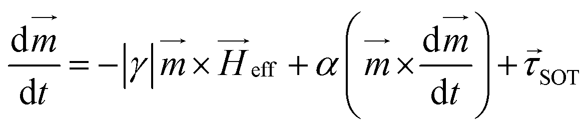 | (1) |
= (,t) = ![[M with combining right harpoon above (vector)]](https://www.rsc.org/images/entities/i_char_004d_20d1.gif) (,t)/Ms represents the normalized magnetization. α, γ, and Ms are the damping constant, gyromagnetic ratio, and saturation magnetization, respectively.
(,t)/Ms represents the normalized magnetization. α, γ, and Ms are the damping constant, gyromagnetic ratio, and saturation magnetization, respectively.
![[H with combining right harpoon above (vector)]](https://www.rsc.org/images/entities/i_char_0048_20d1.gif) eff = −δεAFM/μ0δ is the net field associated with various energies, such as magneto-crystalline anisotropy energy, exchange energy, and the Dzyaloshinskii–Moriya interaction (DMI) energy. The skyrmion is driven by the SOT mechanism that is given as follows:36
eff = −δεAFM/μ0δ is the net field associated with various energies, such as magneto-crystalline anisotropy energy, exchange energy, and the Dzyaloshinskii–Moriya interaction (DMI) energy. The skyrmion is driven by the SOT mechanism that is given as follows:36
![[small tau, Greek, vector]](https://www.rsc.org/images/entities/i_char_e1ca.gif) SOT = −γ × ( × H0 SOT = −γ × ( × H0![[a with combining right harpoon above (vector)]](https://www.rsc.org/images/entities/i_char_0061_20d1.gif) y) y) | (2) |
:35| εAFM = Jex[(∇mx)2 + (∇my)2 + (∇mz)2] − K0mz2 + D[mz(∇·) − (·∇)mz] | (3) |
This high mobility leads to a large spin diffusion length that reduces the deformation of the skyrmion in the presence of notches, thus enhancing the stability of a skyrmion in KMnF3 for long-term transportation.37,38 The material parameters used in the micromagnetic simulations were as follows:28,39 the nanotrack was considered to be 1024 × 300 × 1 nm3, cell size was 1 × 1 × 1 nm3. Ms,α, P, and Jex were 376 kA m−1, 0.005, 0.4, and −6.59 × 10⁻¹² J m−1, respectively. Magnetic anisotropy and interfacial DMI were considered as 1.22 × 10⁵ J m−3 and 1.2 × 10⁻³ J m−2, respectively.
3 Operation of the proposed device
Fig. 1(a) and (b) show schematics of the proposed AFM skyrmion-based diode for both forward and reverse bias, respectively. This device has three primary components, namely the nucleation point, four-step notch region, and a detection region. In the case of forward and reverse bias, the AFM Neel skyrmion is initially created at the nucleation point P0 = (x0, y0) = (100, 60) nm and (924, 60) nm, respectively with respect to the origin (O). A staircase is created in the middle of the nanotrack to display the impact of repulsive forces from the step edges, thereby facilitating the one-way motion of the skyrmion. The skyrmion is observed in the detection region once it overcomes the device window. The whole nanotrack has a fixed length and width as 1024 nm and 300 nm, respectively. A detection region has a length of 400 nm. Fig. 2 illustrates the attributes of the proposed device. Here, Sx and Sy represent the horizontal and vertical step lengths of the notch region, respectively. The device window is the control gate for the skyrmion during the forward/reverse motion. The 1st step vertical length is fixed as 70 nm irrespective of Sx and Sy. This is considered in such a way that when the skyrmion is moving in the forward direction, it should directly reach the first step corner so that the skyrmion immediately starts experiencing the force in the +y direction that facilitates its motion towards the detection region.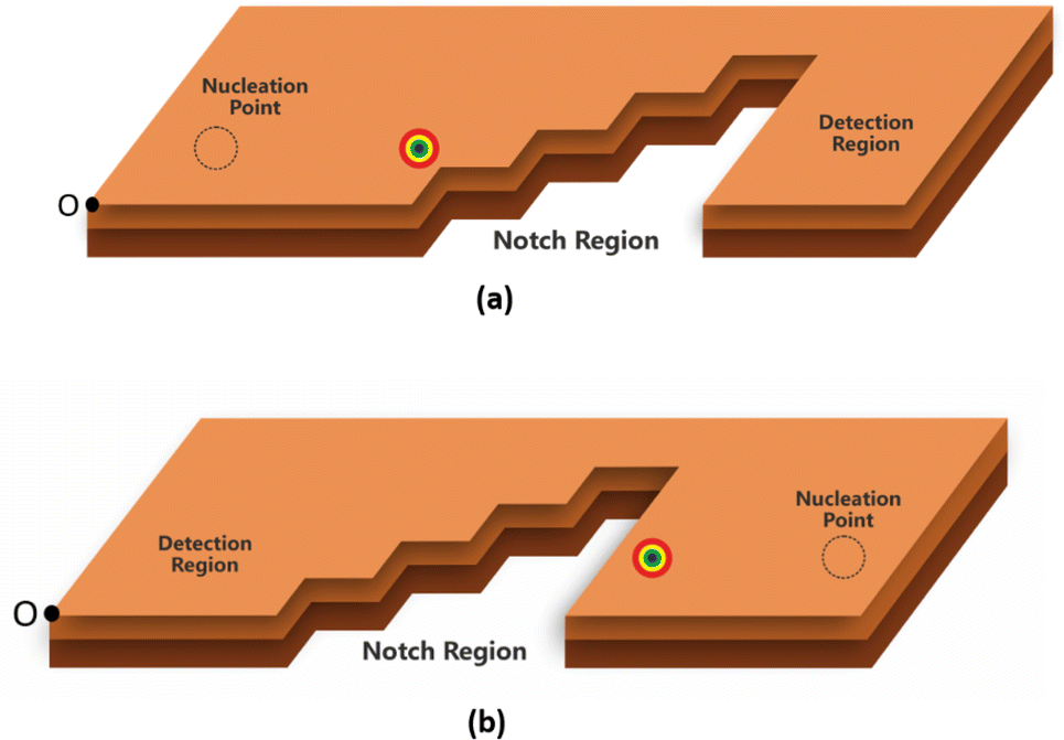 | ||
| Fig. 1 Schematic of the proposed device for (a) forward bias and (b) reverse bias. | ||
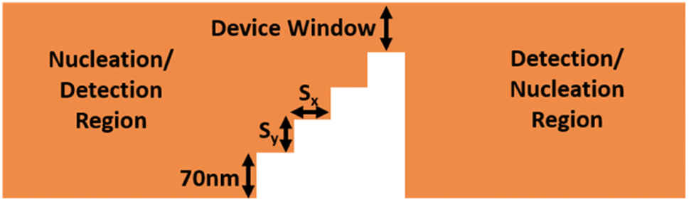 | ||
| Fig. 2 Attributes of the proposed device. | ||
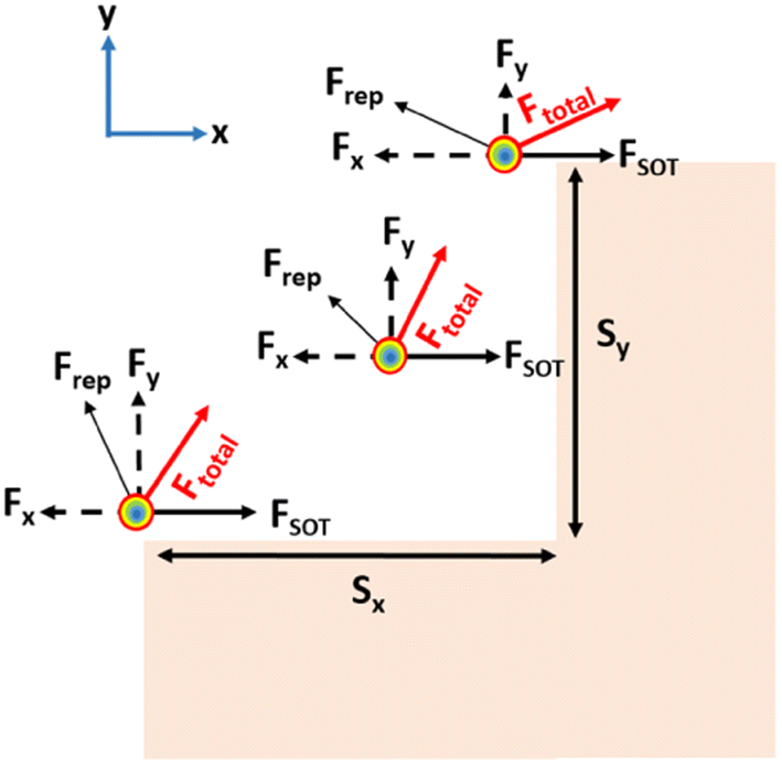
For the AFM skyrmion-based device to show diode functionality, it is mandatory to achieve a one-way motion of the skyrmion, apart from avoiding the deformation/annihilation of the skyrmion12 around the notch region. In the proposed device, a notch region facilitates the unidirectional motion of the skyrmion by bringing the significance of micromagnetic interaction energy that leads to repulsive forces on the skyrmion.40 In the case of forward motion, the skyrmion is nucleated at the left side (A1 point in Fig. 3) of the nanotrack, which is further drifted in the +x direction by the application of SOT. Once the skyrmion reaches near the notch region, the interaction between the core of the skyrmion and the notch edges enhance the potential energy. Hence, the spatial gradient  of the potential energy (U) gives rise to multiple repulsive forces (
 ) from the vertical step, and from the horizontal step and the geometric edge in both the x and y directions, respectively, which can be represented as:
 ![[F with combining right harpoon above (vector)]](https://www.rsc.org/images/entities/i_char_0046_20d1.gif) x = −∂U/∂xî and y = −∂U/∂yĵ. These forces along with the force due to driving current (total = rep + SOT) will lead to change in the position of the skyrmion position with respect to time, i.e. P(t) = (x(t), y(t)). An analysis of the skyrmion motion due to various forces acting in both the transverse and longitudinal directions determine the skyrmion's ability to overcome the device window and reach the detection region. When the skyrmion reaches the other side, it can be detected through the magnetic tunnel junction (MTJ) reader according to the tunnelling magnetoresistance effect.41 If the force due to the driving current is not sufficient, the skyrmion will be pinned near the device window. Alternatively, for high current densities, there is a probability of skyrmion deformation/annihilation. Hence, the analysis of the driving current and the horizontal and vertical step lengths (Sx and Sy) is required for proper device functionality, which is discussed in the next section.
x = −∂U/∂xî and y = −∂U/∂yĵ. These forces along with the force due to driving current (total = rep + SOT) will lead to change in the position of the skyrmion position with respect to time, i.e. P(t) = (x(t), y(t)). An analysis of the skyrmion motion due to various forces acting in both the transverse and longitudinal directions determine the skyrmion's ability to overcome the device window and reach the detection region. When the skyrmion reaches the other side, it can be detected through the magnetic tunnel junction (MTJ) reader according to the tunnelling magnetoresistance effect.41 If the force due to the driving current is not sufficient, the skyrmion will be pinned near the device window. Alternatively, for high current densities, there is a probability of skyrmion deformation/annihilation. Hence, the analysis of the driving current and the horizontal and vertical step lengths (Sx and Sy) is required for proper device functionality, which is discussed in the next section.
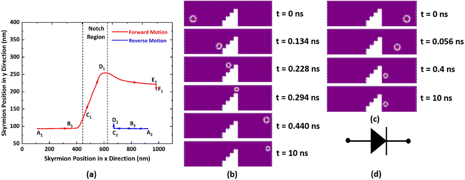 | ||
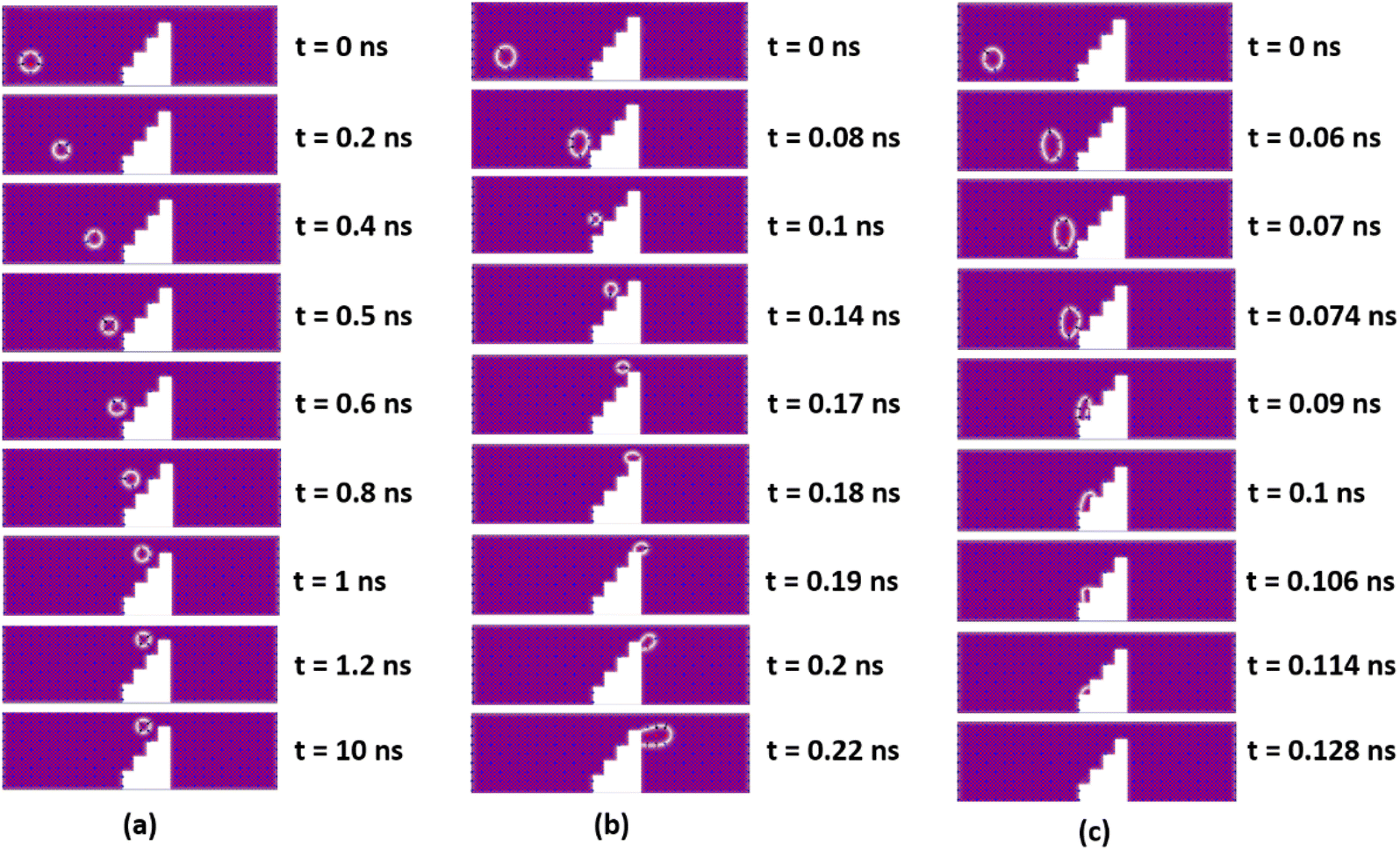
| Fig. 3 (a) Trajectories of the skyrmion for forward and reverse motion. (b and c) Snapshots of micromagnetic simulation at various positions for forward and reverse moving skyrmions, respectively. (Here, current density J, horizontal and vertical step lengths (i.e. Sx and Sy) are considered to be 20 GAm−2, 45 nm, 45 nm, respectively). (d) Diode symbol. | ||
In the case of reverse motion, the skyrmion is nucleated at the right side (A2 point in Fig. 3) of the nanotrack, which is driven in the −x direction using the driving current. The large vertical notch step (i.e. 205 nm as Sy = 45 nm) abruptly changes the potential energy, thereby acting as an energy barrier for the reverse-moving skyrmion. This generates a repulsive force in the direction opposite to the skyrmion motion. Hence, the skyrmion will not be able to overcome the device window, even for the case of high current densities, i.e. 40 GA m−2 (where 1 Giga Ampere (GA) = 109 A). Consequently, only one-way motion of the skyrmion can be realized when a staircase notch is created in the midst of the nanotrack. Snapshots of micromagnetic simulations for both forward and reverse bias are shown in Fig. 3(b) and (c), respectively, along with the conventional diode symbol (Fig. 3(d)).
4 Results and discussion
Working window of the proposed device
The horizontal and vertical step dimensions of the notch region, as well as the driving current, have a huge impact on the performance of the AFM skyrmion-based diode. Fig. 4 and 5 show the state diagrams with various horizontal and vertical step dimensions for forward and reverse moving skyrmions, respectively, under different driving current densities (5 GA m−2 ≤ J ≤ 40 GA m−2). It is worth noting that for higher current densities (J ≥ 37.5 GA m−2), the skyrmions are annihilated even at smaller step dimensions. Moreover, the lower the current density, the more likely it is for the forward-moving skyrmion to reach the detection region without any deformation/annihilation.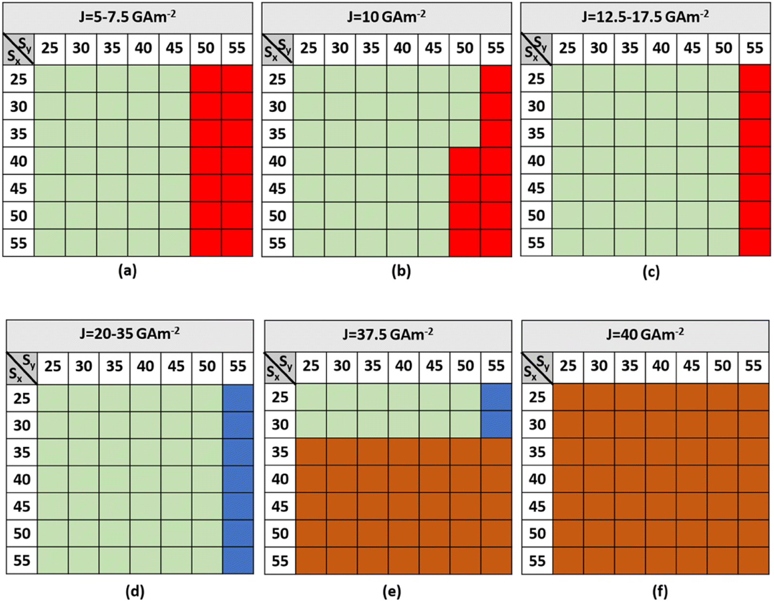 | ||
| Fig. 4 State diagrams for a forward-moving skyrmion with different horizontal and vertical step dimensions of the notch region for (a) 5 GA m−2 ≤ J ≤ 7.5 GA m−2 (b) J = 10 GA m−2 (c) 12.5 GA m−2 ≤ J ≤ 17.5 GA m−2 (d) 20 GA m−2 ≤ J ≤ 35 GA m−2 (e) J = 37.5 GA m−2 (f) J = 40 GA m−2. | ||
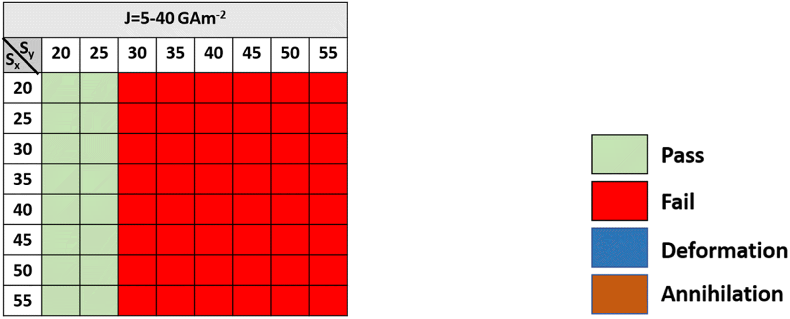 | ||
| Fig. 5 State diagram for a reverse-moving skyrmion with different horizontal and vertical step dimensions of the notch region for driving current densities in the range of 5–40 GA m−2. | ||
From Fig. 5, it can be observed that a reverse-moving skyrmion can bypass the device window if Sy < 30. But, when Sy > 30 then due to the large single vertical step (i.e. ≥160 nm) it is not possible for the reverse-moving skyrmion to overcome the device window. Hence, it can be stated that there should always be an abrupt change in the large single vertical step to prevent the reverse moving skyrmion reach the detection region. Hence, to facilitate one-way functionality of the skyrmion, the driving current density, horizontal and vertical step dimensions should be considered in the ranges of 5 GA m−2 ≤ J ≤ 35 GA m−2, 25 nm ≤ Sx ≤ 55 nm, and 30 nm ≤ Sy ≤ 45 nm, respectively. The following are the four dynamical behaviors of the forward-moving skyrmion that are observed for different combinations of step dimensions and driving current densities:
 | ||
| Fig. 6 Micromagnetic simulations illustrating (a) pinned, (b) deform (c) annihilate behaviors of a forward-moving skyrmion. | ||
Impact of current density and notch with Sx = Sy on the skyrmion dynamics
The velocity of the skyrmion on a nanotrack with respect to the skyrmion position is shown in Fig. 7(a) and (b). However, the variation in the skyrmion size with respect to its position is illustrated in Fig. 7(c). This is obtained for Sx = Sy = 45 nm under three different current densities i.e. J = 5GA m−2, J = 20 GA m−2, and J = 35 GA m−2. At first, the skyrmion follows a straight trajectory until it reaches the notch region. The x component of the velocity (vx) is directly proportional to the driving current density J.42 In this particular case, there is an approximately 300% increase in vx with a 300% increase in the current density whenever there is a negligible interaction between the skyrmion and the notch region. Moreover, the y component of the velocity (vy) before the notch region is zero due to the fact that an AFM skyrmion does not exhibit SkHE. Once the skyrmion reaches near the first step of the notch region, the skyrmion starts experiencing repulsion force from the vertical and horizontal steps, thereby deaccelerating in the −x direction against the driving force due to SOT and accelerating in the +y direction at that moment. Thereafter, the oscillatory behavior of the skyrmion is visible in both the velocity components vx and vy in the notch region. This is due to the fact that the distance between the core of the skyrmion and the vertical/horizontal step is varying continuously while the skyrmion is moving diagonally towards the device window. The maxima and minima of the oscillations are observed when the skyrmion is just before or after the step corner. This phenomenon is illustrated in Fig. 8. When the skyrmion reaches the device window, it will experience negligible repulsive force in the y direction. Hence, the driving current force accelerates the skyrmion in the +x direction. Once the skyrmion crosses the device window, it attains the uniform velocity vx but the force due to the geometric edge will act on the skyrmion in the −y direction, thereby moving the skyrmion in downward direction to some extent. After a few seconds, there will not be any movement of the skyrmion in the y direction due to an increase in the distance between the skyrmion and the geometric edge in the detection region. It is also observed that the processing speed of the proposed device is in the range of 600–4200 ms−1 for current densities of J = 5–35 GA m−2. A comparison of the numerical and analytical results of the AFM skyrmion velocity in the case of negligible impact of the repulsion force on the skyrmion from the notch edges is presented in the ESI Note 2.†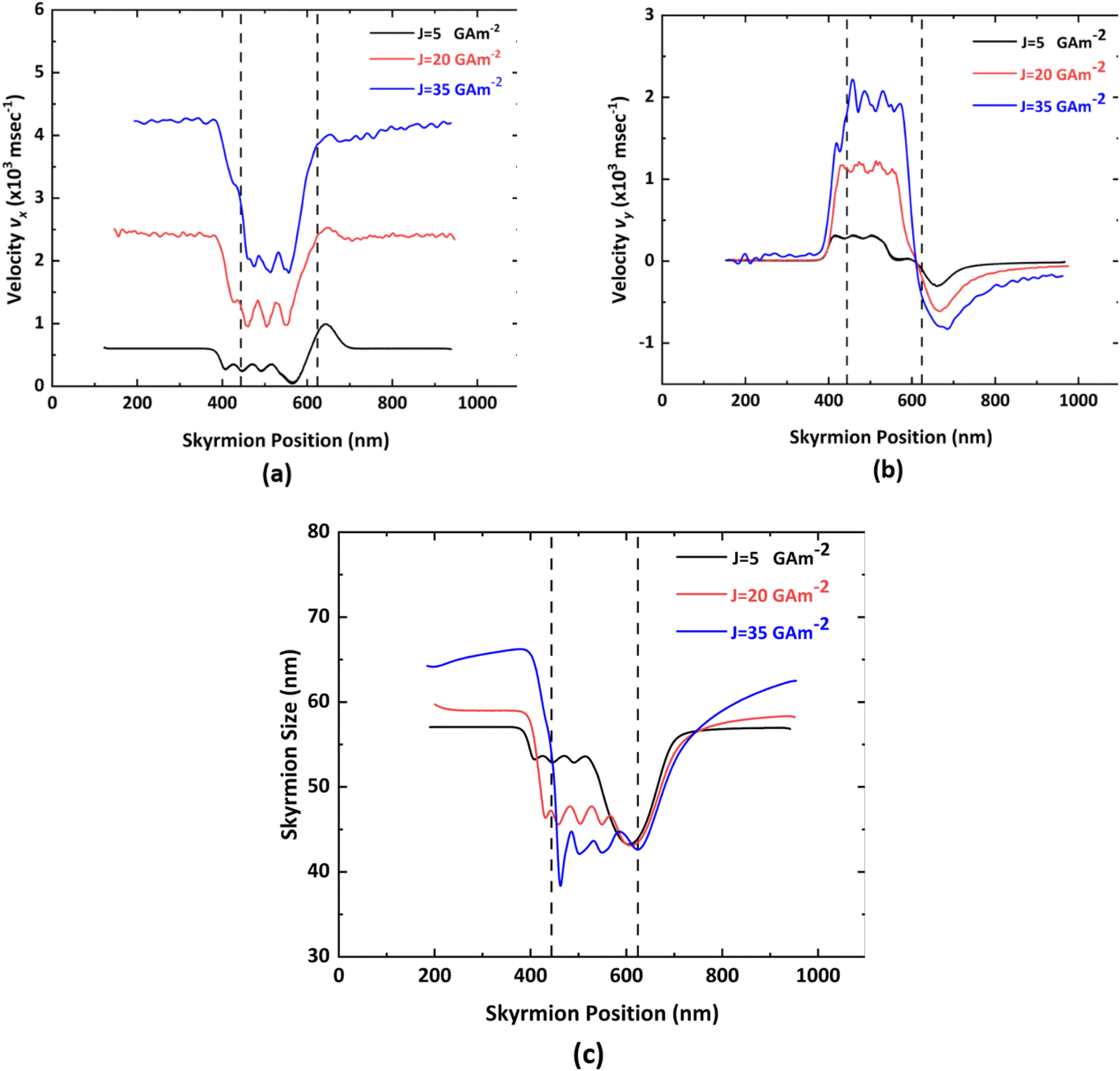 | ||
| Fig. 7 Variation of (a) velocity vx, (b) velocity vy, and (c) skyrmion size with respect to skyrmion position under different current densities for Sx = Sy = 45 nm in case of forward-moving skyrmion. Here, the notch region is between 444 nm and 624 nm represented by dotted lines. | ||
 | ||
| Fig. 8 The total force (Ftotal) acting on the skyrmion due to SOT (FSOT) and repulsion forces Fx and Fy from the vertical and horizontal steps, respectively, at different skyrmion positions. | ||
The skyrmion size is strongly affected by the total energy, which is the sum of the exchange energy, anisotropy energy, energy due to driving current, and interaction from the edges.43 For the proposed device, the change in the size of the skyrmion with respect to its position is shown in Fig. 7(c). For a specific current density, the size of the skyrmion will remain almost constant unless and until it reaches the notch region owing to the negligible interaction between the skyrmion and the notch edges. Once, the skyrmion reaches near the notch region, the size is reduced to some extent, and furthermore, it starts exhibiting oscillatory behavior while moving towards the device window by virtue of the different repulsion forces acting at the various steps. It can thus be concluded that the higher the repulsion force, the lower the skyrmion size.12 In the device window, the skyrmion size will be at a minimum as there will be an additional repulsion force at this moment. Once it overcomes the device window, it regains its initial size. Moreover, with an increase in the driving current density, the size of the AFM skyrmion is enlarged.44 Under large current densities, the skyrmion experiences very high repulsive force by virtue of increased potential energy gradient. Hence, the reduction in the skyrmion size is at a maximum. Alternatively, the amount of reduction in size is less for low current densities.
The variation in the normalized energy of a skyrmion with respect to the skyrmion position is shown in Fig. 9. During the forward motion of the skyrmion, the potential energy exhibits several sharp changes. These changes correspond to the different steps of the notch region, as when the skyrmion approaches the ends of all four steps of the notch region, oscillatory behavior is observed by virtue of the varying interaction between the skyrmion and the notch edge.
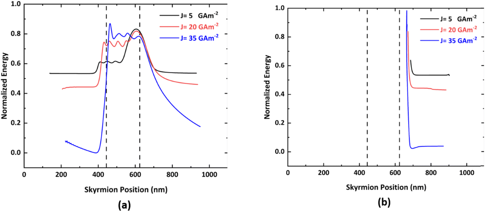 | ||
| Fig. 9 Variation of the total energy of the skyrmion with respect to skyrmion position under different current densities for Sx = Sy = 45 nm in the case of (a) forward-moving skyrmion and (b) reverse-moving skyrmion. | ||
With an increase in current, the distance between the skyrmion and the notch edges decreases significantly, thereby leading to an increase in the skyrmion boundary interaction potential.45 During the reverse motion of the skyrmion, there is a large single vertical step that will abruptly increase the potential energy gradient, thereby exerting a huge amount of repulsive force on the skyrmion and preventing two-way motion of the skyrmion. In addition, assuming the width and thickness of heavy metal (HM) to be 300 nm and 2 nm, respectively, and an input current density of 20 GA m−2, the average current flowing through the HM is IHM = 12 μA. The process time (tp) is 0.4 ns and the resistivity of the HM (ρHM) is assumed to be 1800 nΩ m.18 Consequently, the estimated total energy dissipation is 0.176 fJ. These advantages of the proposed device could further minimize the energy consumption of future AFM skyrmionic devices for information processing. Moreover, the comparison of the proposed device with other skyrmion based diodes is included in ESI Note 3.†
Impact of current density and asymmetric (Sx ≠ Sy) notch region on the skyrmion dynamics
While fabricating the proposed device, the step dimensions Sx and Sy might not be exactly equal, which makes the analysis of impact of the driving current density and notch with Sx ≠ Sy on skyrmion dynamics an important aspect. Fig. 10(a) and (b) show the variation in the velocity vx and skyrmion size with respect to the skyrmion position, respectively for different step ratios, i.e. Sx < Sy, Sx = Sy and Sx > Sy. When Sx < Sy, the repulsion from the vertical step in the −x direction dominates over the repulsion from the horizontal step in the +y direction, which reduces the velocity vx as well as the skyrmion size to the highest extent near the notch region. Moreover, if Sx > Sy, then the repulsion in the +y direction dominates over repulsion in the −x direction. Hence, for Sx > Sy, the velocity vx and the skyrmion size are much higher compared to that for Sx < Sy.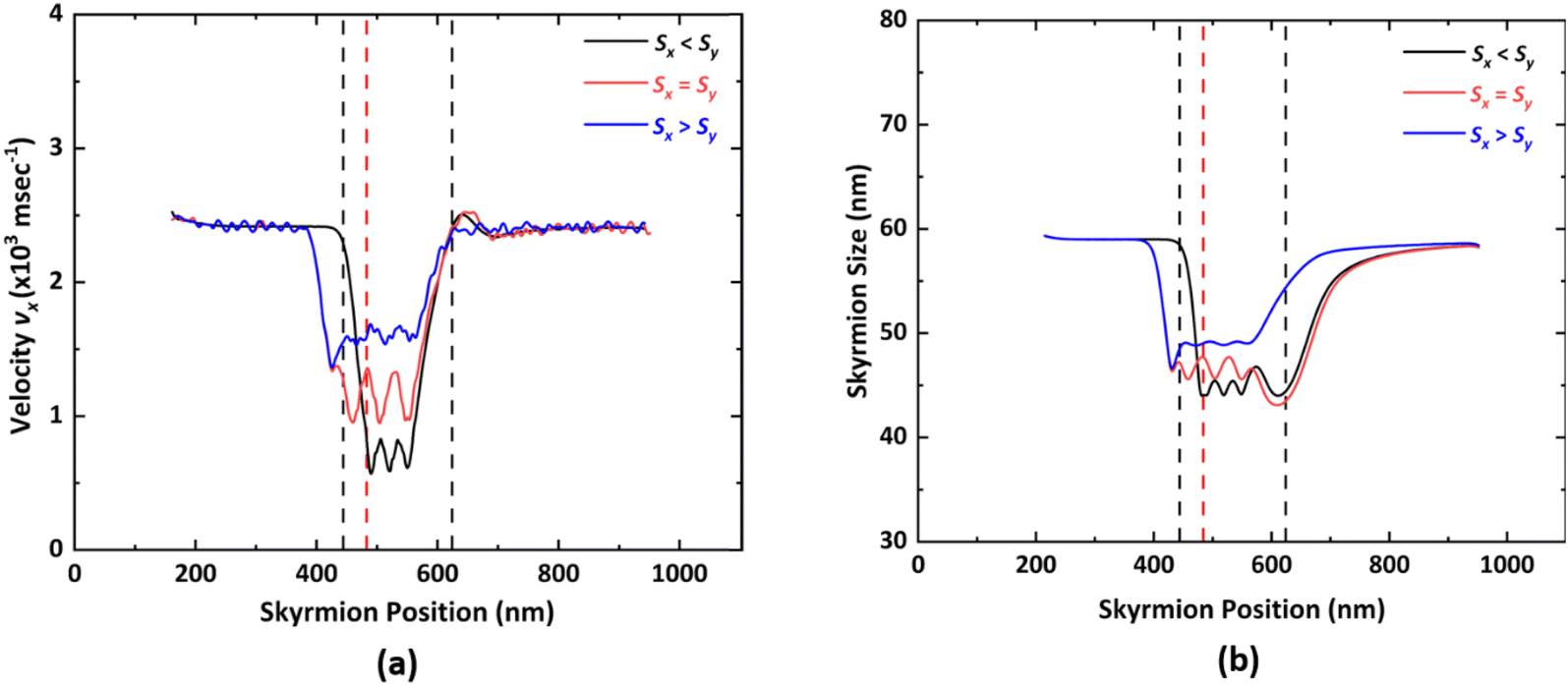 | ||
| Fig. 10 Variation of (a) velocity vx and (b) skyrmion size with respect to skyrmion position under different step ratios for current density J = 20 GA m−2 in case of forward-moving skyrmion. For Sx = Sy and Sx > Sy, notch region is between 444 nm to 624 nm. For Sx < Sy, notch region is between 484 nm and 624 nm, represented by dotted lines. | ||
Conclusion
An AFM skyrmion-based diode was designed using a staircase notch region at the middle of the nanotrack, which makes the proposed device highly energy efficient. The notch region was exploited to induce a change in potential energy during the skyrmion motion, which led to various repulsive forces acting on it. The physical realization of a notch in any device is a challenging task. However, it is possible to achieve the precise notch dimensions using high-quality fabrication techniques.46–48 In this work, the skyrmion motion under different driving current densities and horizontal and vertical step dimensions has been demonstrated to identify the proper working window of the proposed device. The research results show that to achieve one-way motion of the skyrmion, i.e. motion under different driving current densities and horizontal and vertical step dimensions has been demonstrated to identify the diode functionality, the device must be operated under in the range of 5 GA m−2 ≤ J ≤ 35 GA m−2, 25 nm ≤ Sx ≤ 55 nm, and 30 nm ≤ Sy ≤ 45 nm. The forward-moving skyrmion will bypass the device window, while the reverse-moving skyrmion gets stuck near the large single vertical step. Here, we not only analyzed the energy variation of the skyrmion during its motion but also identified the variation in the velocity and skyrmion size during the skyrmion motion on the nanotrack under different driving current densities and geometric parameters of the notch region. This device offers very low energy consumption and high processing speed, making it a potential candidate for the implementation of future AFM skyrmionic devices for information processing.Conflicts of interest
There are no conflicts to declare.Acknowledgements
The authors would like to acknowledge the Ministry of Education, Government of India, Council of Scientific and Industrial Research (CSIR) Grant No. 09/0143(11108)/2021-EMR-, and Science and Engineering Research Board (SERB), Department of Science and Technology, Government of India under Grant CRG/2019/004551 for providing the funding to carry out the research work.References
- J. Lee, N. Hong, W. Hong, D. Kim, Y. Hwang, J. Jang and H. Kang, Adv. Mater. Technol., 2021, 2100923 Search PubMed , 1–10..
- S. Zhao, F. Blaabjerg and H. Wang, IEEE Transactions on Power Electronics, 2020, 36, 4633–4658 Search PubMed.
- A. E. X.-F. Li, X. Ni, L. Feng, M. H. Lu, C. He and Y.-F. Chen, Phys. Rev. Lett., 2011, 106, 084301 CrossRef PubMed , 1–4..
- X. Huo and G. Yossifon, Phys. Rev. Lett., 2019, 123, 194502 CrossRef CAS PubMed , 1–6..
- D. W. Wang, H. T. Zhou, M. J. Guo, J. X. Zhang, J. Evers and S. Y. Zhu, Phys. Rev. Lett., 2013, 110, 093901 CrossRef PubMed , 1–5..
- C. W. Chang, D. Okawa, A. Majumdar and A. Zettl, Science, 2006, 314, 5802 Search PubMed , 112–1124..
- J. Wang, et al. , Appl. Phys. Lett., 2020, 117, 202401 CrossRef CAS.
- A. Fert, N. Reyren and V. Cros, Nat. Rev. Mater., 2017, 2, 17031 CrossRef CAS , 1–15..
- D. H. Jung, H. S. Han, N. Kim, G. Kim, S. Jeong, S. Lee, M. Kang, M. Y. Im and K. S. Lee, Phys. Rev. B: Condens. Matter Mater. Phys., 2021, 104, L060408 CrossRef CAS , 1–6..
- J. Iwasaki, W. Koshibae and N. Nagaosa, Nano Lett., 2014, 14(8), 4432–4437 CrossRef CAS PubMed.
- S. Woo, K. M. Song, H. S. Han, M. S. Jung, M. Y. Im, K. S. Lee, K. S. Song, P. Fischer, J. I. Hong, J. W. Choi, B. C. Min, H. C. Koo and J. Chang, Nat. Commun., 2017, 8, 15573 CrossRef CAS PubMed , 1–8..
- X. Zhang, G. Zhao, H. Fangohr, J. P. Liu, W. X. Xia, J. Xia and F. J. Morvan, Sci. Rep., 2015, 5, 7643 CrossRef CAS PubMed , 1–6..
- S. Honda, T. Yae and T. Ohsawa, IEEE Trans. Magn., 2019, 55, 1–4 Search PubMed.
- I. S. Hong and K. J. Lee, Appl. Phys. Lett., 2019, 115, 072406 CrossRef.
- S. Luo, M. Song, X. Li, Y. Zhang, J. Hong, X. Yang, X. Zou, N. Xu and L. You, Nano Lett., 2018, 18, 1180–1184 CrossRef CAS PubMed.
- L. Shen, et al. , Appl. Phys. Lett., 2019, 114, 042402 CrossRef.
- L. Song, et al. , J. Magn. Magn. Mater., 2021, 532, 167975 CrossRef CAS.
- S. Li, W. Kang, Y. Huang, X. Zhang, Y. Zhou and W. Zhao, Nanotechnology, 2017, 28, 31LT01 CrossRef PubMed.
- K. M. Song, J. S. Jeong and B. Pan, et al. , Nat. Electron., 2020, 3, 148–155 CrossRef.
- G. Chen, Nat. Phys., 2017, 13, 112–113 Search PubMed.
- X. Zhang, Y. Zhou and M. Ezawa, Nat. Commun., 2016, 7, 10293 Search PubMed.
- L. Shen, et al. , Phys. Rev. Lett., 2020, 124, 037202 CrossRef CAS PubMed.
- X. Zhang, Y. Zhou and M. Ezawa, Sci. Rep., 2016, 6, 24795 CrossRef CAS PubMed.
- N. Bindal, C. A. C. Ian, W. S. Lew and B. K. Kaushik, Nanotechnology, 2021, 32, 21 CrossRef PubMed.
- L. Shen, et al. , Phys. Rev. B, 2018, 98, 13448 Search PubMed.
- N. Bindal, R. K. Raj and B. K. Kaushik, J. Phys. D: Appl. Phys., 2022, 55, 34 CrossRef.
- G. Yu, A. Jenkins and X. Ma, et al. , Nano Lett., 2018, 18, 2 Search PubMed.
- J. Barker and O. A. Tretiakov, Phys. Rev. Lett., 2016, 116, 147203 CrossRef PubMed.
- L. Zhao, X. Liang, J. Xia, G. Zhao and Y. Zhou, Nanoscale, 2020, 12, 9507 RSC.
- J. Wang, et al. , Appl. Phys. Lett., 2020, 117, 202401 CrossRef CAS.
- Y. Shu, et al. , Appl. Phys. Lett., 2022, 121, 042402 CrossRef CAS.
- Y. Feng, et al. , IEEE Trans. Electron Devices, 2022, 69, 3 Search PubMed.
- A. Vansteenkiste, J. Leliaert, M. Dvornik, M. Helsen, F. G. Sanchez and B. V. Waeyenberge, AIP Adv., 2014, 4, 107133 CrossRef.
- J. Leliaert, M. Dvornik, J. Mulkers, J. D. Clercq, M. V. Milošević and B. V. Waeyenberge, J. Phys. D: Appl. Phys., 2018, 51, 123002 CrossRef.
- X. Liang, J. Xia, X. Zhang, M. Ezawa, O. A. Tretiakov, X. Liu, L. Qiu, G. Zhao and Y. Zhou, Appl. Phys. Lett., 2021, 119, 062403 CrossRef CAS.
- E. Martinez, S. Emori and G. S. D Beach, Appl. Phys. Lett., 2013, 103, 072406 CrossRef.
- R. T. Wang, E. G. Tai, J. Y. Chen, G. Xu, R. LaPierre, N. I. Goktas and N. Hu, Ceram. Int., 2019, 45, 1 CrossRef.
- S. Wang, et al. , Nat. Electron., 2019, 98–107 CrossRef.
- P. E. Roy, J. Appl. Phys., 2021, 129, 193902 CrossRef CAS.
- A. F. Schäffer, L. Rózsa, J. Berakdar, E. Y. Vedmedenko and R. Wiesendanger, Commununications Physics, 2019, 2, 72 Search PubMed.
- N. Djavid and R. K. Lake, Phys. Rev. B, 2020, 102, 024419 CrossRef CAS.
- K. Litzius, J. Leliaert and P. Bassirian, et al. , Nat. Electron., 2020, 3, 30–36 CrossRef CAS.
- X. S. Wang, X. H. Y. Yuan and X. R. Wang, Communication Physics, 2018, 1, 31 CrossRef.
- Z. Huang, Z. Jin, X. Zhang and Z. P. Hou, Phys. Status Solidi RRL, 2020, 14, 8 Search PubMed.
- R. Brearton, G. V. Laan and T. Hesjedal, Phys. Rev. B: Condens. Matter Mater. Phys., 2020, 101, 134422 CrossRef CAS.
- Y. Gao, B. You, J. Wang, Y. Yuan, L. J. Wei, H. Q. Tu, W. Zhang and J. Du, Appl. Phys. Lett., 2018, 8, 055924 Search PubMed.
- J. J. W Goertz, G. Ziemys, I. Eichwald, M. Becherer, H. J. M. Swagten and S. B. Gamm, AIP Adv., 2016, 6, 056407 CrossRef.
- Y. Gao, et al. , Sci. Rep., 2016, 6, 32617 CrossRef CAS PubMed.
Footnote |
| † Electronic supplementary information (ESI) available. See DOI: https://doi.org/10.1039/d2na00748g |
| This journal is © The Royal Society of Chemistry 2023 |