
 Open Access Article
 This Open Access Article is licensed under a
 Creative Commons Attribution 3.0 Unported Licence
Formation of a vertical SnSe/SnSe2 p–n heterojunction by NH3 plasma-induced phase transformation
Yi
Li
 *ab,
Juanmei
Duan
ab,
Yonder
Berencén
a,
René
Hübner
a,
Hsu-Sheng
Tsai
a,
Chia-Nung
Kuo
cd,
Chin Shan
Lue
cd,
Manfred
Helm
ab,
Shengqiang
Zhou
a and
Slawomir
Prucnal
*a
*ab,
Juanmei
Duan
ab,
Yonder
Berencén
a,
René
Hübner
a,
Hsu-Sheng
Tsai
a,
Chia-Nung
Kuo
cd,
Chin Shan
Lue
cd,
Manfred
Helm
ab,
Shengqiang
Zhou
a and
Slawomir
Prucnal
*a
aHelmholtz-Zentrum Dresden-Rossendorf, Institute of Ion Beam Physics and Materials Research, Bautzner Landstrasse 400, D-01328 Dresden, Germany. E-mail: y.li@hzdr.de; s.prucnal@hzdr.de
bTechnische Universität Dresden, D-01062 Dresden, Germany
cDepartment of Physics, National Cheng Kung University, Tainan 70101, Taiwan
dTaiwan Consortium of Emergent Crystalline Materials, Ministry of Science and Technology, Taipei 10601, Taiwan
First published on 25th November 2022
Abstract
Layered van der Waals crystals exhibit unique properties making them attractive for applications in nanoelectronics, optoelectronics, and sensing. The integration of two-dimensional materials with complementary metal-oxide-semiconductor (CMOS) technology requires controllable n- and p-type doping. In this work, we demonstrate the fabrication of vertical p–n heterojunctions made of p-type tin monoselenide (SnSe) and n-type tin diselenide (SnSe2). The p–n heterojunction is created in a single flake by the NH3-plasma-assisted phase transformation from SnSe2 to SnSe. We show that the transformation rate and crystal quality strongly depend on plasma parameters like plasma power, temperature, partial pressure, NH3 flow, and duration of plasma treatment. With optimal plasma parameters, the full transformation of SnSe2 flakes into SnSe is achieved within a few seconds. The crystal quality and the topography of the fabricated SnSe–SnSe2 heterostructures are investigated using micro-Raman spectroscopy and cross-sectional transmission electron microscopy. The formation of a p–n junction is verified by current–voltage measurements.
Introduction
Graphene is the most investigated 2D material, but due to the lack of a bandgap, the potential application of graphene is rather limited. Nevertheless, the discovery of ultra-high carrier mobility in atomically thin graphene layers and outstanding optical properties1 stimulated scientists to explore other materials, namely layered van der Waals crystals.2–7 In contrast to graphene, most of them have an optical bandgap in the energy range from about 6 eV for h-BN down to tens of meV for different transition metal dichalcogenides (TMDs) or graphene ribbons.8 The as-synthetized mono- and dichalcogenides have well-defined native conductivity, which can be changed by external doping or by defect engineering. Moreover, the mono- or a few-layer-thick 2D mono- and dichalcogenides possess a direct bandgap with an emission in the visible and mid-infrared spectral range, making them attractive for optoelectronics.SnSe is a p-type semiconductor with an orthorhombic crystal structure.9 The indirect and direct bandgaps of SnSe are 0.9 and 1.2 eV, respectively. SnSe is thermally stable with a melting point as high as 880 °C and can be kept in an ambient environment for a few weeks without detectable degradation. It can be fabricated by selenization of Sn thin films at about 550–570 °C.10 Fernandes et al. showed that selenization of Sn thin films in the temperature range of about 300 to 470 °C leads to the formation of SnSe2 with a trigonal CdI2-type crystal structure of C6 space symmetry.11 The as-synthetized SnSe2 is contaminated with Se atoms at the surface which can be later removed by annealing in a vacuum. In contrast to monoselenide, SnSe2 is an n-type semiconductor with an indirect bandgap of about 0.95 eV, and the allowed direct optical transition is at about 2.5 eV, while the band gap of bulk SnS2 is 2.18 eV and that of monolayer SnS2 is 2.41 eV, respectively. It was shown that both SnSe and SnSe2 are attractive for photovoltaics due to their efficient light harvesting ability, and they show outstanding thermoelectric properties with a figure of merit ZT factor as high as 2.2.12 Combining SnSe2 with SnSe allows the fabrication of vertical p–n junctions. Besides selenization of Sn, mono- and dichalcogenides can be synthetized using a wide variety of fabrication techniques, like solvothermal and chemical bath deposition,13–15 electrodeposition, spray pyrolysis,16,17 chemical vapor deposition or pulsed laser deposition.11 To this day, the fabrication of either lateral or vertical heterostructures on the same substrate is challenging due to the different growth conditions for different materials. The phenomenon of phase transformation observed on some of the chalcogenides is a very promising method to fabricate vertical p–n junctions. The phase transformation in SnSe2 and SnSe bulk crystals was reported by Albers and Verberkt for the first time.18 Single-crystalline SnSe and SnSe2 can be grown by saturation of the Sn–Se melt with Se or Sn, respectively. SnSe2–SnSe mixed crystals were obtained by changing the solidification speed. Sutter et al. showed that using high-energy electrons, both SnSe2 and SnS2 can be converted into monoselenide and monosulfide, respectively.19 According to DFT calculations, the electron energy required to promote the phase transformation of dichalcogenides into monochalcogenides must be in the range of 80 keV or higher.19 Due to the deep penetration depth of highly energetic electrons into Sn-dichalcogenides, monochalcogenides are created simultaneously at different depths and finally, the whole flake/layer is converted into the corresponding monochalcogenide. Zhou et al. used high-temperature annealing of SnS2 flakes in an Ar atmosphere for phase transformation.20 In particular, they showed that after annealing at 600 °C in a continuous Ar flow, SnS2 flakes were converted into monosulfides due to the sublimation of S atoms from the surface. A similar effect was obtained by annealing Sn-dichalcogenides in a vacuum. The full conversion of the dichalcogenides into monochalcogenides occurred after annealing at about 500 °C for 90 min.21 More precise control of the transformation of dichalcogenides into monochalcogenides is achieved by applying an Ar plasma. Recently, Kim et al. used an Ar plasma to remove S atoms from the surface of SnS2 films, and the formation of p–n vertical junctions between SnS and SnS2 was demonstrated.22
In this work, we present the fabrication of vertical p–n heterojunctions using NH3-plasma-assisted phase transformation of n-type trigonal dichalcogenides (SnSe2) into p-type orthorhombic monochalcogenides (SnSe). Cross-sectional transmission electron microscopy (TEM) images reveal an atomically flat interface between SnSe2 and SnSe. We also show that the phase change and crystal quality of the transformed flakes strongly depend on plasma power, time, partial pressures, and temperature. The formation of the p–n heterojunction is confirmed by the rectifying behavior of the current–voltage characteristics and the change of the phonon spectra. After NH3 plasma treatment, the investigated flakes exhibit four new Raman peaks which are identified as the Ag1 (70 cm−1), B3g (100 cm−1), Ag2 (120 cm−1), and Ag3 (147 cm−1) Raman-active phonon modes in SnSe.23
Experimental part
SnSe and SnSe2 bulk crystals were synthetized by the Bridgman method. For the SnSe crystal, a stoichiometric ratio between Sn and Se (99.999% purity for each element) was used. Sn and Se were loaded into a small quartz tube and sealed into a second ampoule to avoid cracking upon cooling. The charged ampoule was heated in a vertical furnace to 910 °C for 12 h and kept at 910 °C for 24–48 h for homogenization. After that, the ampoule was slowly cooled to 750 °C at a rate of 1 °C h−1 and kept at this temperature for 50 h. A similar process was used to fabricate SnSe2. Due to the lower melting point, the dwell temperature was reduced to 700 °C. After the successful fabrication of bulk crystals, micro-flakes with layer thicknesses from a mono-layer to tens of nanometers were obtained by conventional mechanical exfoliation using Nitto tape SPV 224PR-MJ. SnSe and SnSe2 flakes were transferred onto a Si wafer covered with 75 nm of SiNx. The SiNx layer was deposited on the Si wafer using plasma-enhanced chemical vapor deposition (PECVD) at 350 °C. The SiNx films show better optical contrast for thin 2D materials than the conventionally used 290 nm thick SiO2.24 To improve the adhesion between the flakes and the substrates, the samples with the tape (just before transfer) were heated up to 70 °C for 4 min and the tape was taken out. We inspected the influence of different N2 and NH3 plasma powers, times, temperatures, and partial pressures on the phase-change phenomenon in SnSe2. For the sake of comparison, the SnSe flakes were processed under the same conditions. Shortly after exfoliation, the samples with SnSe2 were placed in a PECVD load-lock chamber. Our PECVD system allows for both the deposition of a SiNx capping layer and the N2/NH3 plasma treatment. Reference SnSe and SnSe2 samples were covered with a 6 nm-thick SiNx film deposited by PECVD at 200 °C, the temperature at which no phase change was detected. The growth rate of SiN is about 10 nm min−1. The SiNx layer is used to protect the 2D materials from contamination. The N2 or NH3 plasma treatment was performed prior to SiNx capping layer deposition without breaking the vacuum. The NH3 plasma parameters are summarized in Table 1. The same parameters were used for N2 plasma treatment, but no phase transformation was detected. Here, we present the data obtained for a plasma power of 20 W.| Temperature (°C) | Time (s) | Pressure (mTorr) | Plasma power (W) | SnSe2 phase | SnSe phase | Phase Mixture |
|---|---|---|---|---|---|---|
| 200 | <60 | 500–800 | 20 | √ | — | — |
| 250 | 5–30 | 500–800 | 20 | √ | ||
| 300 | 5–30 | 500–800 | 20 | √ | ||
| 350 | 5–30 | 500–800 | 20 | √ | ||
| 400 | 5–30 | 500–800 | 20 | √ |
Increasing the plasma power considerably above 20 W makes it difficult to control the phase transformation, while lower power reduces the concentration of H ions in the plasma, making the process less efficient. If the pressure drops significantly below 500 mTorr, the plasma treatment time must increase clearly beyond one minute. For a too-high pressure, on the other hand, the phase transformation cannot be controlled and some etching of the sample surface is even visible. The same is observed for samples annealed at 400 °C or a higher temperature, where only SnSe is recorded. Additionally, the plasma treatment time strongly influences the phase change of SnSe2. Below 5 s, no change was observed, while above 30 s, only SnSe was obtained.
Micro-Raman spectroscopy was performed using a 532 nm laser for excitation and a liquid-nitrogen-cooled Si-CCD to record the signal. All spectra were measured in the wavenumber range between 50 and 550 cm−1. To investigate the microstructural properties of the heterostructures, in particular, the phase transformation under NH3 plasma treatment, cross-sectional high-resolution transmission electron microscopy (HR-TEM) experiments were performed on a Titan 80–300 microscope (FEI). Moreover, spectrum imaging analysis based on energy-dispersive X-ray spectroscopy (EDX) was used to determine the element distribution after the plasma treatment using a Talos F200X microscope (FEI) operated in scanning TEM mode. For the electrical measurements, pre-patterned substrates with Au contacts were used. First, 100 nm-thick gold markers and contacts were prepared with optical lithography and a lift-off method. Next, the SnSe2 flakes were transferred onto the top of the gold contacts so that either the flake was placed on top of two contacts or only one side of the flake was lying on the Au stripe. After NH3-plasma treatment, the part of the SnSe-converted flake outside the gold contact was electrically connected with a tungsten needle of about 700 nm diameter (Fig. 1). The electrical properties of the SnSe2 flake and the SnSe2–SnSe p–n junction were measured with the help of a probe station equipped with a microscope and a Keithley 6400 power supply.
 | ||
| Fig. 1 Schematic representation of (a and b) the phase transformation of SnSe2 into SnSe subjected to NH3-plasma treatment and (c) the schematics of the electrical connections to the SnSe/SnSe2 heterojunction. | ||
Results and discussion
According to Raman spectroscopy, the SiNx capping layer has almost no influence on the phonon spectrum of SnSe and SnSe2 thin films. The same behavior was observed for a-few-monolayer-thick MoSe2, indicating that a SiNx layer can be used to protect the 2D materials from contaminations during device fabrication.25Fig. 2a shows the micro-Raman spectra obtained from exfoliated SnSe and SnSe2 layers with and without a capping layer. According to theoretical calculations, monochalcogenides are supposed to have 12 Raman-active modes for low-symmetry SnSe (4Ag, 2B1g, 4B2g and 2B3g), but only four are visible in the micro-Raman spectra in the wavenumber range of 50–200 cm−1; i.e. Ag1 at 70 cm−1, B3g at 106 cm−1, Ag2 at 127 cm−1 and Ag3 at 147 cm−1.26Fig. 2c shows a schematic representation of the in-plane and out-of-plane active Raman vibrational modes in SnSe. To protect the SnSe flakes from contamination, we deposited a 6 nm-thick SiNx capping layer at 200 °C using PECVD. According to our experience, 2D flakes covered with a SiNx layer are stable for at least two years. Based on the Raman measurements, the SiNx capping layer does not affect the out-of-plane vibrational modes (Ag1 and Ag3), but the in-plane modes B3g and Ag2 are red-shifted. Moreover, the Ag2 phonon mode becomes much broader after SiN layer deposition. The change in the Raman spectra is mainly due to the doping effect and possible compressive strain introduced into the SnSe flake during capping layer deposition. A similar shift in the B3g and Ag2 phonon modes was observed by pressure-dependent Raman spectroscopy.27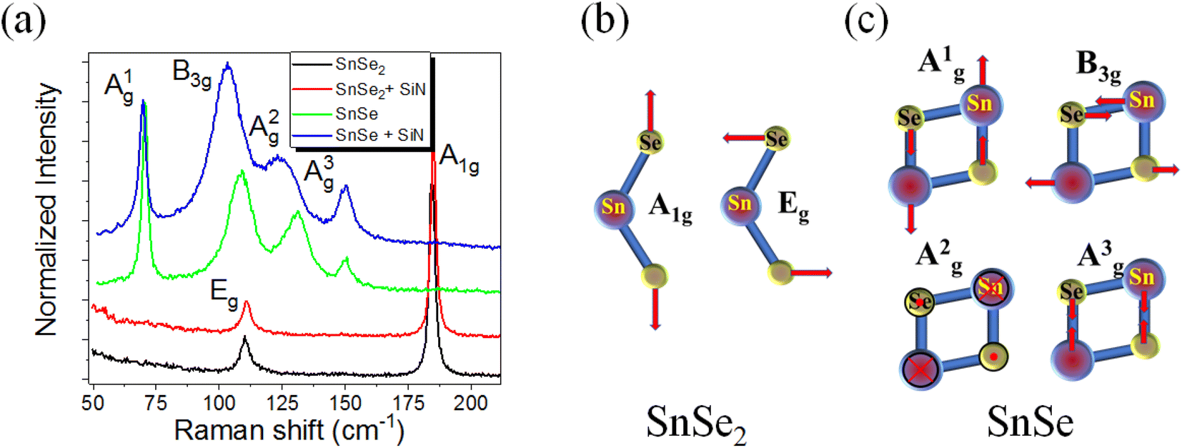 | ||
| Fig. 2 (a) Micro-Raman spectra of the reference sample obtained from the as-exfoliated SnSe2 and SnSe flakes transferred onto an SiNx/Si substrate and capped with a 6 nm-thick SiNx film. All spectra were intentionally shifted along the vertical axis for clarity. Panels (b) and (c) show the atomic displacement corresponding to all Raman-active phonon modes in SnSe2 and SnSe, respectively. | ||
The unit cell of SnSe2 contains one Sn atom and two Se atoms, which means that nine vibrational modes are expected; two acoustic phonon modes, four optical modes of which A1g + Eg are Raman-active, and two more A2u + Eu infrared-active modes. The Raman-active modes are the in-plane Eg at 118 cm−1, indicating that our SnSe2 is composed of a 1T phase, and the out-of-plane phonon mode A1g at 185 cm−1 (see Fig. 2a and b). The SiNx capping layer has no influence on the phonon structure of SnSe2. Fig. 3 exemplarily shows the micro-Raman spectra obtained from the SnSe2 flake after NH3 plasma treatment for 10 s at 300 °C with a plasma power of 20 W. The gas pressures in the chamber were fixed at 700 mTorr. For comparison, the Raman spectra obtained from unprocessed SnSe and SnSe2 are shown. In the case of the unprocessed samples, the Raman spectra show the well-known Raman-active phonon modes in both SnSe and SnSe2, such as the one presented in Fig. 2a. However, the Raman spectrum obtained from the SnSe2 flake after NH3 plasma treatment exhibits five well-resolved phonon modes located at 69.7, 98.7, 121.3, 152.2, and 184.2 cm−1. The first four phonon modes have a similar position to the Ag1, B3g, Ag2 and Ag3 phonon modes in SnSe, while the last phonon mode at 184.2 cm−1 overlaps with the Raman-active A1g phonon mode in SnSe2. The Eg phonon mode from SnSe2 is not well visible in the plasma-treated sample due to the overlapping with the B3g and Ag2 phonon modes from SnSe. The coexistence of the SnSe- and SnSe2-related phonon modes in the Raman spectrum suggest that the top layer of the trigonal SnSe2 flake was converted to an orthorhombic SnSe layer during the NH3-plasma treatment. Moreover, the red shift of the main phonon modes of SnSe and the slight broadening of the Ag1 peak (the FWHM increases from 2.9 cm−1 to 4.6 cm−1 after plasma treatment) indicate tensile strain and defect formation in the top layer, e.g. Se vacancies that are created during the conversion from SnSe2 to SnSe. The lattice parameters of trigonal SnSe2 are a = b = 3.81 Å, and c = 6.14 Å, while the lattice parameters of orthorhombic SnSe are a = 11.5 Å, b = 4.15 Å, and c = 4.44 Å.28 Using DFT calculations, Tian et al. showed that the SnSe2–SnSe heterojunction possesses an atomically flat interface with a well-defined rotation angle between the layers influencing the lattice mismatch and strain accumulation in the converted layer.29 The NH3 plasma can be decomposed into different positively charged ions including NHn+(0≤n≤3), H2+, H+ and N+ during processing. To clarify the influence of the different plasma components on the phase transformation process in chalcogenides, the influence of nitrogen plasma on the stability of the SnSe and SnSe2 flakes was also inspected.
 | ||
| Fig. 3 Micro-Raman spectra taken from as-exfoliated SnSe and SnSe2 flakes, and from SnSe2 flakes after NH3 plasma treatment at 300 °C for 10 s with a plasma power of 20 W and a partial pressure of 700 mTorr. | ||
The N2-plasma parameters were the same as those used for the NH3 plasma. According to Raman spectroscopy, the N2-plasma treatment of SnSe2 even for 2 min does not affect the microstructural properties of the flakes (not shown here). This indicates that ionized hydrogen is primarily responsible for the transformation of Sn-dichalcogenide into Sn-monochalcogenide through the formation of volatile hydrogen-chalcogenide molecules. Kim et al. investigated the phase transformation in SnS2 flakes applying an Ar plasma.22 The phase transformation of SnS2 was observed to occur for a plasma power larger than 60 W. It was also shown that phase transformation depends on plasma power and time. For a plasma power of about 140 W, the SnS phase appears after a few seconds, but the plasma treatment with 60 W needs at least 120 s. However, the Ar-plasma-treated surface turned out to be rough, showing a columnar growth of SnS on top of SnS2, which is due to the selective sputtering of the 2D material and not because of the chemical reaction as in our case. A similar phenomenon was observed in works related to the SnS2 heat treatment via laser irradiation. Laser heating causes selective S evaporation and the phase transformation from SnS2 into SnS.30,31 Using an NH3 plasma we can precisely control the thickness of the converted layer and the interface between the dichalcogenide and the monochalcogenide is almost atomically sharp, as shown later by cross-sectional TEM. The NH3 gas dissociates in the plasma chamber into NHn≤3+, H2+, H+ and N+ ions. Hydrogen ions are highly mobile and can easily diffuse into SnSe2. Hydrogen reacts with Se atoms, reducing SnSe2 to SnSe. The released Se–Hx at an elevated temperature diffuses to the surface and tends to form stable but volatile H2Se molecules that are pumped out from the chamber.
Fig. 4a shows a cross-sectional high-resolution TEM image of the vertical p–n junction formed by NH3-plasma-induced phase transformation of SnSe2. In particular, the sample was treated with an NH3 plasma at 300 °C for 10 s. After this plasma process, about 5–10 nm of the top layer of SnSe2 is converted to SnSe with an atomically flat interface between the two materials. Crystalline SnOx is formed on the top of the SnSe layer due to surface oxidation (Fig. 4d). Fig. 4b and c show fast Fourier transforms (FFTs) obtained from the converted and virgin SnSe2 sample regions depicted in Fig. 4a. In particular, the FFTs are described by [031] and [210] zone axis patterns of SnSe and SnSe2, respectively, confirming the successful phase transformation from trigonal dichalcogenide into orthorhombic monochalcogenide by NH3 plasma treatment. Furthermore, from the element distribution from EDX results (as shown in Fig. 4d), it could be found that the amounts of the Se element at the surface were much lower compared with that of Se in the inner layer. This also indicates the successful phase transformation of SnSe2.
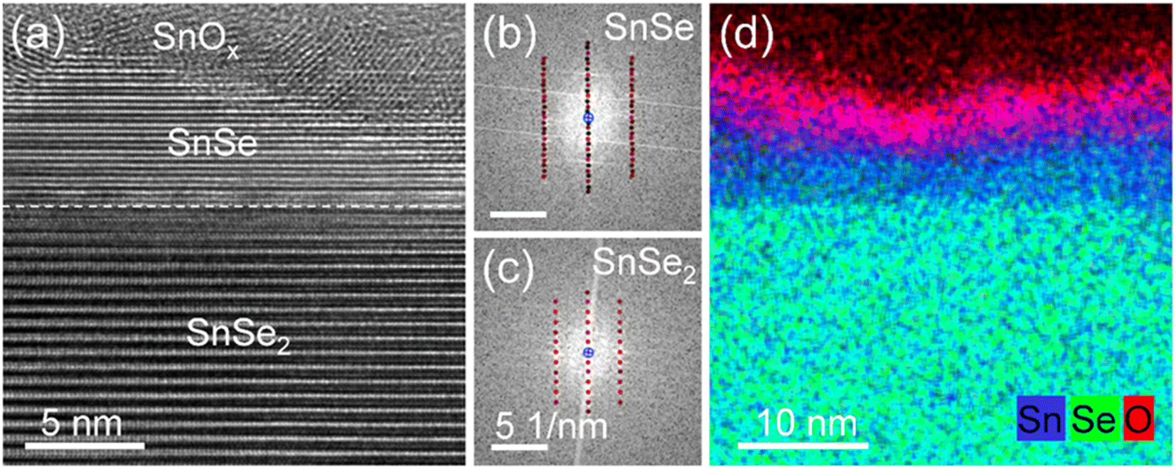 | ||
| Fig. 4 (a) Cross-sectional high-resolution TEM image of a SnSe2 flake after NH3-plasma treatment at 300 °C for 10 s. (b) and (c) fast Fourier transforms obtained from the SnSe and SnSe2 sample regions indicated in panel (a) and superimposed with simulated diffraction patterns of orthorhombic SnSe and trigonal SnSe2 in [031] and [210] zone axis geometry, respectively. (d) Superimposed EDX-based element distributions of Sn (blue), Se (green), and oxygen (red). | ||
Next, we performed an electrical characterization of the SnSe2 flakes before and after NH3-plasma treatment. For this experiment, SnSe2 was exfoliated and subsequently transferred onto a pre-patterned substrate with Au contacts (see upper inset of Fig. 5a). Fig. 5a shows the current–voltage (I–V) curves obtained from an as-deposited SnSe2 flake (black curve) and from a flake after NH3-plasma treatment (red curve). As-grown SnSe2 is an n-type semiconductor with a Fermi level of about 0.02 eV below the conduction band minimum, while the non-intentionally-doped SnSe shows p-type conductivity with a Fermi level of about 0.1 eV above the valence band maximum indicating heavy electron and hole doping, respectively.18,29 It was shown that in both cases Se vacancies are mainly responsible for the doping. Therefore, after the successful transformation of a part of SnSe2 into SnSe, the formation of an n–p junction is expected.
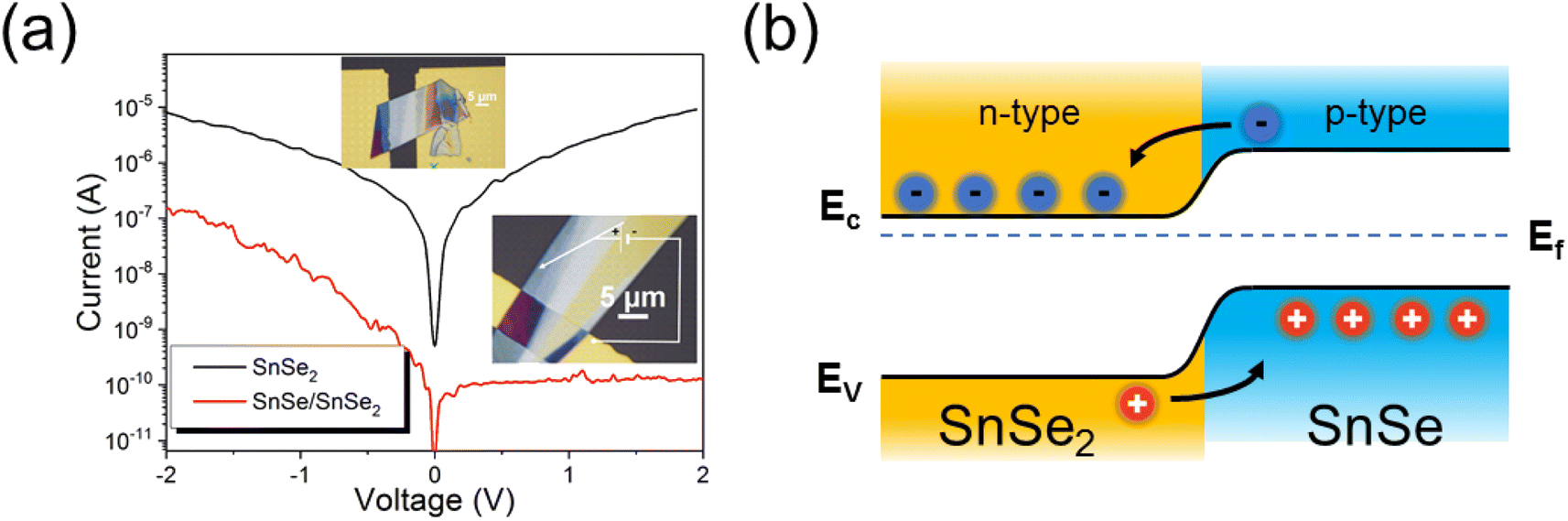 | ||
| Fig. 5 (a) I–V characteristics of an as-exfoliated SnSe2 flake (black curve) and a sample after NH3-plasma treatment. The upper inset shows the SnSe2 flake on gold electrodes, and the bottom inset shows the flake after NH3-plasma treatment with a schematic electrical connection. One electrode is connected to the gold pads and the second one with a needle connects the part of the SnSe2 flake fully transformed into SnSe. (b) Schematic diagram of the band gap alignment for the SnSe/SnSe2 p–n junction. | ||
The current–voltage measurement for the untreated SnSe2 layer shows a typical characteristic for unipolar semiconductors (black curve). The red curve shows the I–V characteristic of the p–n junction made of SnSe/SnSe2. In this case, the thick SnSe2 flake was transferred onto one Au-contact pad only, so that the thicker part of the flake was bonded to the Au-stripe and the thinner part was lying on SiNx. The I–V measurements were performed using a probe station with a microscope in which one probe tip came into contact with the Au-stripe (to connect with SnSe2), while the second probe tip came into contact with p-type SnSe at the end of the flake (see the bottom inset of Fig. 5). Micro-Raman spectroscopy also shows that the blue part of the flake visible in the lower inset of Fig. 5, where the probe tip is touching the flake, contains only SnSe. The I–V curve obtained from the NH3-plasma-treated sample shows typical p–n junction characteristics with a rectification factor in the order of 103 and an ideality factor n = 6.5. An ideality factor above 2 is commonly observed for the 2D heterojunctions due to the interface states and the electrical contact quality between metals and 2D material.32 Optimization of the contact quality was not the focus of the current manuscript. Fig. 5b shows the energy diagram of the SnSe/SnSe2 p–n junction. Taking into account the band offset and the position of the Fermi levels in both semiconductors, the SnSe/SnSe2 p–n junction forms a type-II band alignment.22 The presented I–V curves clearly demonstrate the successful phase transformation of SnSe2 into SnSe and the formation of a p–n junction.
Conclusions
We have demonstrated that n-type SnSe2 flakes can be converted to p-type SnSe flakes using a few seconds of NH3-plasma treatment. The process is precisely controllable and reproducible and leads to an atomically flat SnSe2/SnSe interface. The formed vertical p–n junction shows a rectification factor in the order of 103. The developed method can be used to fabricate both lateral and vertical p–n junctions just by using local masking or adjusting the plasma parameters. The process can be easily scaled up and used to fabricate devices at the wafer scale with different functionalities.Conflicts of interest
There are no conflicts to declare.Acknowledgements
The authors thank Annette Kunz for TEM specimen preparation. Furthermore, the nanofabrication facilities (NanoFaRo) at the HZDR Ion Beam Center, the use of the HZDR Ion Beam Center TEM facilities and the funding of TEM Talos by the German Federal Ministry of Education and Research (BMBF), Grant No. 03SF0451, in the framework of HEMCP are gratefully acknowledged. This work was supported by the Ministry of Science and Technology of Taiwan under contract No. MOST-109-2112-M-006-013 and MOST-110-2124-M-006-010. Yi Li acknowledges the financial support by the Chinese Scholarship Council (File No. 202006890006).References
- L. A. Falkovsky, J. Phys.: Conf. Ser., 2008, 129, 012004 CrossRef.
- Q. H. Wang, K. Kalantar-Zadeh, A. Kis, J. N. Coleman and M. S. Strano, Nat. Nanotechnol., 2012, 7, 699–712 CrossRef CAS PubMed.
- X. Xu, W. Yao, D. Xiao and T. F. Heinz, Nat. Phys., 2014, 10, 343–350 Search PubMed.
- S. Kumar and U. Schwingenschlogl, Chem. Mater., 2015, 27, 1278–1284 CrossRef CAS.
- W. Ai, L. Kou, X. Hu, Y. Wang, A. V. Krasheninnikov, L. Sun and X. Shen, J. Phys.: Condens. Matter, 2019, 31, 445301 CrossRef CAS PubMed.
- W. Jolie, C. Murray, P. S. Weiß, J. Hall, F. Portner, N. Atodiresei, A. V. Krasheninnikov, C. Busse, H.-P. Komsa, A. Rosch and T. Michely, Phys. Rev. X, 2019, 9, 011055 CAS.
- J. R. Schaibley, H. Yu, G. Clark, P. Rivera, J. S. Ross, K. L. Seyler, W. Yao and X. Xu, Nat. Rev. Mater., 2016, 1, 16055 CrossRef CAS.
- A. Chaves, J. G. Azadani, H. Alsalman, D. R. da Costa, R. Frisenda, A. J. Chaves, S. H. Song, Y. D. Kim, D. He, J. Zhou, A. Castellanos-Gomez, F. M. Peeters, Z. Liu, C. L. Hinkle, S.-H. Oh, P. D. Ye, S. J. Koester, Y. H. Lee, P. Avouris, X. Wang and T. Low, npj 2D Mater. Appl., 2020, 4, 29 CrossRef CAS.
- G. Duvjir, T. Min, T. Thi Ly, T. Kim, A.-T. Duong, S. Cho, S. H. Rhim, J. Lee and J. Kim, Appl. Phys. Lett., 2017, 110, 262106 CrossRef.
- J. Jiang, C. P. Y. Wong, J. Zou, S. Li, Q. Wang, J. Chen, D. Qi, H. Wang, G. Eda, D. H. C. Chua, Y. Shi, W. Zhang and A. T. S. Wee, 2D Mater., 2017, 4, 021026 CrossRef.
- P. A. Fernandes, M. G. Sousa, P. M. P. Salomé, J. P. Leitão and A. F. da Cunha, CrystEngComm, 2013, 15, 10278–10286 RSC.
- B. Qin, Y. Zhang, D. Wang, Q. Zhao, B. Gu, H. Wu, H. Zhang, B. Ye, S. J. Pennycook and L.-D. Zhao, J. Am. Chem. Soc., 2020, 142, 5901–5909 CrossRef CAS PubMed.
- Z. Zainal, N. Saravanan, K. Anuar, M. Z. Hussein and W. M. M. Yunus, Mater. Sci. Eng., B, 2004, 107, 181–185 CrossRef.
- N. Okereke and A. Ekpunobi, Chalcogenide Lett., 2010, 7, 531 CAS.
- Y. Xie, H. Su, B. Li and Y. Qian, Mater. Res. Bull., 2000, 35, 459–464 CrossRef CAS.
- D. Martínez-Escobar, M. Ramachandran, A. Sánchez-Juárez and J. S. Narro Rios, Thin Solid Films, 2013, 535, 390–393 CrossRef.
- Z. Zainal, A. J. Ali, A. Kassim and M. Z. Hussein, Sol. Energy Mater. Sol. Cells, 2003, 79, 125–132 CrossRef CAS.
- W. Albers and J. Verberkt, J. Mater. Sci., 1970, 5, 24–28 CrossRef CAS.
- E. Sutter, Y. Huang, H. P. Komsa, M. Ghorbani-Asl, A. V. Krasheninnikov and P. Sutter, Nano Lett., 2016, 16, 4410–4416 CrossRef CAS PubMed.
- T. Zhou, W. K. Pang, C. Zhang, J. Yang, Z. Chen, H. K. Liu and Z. Guo, ACS Nano, 2014, 8, 8323–8333 CrossRef CAS PubMed.
- A. Voznyi, V. Kosyak, L. Grase, J. Vecstaudža, P. Onufrijevs, Y. Yeromenko, A. Medvid’ and A. Opanasyuk, Mater. Sci. Semicond. Process., 2018, 79, 32–39 CrossRef CAS.
- J. H. Kim, S. J. Yun, H. S. Lee, J. Zhao, H. Bouzid and Y. H. Lee, Sci. Rep., 2018, 8, 10284 CrossRef PubMed.
- X. Xu, Q. Song, H. Wang, P. Li, K. Zhang, Y. Wang, K. Yuan, Z. Yang, Y. Ye and L. Dai, ACS Appl. Mater. Interfaces, 2017, 9, 12601–12607 CrossRef CAS PubMed.
- A. Castellanos-Gomez, M. Buscema, R. Molenaar, V. Singh, L. Janssen, H. S. J. van der Zant and G. A. Steele, 2D Mater., 2014, 1, 011002 CrossRef CAS.
- S. Prucnal, A. Hashemi, M. Ghorbani-Asl, R. Hübner, J. Duan, Y. Wei, D. Sharma, D. R. T. Zahn, R. Ziegenrücker, U. Kentsch, A. V. Krasheninnikov, M. Helm and S. Zhou, Nanoscale, 2021, 13, 5834–5846 RSC.
- P. M. Nikolić, L. Milković, P. Mihajlović and B. Lavrenčić, Czech. J. Phys., 1978, 28, 456–459 CrossRef.
- Z. Jian, H. Zhu, X. Wu, H. Cui, D. Li, J. Jiang, C. Gao, Q. Wang and Q. Cui, Nanoscale, 2015, 7, 10807–10816 RSC.
- C. Guillén, J. Montero and J. Herrero, Phys. Status Solidi A, 2011, 208, 679–683 CrossRef.
- Z. Tian, M. Zhao, X. Xue, W. Xia, C. Guo, Y. Guo, Y. Feng and J. Xue, ACS Appl. Mater. Interfaces, 2018, 10, 12831–12838 CrossRef CAS PubMed.
- A. Voznyi, V. Kosyak, P. Onufrijevs, L. Grase, J. Vecstaudža, A. Opanasyuk and A. Medvid’, J. Alloys Compd., 2016, 688, 130–139 CrossRef CAS.
- R. Y. Qi Zheng, K. Wu, X. Lin, S. Du, C. Shen, L. Bao and H.-J. Gao, Chin. Phys. B, 2022, 31, 47306–047306 CrossRef.
- M. Moun, M. Kumar, M. Garg, R. Pathak and R. Singh, Sci. Rep., 2018, 8, 11799 CrossRef PubMed.
| This journal is © The Royal Society of Chemistry 2023 |