DOI:
10.1039/D2NA00713D
(Paper)
Nanoscale Adv., 2023,
5, 1316-1322
Demonstration of programmable light intensity of a micro-LED with a Hf-based ferroelectric ITZO TFT for Mura-free displays
Received
17th October 2022
, Accepted 6th December 2022
First published on 12th December 2022
Abstract
We demonstrate the programmable light intensity of a micro-LED by compensating threshold voltage variability of thin-film transistors (TFTs) by introducing a non-volatile programmable ferroelectric material, HfZrO2 (HZO) into the gate stack of the TFT. We fabricated an amorphous ITZO TFT, ferroelectric TFTs (FeTFTs), and micro-LEDs and verified the feasibility of our proposed current-driving active matrix circuit. Importantly, we successfully present the programmed multi-level lighting of the micro-LED, utilizing partial polarization switching in the a-ITZO FeTFT. We expect that this approach will be highly promising for the next-generation display technology, replacing complicated threshold voltage compensation circuits with a simple a-ITZO FeTFT.
Introduction
Mini- and micro-LED displays have attracted strong attention due to their potential to provide low power consumption, high brightness, high contrast, etc.1,2 Some products have already been commercialized, but there are still lots of technical issues to be solved to utilize their full potential. Specifially, for implementing the display's active matrix current-driving pixels, it is important to fabricate uniform and stable thin-film transistors (TFTs). The conventional amorphous silicon (a-Si) TFTs show uniform electrical characteristics but have low electron mobility and unstable operation.3 The low-temperature polycrystalline silicon (LTPS) TFTs have high electron mobility and stability, but the uniformity in the fabrication process is not sufficient due to grain boundary problems arising from the crystallization process,4 whereas amorphous oxide semiconductor (AOS) TFTs exhibit stable operation, high mobility, and low leakage current even when fabricated at room temperature.5–9 Although AOS TFTs show relatively more stable operation than a-Si and LTPS TFTs, the Vth variation issue still needs to be addressed, resulting in an uneven brightness distribution on the display panel, called the Mura phenomenon. Indeed, a micro-LED display also suffers from the not sufficient uniformity of the pixel itself because the epitaxial growth of the LED layer has been devoted to providing a good figure-of-merit (FoM) for general light applications, but the FoM criteria for the display has turned out to be much severe and tight, especially in terms of the uniformity. Therefore, very sophisticated uniformity compensation in driving circuits has become more important. To reduce the Vth variation, additional compensation circuits are generally used. However, it requires additional elements and access to the driver TFT within the pixel cell, which leads to a complicated and big pixel cell size.10–17
On the other hand, it was reported that a ferroelectric field effect transistor (FeFET) enables the Vth control and memorize the changed states of a transfer curve, which is a reconfigurable and non-volatile memory behavior.18 In 2011, ferroelectricity in hafnium oxide thin films was first reported. Unlike conventional ferroelectric perovskites such as PZT, BTO, and SBT,19 HfO2-based ferroelectrics, which can be formed by atomic layer deposition (ALD)20 and chemical vapor deposition (CVD),21 are highly compatible with Si complementary metal oxide semiconductor (CMOS) technology.22 Since then, many materials such as Zr, Y, Al, Gd, Sr, and La have been studied as dopants,23–25 and it is well-known that Zr with a structure similar to that of Hf can provide a wider composition window where ferroelectricity is obtained in the HfO2-based oxide. In addition, the Zr-doped HfO2-based ferroelectric material, HfZrO2 (HZO) shows a long retention time, low power consumption, and fast switching response.26 Because of these advantages in programming the polarization of ferroelectric HfZrO2, many studies have been conducted on multi-level FeFETs for artificial neural networks and non-volatile memory applications in Si CMOS technology.27–31
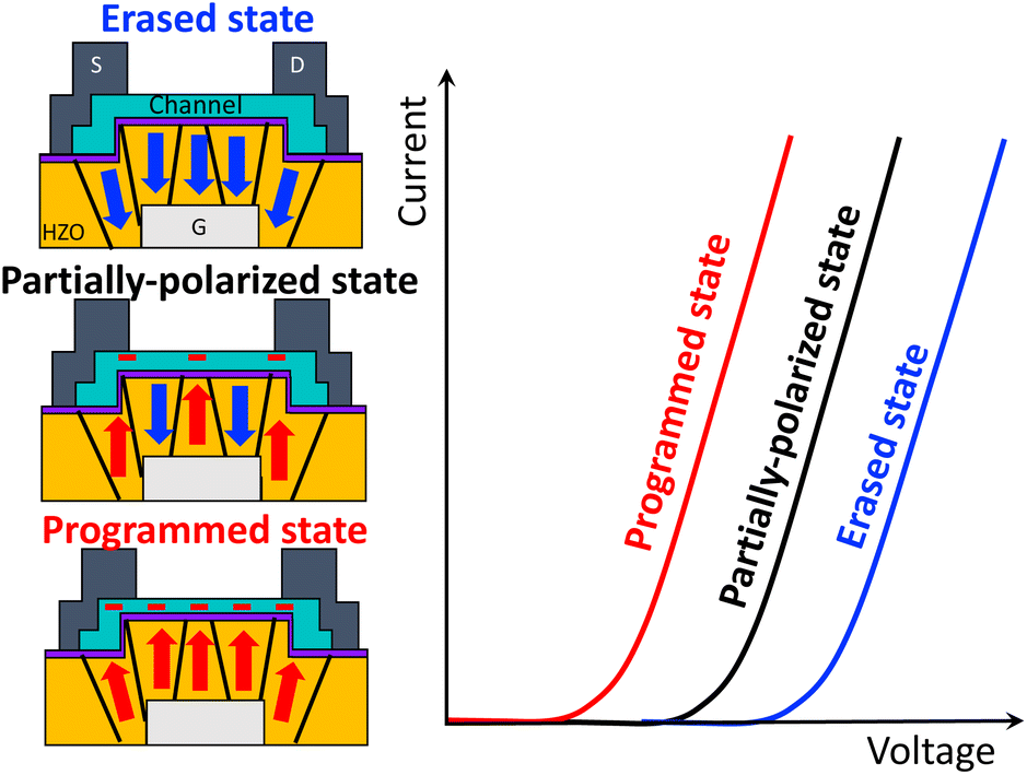
On top of that, David Lehninger et al. studied ferroelectric thin-film transistors (FeTFTs) for potential Vth compensation in display applications.32 However, feasible implementation with display pixels or circuits has not been explored, although it is very timely and important. Fig. 1 shows the multi-level operation principles of FeTFTs for the Vth compensation. The HfO2-based ferroelectric materials are mostly polycrystals and have a very large number of spontaneously polarized grains below the Curie temperature. Each grain contains several domains and thus has a different coercive field.33–35 That is, the number of polarization domains determining the Vth of the TFT channel can be controlled by adjusting the amplitude, width, and the number of applied pulse voltages as depicted in Fig. 1. In this work, we demonstrate the programmable light intensity of a micro-LED by using an active matrix current-driving display pixel that compensates for such variabilities using partial polarization switching and non-volatile behavior in a HfO2-based FeTFT, as shown in Fig. 2. For the first time, we experimentally show multi-level light output power operations of micro-LEDs, driven by the fabricated amorphous In–Sn–Zn–O (a-ITZO) FeTFT with a programmable ferroelectric HZO gate stack.
 |
| | Fig. 1 Schematic operation principles of the Vth compensation using a FeTFT. | |
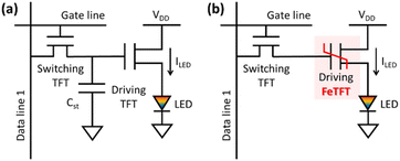 |
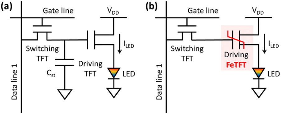
| | Fig. 2 (a) Conventional and (b) proposed current driving active-matrix circuits for displays. | |
Device fabrication
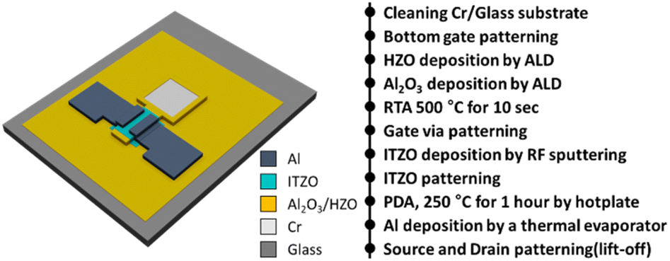
We fabricated Al/a-ITZO/Al2O3/HZO/Cr FeTFTs for the driving FeTFT and Al/Al2O3/HZO/Cr ferroelectric capacitors for the ferroelectricity study, simultaneously. Fig. 3 shows the fabrication process flow of a-ITZO FeFETs and ferroelectric capacitors. First, a Cr (50 nm)/glass substrate was wet cleaned, followed by bottom Cr gate electrode formation. Then, nano-laminated Al2O3 (1 nm)/HZO (10 nm) was deposited by ALD36,37 and patterned by photolithography. The Al2O3 capping layer was added to prevent inter-diffusion between the HZO and a-ITZO,32 pursuing a high-quality MOS interface, predominantly to affect the endurance characteristics of the FeFETs. Furthermore, this would be helpful to form a non-centrosymmetric o-phase in HZO38,39 and to achieve a large coercive field or memory window.40 The sample was annealed at 500 °C for 10 s by rapid thermal annealing to enhance ferroelectricity in HZO,41 after gate via patterning. The annealing temperature of 500 °C is higher than the thermal budget of ∼400 °C for conventional TFT technology. Recent studies show that such low-temperature processes for deposition and annealing below 400 °C are sufficient to crystallize HZO films.42–44 Therefore, it will be compatible with TFT technologies. An a-ITZO (7 nm) channel layer was deposited by using an RF sputter and patterned in the same way. Finally, source and drain electrodes with Al (50 nm) were constructed by using a thermal evaporator. We also fabricated a-ITZO FETs as a switching FET. Most of the processes are the same, but a 10-nm-thick Al2O3 layer was deposited by ALD instead of Al2O3 (1 nm)/HZO (10 nm) in the FeFET fabrication process.
 |
| | Fig. 3 Schematic device structure and process flow of a HZO ferroelectric TFT. | |
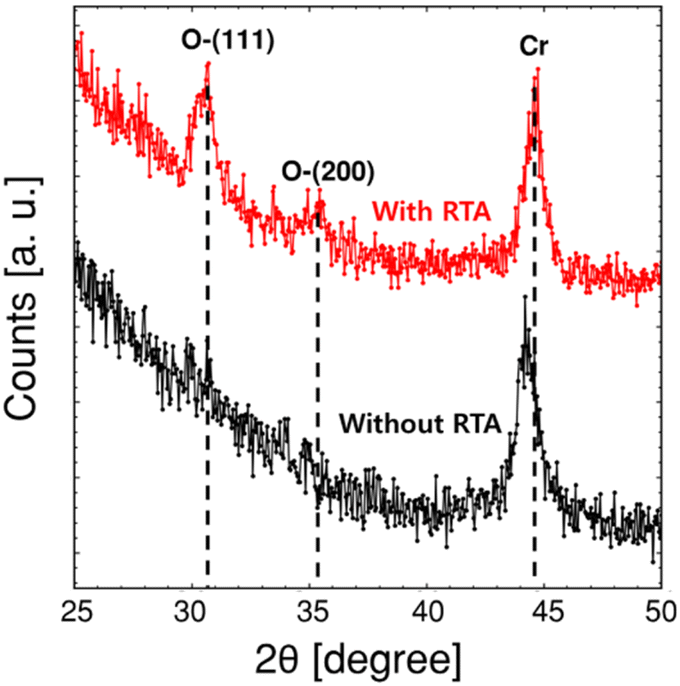
To confirm the fabricated devices, transmission electron microscopy (TEM), scanning transmission electron microscopy (STEM), and energy-dispersive X-ray spectroscopy (EDS) images were obtained by using a Tecnai F20 G2 and Titan™ 80-300 as shown in Fig. 4. We confirmed the channel and source/drain regions of the FeTFT structure as shown in Fig. 4(a). To verify the crystal quality of HZO and ITZO, high-resolution TEM and STEM were also obtained as shown in Fig. 4(b) and (c). There is no significant interfacial layer between a-ITZO and Al2O3/poly-crystalized HZO in the figures unlike the HZO/Si interface.37 This will lead to some advantages compared to a Si FeFET as will be discussed later. Significantly, a nano-laminated HZO structure was also observed in the STEM image. The separated layer structure of the a-ITZO/Al2O3/HZO/Cr/glass substrate FeTFT was shown in the EDS analysis. Sn and Zn have relatively large noise due to the artificial signal of Pt and Ga injected by the focused ion beam process for TEM sampling. To confirm the presence of a non-centrosymmetric orthorhombic phase, X-ray diffraction (XRD) was performed by using a RIGAKU D/MAX2200. As shown in Fig. 5, with RTA, the intensity of the orthorhombic/tetragonal/cubic manifold phase peak (o/t/c) (2θ ≃ 30.5 degrees) increased significantly, but the intensity of the monoclinic phase (m) (2θ ≃ 28.5 degrees) hardly increased. The XRD data could be used to confirm that a stabilized o-phase existed.
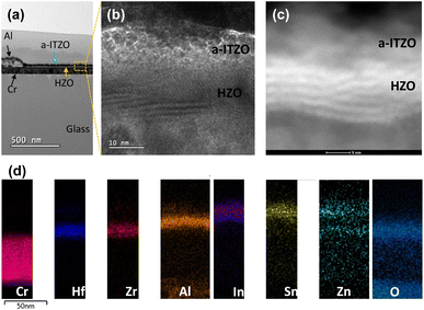 |
| | Fig. 4 (a) TEM image of S/D and channel regions. (b) TEM, (c) STEM, and (d) EDS images of an a-ITGO/Al2O3/HZO/Cr FeFET. | |
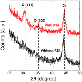 |
| | Fig. 5 XRD pattern of the HZO film with RTA and without RTA. | |
Measurement results & discussion
A Switching thin-film transistor using Al2O3 and a-ITZO
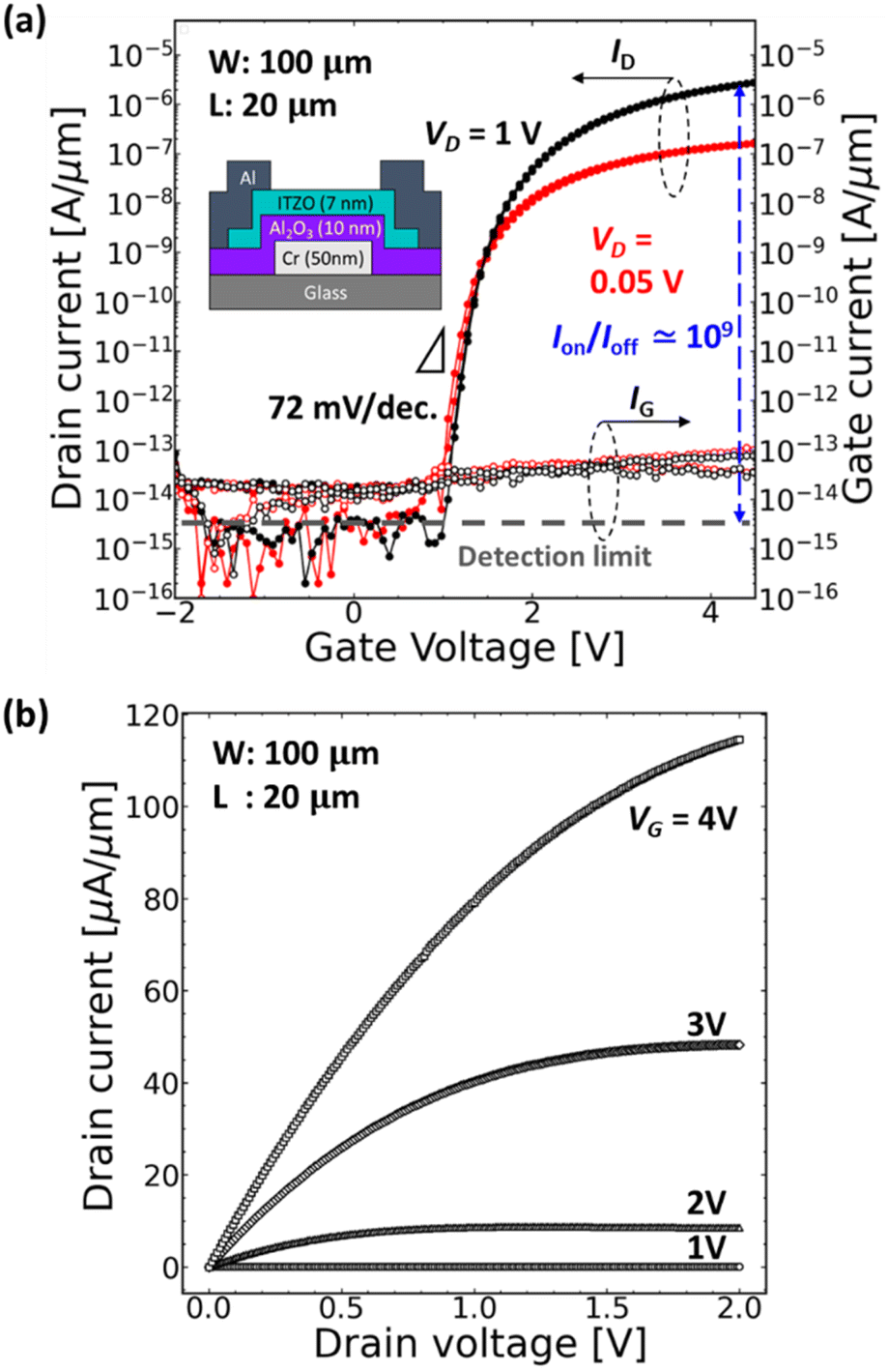
First, to investigate the transport characteristics of a-ITZO TFTs, we measured the electrical properties of the fabricated a-ITZO TFTs. Fig. 6(a) and (b) show the drain current–gate voltage (ID–VG), and the drain current–drain voltage (ID–VD) characteristics of the fabricated a-ITZO TFTs. The electrical performance measurements were carried out with a parameter analyzer (Agilent 4155C). The ID–VG characteristics of a-ITZO TFT are shown in Fig. 6(a). The VD is fixed at 1 V, and 0.05 V respectively, while the VG is swept from −2 V to 4.5 V and then back to −2 V. As presented in Fig. 6(a), the ID–VG shows a very good transfer curve. The curves show a negligible hysteresis, meaning no such trap states were present. The a-ITZO TFT also shows excellent electrical performances like low leakage current (<1015 A μm−1), a large current on–off ratio (≃109), and saturated field-effect mobility (≈5.30 cm2 V−1 s−1) with an insulator capacitance of 480 nF cm−2 and steep subthreshold swing (72 mV dec−1). Therefore, the a-ITZO TFT can be used for a stable switching device in the proposed circuit. The ID–VD characteristics of the a-ITZO TFT were also measured as shown in Fig. 6(b). The VG is biased from 0 V to 4 V and increases by 1 V per step. It also shows good current saturation under high VD conditions with remarkable transconductance behaviors.
 |
| | Fig. 6 (a) ID–VG and (b) ID–VD characteristics of the Al2O3 TFT. | |
B Driving a ferroelectric thin-film transistor using ferroelectric HZO and a-ITZO
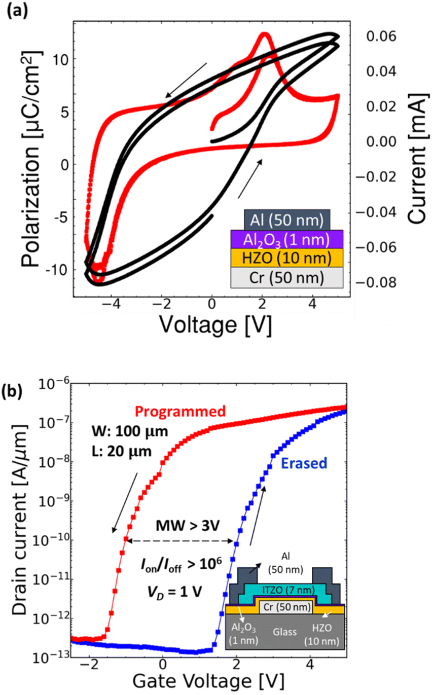
To evaluate the memory characterization of the device, we examined the ferroelectric characteristics of the metal–ferroelectric–metal (MFM) capacitors and the FeFETs. Fig. 7(a) shows the polarization–voltage (P–V) and current–voltage (I–V) curves of the Al/Al2O3/HZO/Cr MFIM capacitor. The ferroelectricity of the capacitor was characterized with a FE analyzer (Precision LC II) using a triangular waveform at a frequency of 1 kHz. The VG was swept from −5 V to 5 V and then back to −5 V. The polarization–voltage curve of the stack shows counterclockwise hysteresis during the sweep, indicating the ferroelectricity of HZO. The remanent polarization, Pr is about 6.5 μC cm−2 with a 5 V sweep. The positive coercive field of the stack, +Ec is about 1.0 MV cm−1, and the negative coercive field of the stack, −Ec is about −3.6 MV cm−1. The asymmetry of the coercive field is caused by the non-symmetric metal–ferroelectric–insulator–metal (MFIM) stack45 and the different work functions.46 A relatively low Pr, compared to that in the previous report32 was observed. It has been caused by the post-deposition annealing of HZO without a top metal layer, contributing to low mechanical stress in the HZO film and so low generation of o-phase in the film;47 therefore, further improvements are still possible after the development of the post-metallization annealing process with ITZO and HZO. We fabricated a FeTFT with the same gate stack based on these ferroelectric characteristics. Fig. 7(b) shows the ID–VG characteristics of the fabricated a-ITZO FeTFT. The VD is fixed at 1 V, while the VG is swept from −2.5 V to 6 V and then back to −2.5 V.
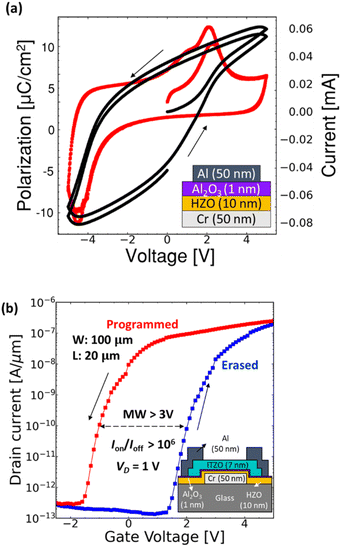 |
| | Fig. 7 (a) Polarization–voltage (P–V) hysteresis and current–voltage (I–V) curves of the Cr/HZO/Al2O3/Al MFIM capacitor and (b) ID–VG characteristics of the a-ITZO FeTFT. | |
The round-trip ID–VG curve shows a large counterclockwise hysteresis curve. Hysteresis can be caused by charge trapping, which is normally clockwise for an n-channel FET. However, our fabricated n-type a-ITZO FeTFT in Fig. 7(b) shows a counterclockwise, which clearly indicates a ferroelectricity-induced hysteresis curve. The memory window (MW) can be extracted according to the following expression:
where
Ec is the coercive field (∼2.3 MV cm
−1),
tF is the thickness of the ferroelectric layer (10 nm), and
α is a parameter that has a weak dependence on the polarization
P and the dielectric constant of the ferroelectric
εF,
40 which is generally lower than 1.
48 The MW of the stack is estimated to be approximately 3 to 4 V using
eqn (1), which is close to the experimental value.
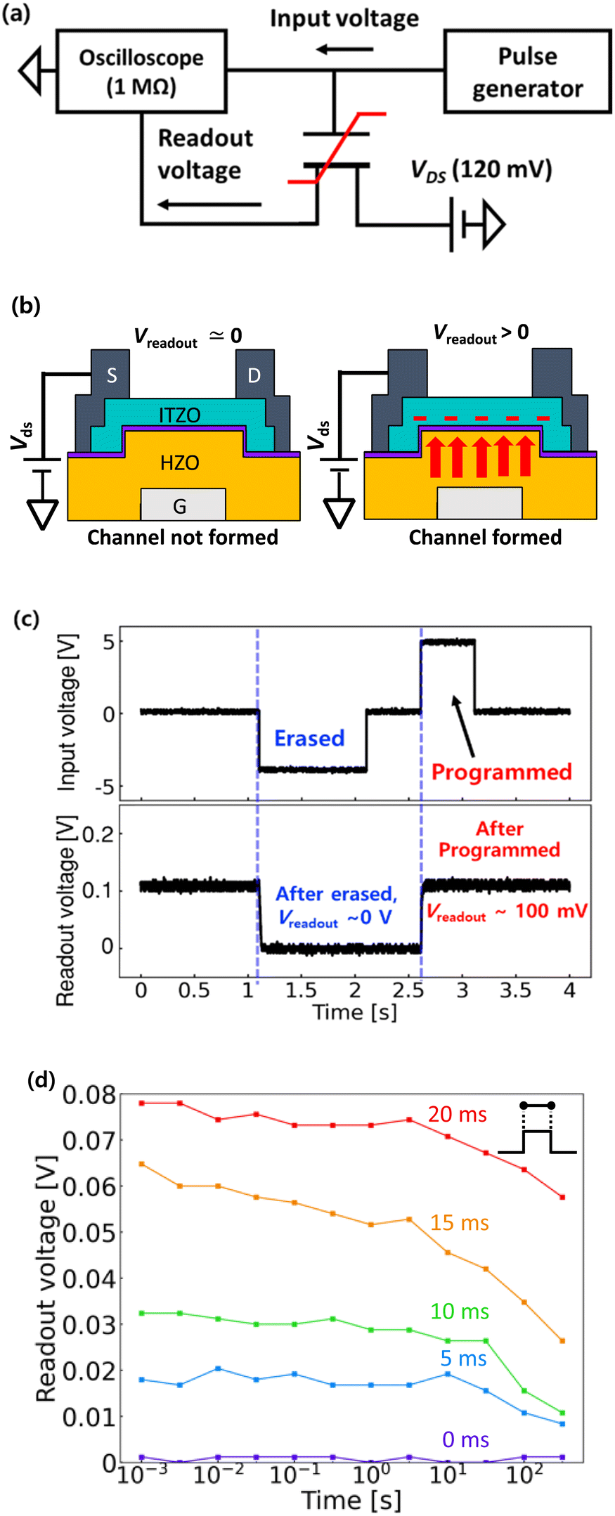
We examined the programming and erasing operation of the fabricated a-ITZO FeTFT. The measurement setup of the block diagram to evaluate the programmability of the fabricated a-ITZO FeTFT is illustrated in Fig. 8(a). Fig. 8(b) shows a schematic device cross-section of erased (channel not formed, Vreadout = 0 V) and programmed (channel formed, Vreadout > 0 V) states. The VD was set to be 120 mV, to avoid the stress applied to the device as much as possible, and the resistance of the oscilloscope was 1 MΩ. Here, the readout voltage is the voltage between the source electrode of the FeFET and the oscilloscope. Since the negative coercive field is larger than the positive coercive field, the erase pulse width is larger than the program pulse width. As shown in Fig. 8(c), after applying the erase pulse (−5 V, 1.5 s) to the bottom gate electrode, the readout voltage was 0 V corresponding to the erased state, and after applying the programmed pulse (5 V, 1 s), the readout voltage was up to 100 mV corresponding to a programmed state. According to the report by Lehninger et al.,32 the negative pulse or electric field is not efficiently applied to the HZO in the gate stack without an additional top or back gate. Like the a-IGZO TFT in the reference, it is also difficult to obtain inversion of the a-ITZO TFT. Nevertheless, we observed the erasing operation in the a-ITZO FeTFT. It would be caused by charge trapping assisted polarization switching. As previously reported by Kuk et al.,37,49 the nFeFET can operate by only electron trapping/de-trapping without holes, which would be like this a-ITZO FeTFT case.
 |
| | Fig. 8 (a) Block diagram of the measurement setup. (b) Schematic diagram when the channel is not formed or formed. (c) Input and readout voltage vs. time. (d) Retention properties with various pulse times. | |
In addition, the remnant polarization value of the MFIM stack is relatively small (Pr = 6.5 μC cm−2). As a result, the required electric field for polarization switching will be lower than that for a larger Pr case. Therefore, it would attribute the erasing ability despite the lack of holes in a-ITZO. We also measured the readout voltage with various pulse widths from 0 to 20 ms for multi-level operation as shown in Fig. 8(d). As the pulse width increases, the readout voltage gradually increases because partial switching of the ferroelectric domain moderately shifts the threshold voltage of a-ITZO FeTFTs. Therefore, the fabricated a-ITZO FeTFT can demonstrate clearly separated multi-level readout voltages using partially switched states in the ferroelectric HZO films. These results strongly show that the fabricated FeTFT is programmable and erasable. Although the retention property shows degradation as the time increases from 10 s at this moment, our devices showed immediate read-after-program from 10−3 s, which is typically very difficult to achieve in Si channel FeFETs due to the charge trapping associated with the interfacial layer between HZO and the channel.37,49 Retention characteristics can be further improved by optimizing the ferroelectric gate stack of metal/HZO/a-ITZO.
C Programmed multi-level operation of a micro-LED by using a FeTFT
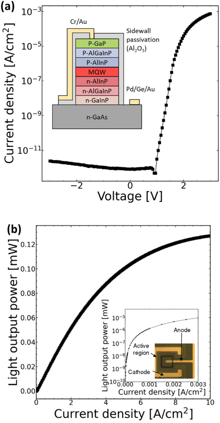
In this section, we demonstrate programmable multi-level lighting for light power compensation to ultimately avoid the Mura effect, based on the multi-level operation of FeTFTs. For the light source, we fabricated AlGaInP/GaInP red micro-LEDs, a highly promising device for next-generation display technology. The details on the micro-LED are found in ref. 50. Fig. 9(a) shows the electrical characteristics of a micro-LED with dimensions of 20 × 20 μm2. Also, the inset of Fig. 9(a) shows the schematic cross-sectional device of the red LED. The rectifying characteristics were shown, indicating a well-formed pn-junction diode. The leakage current is well suppressed to be lower than 10−11 A cm−2 due to a well-controlled sidewall surface and subsequent sidewall passivation.50Fig. 9(b) shows the light output power as a function of injected current with a linear scale and the log scale of it is shown in the inset, including the top view of the fabricated LED. As the injected current density increases, the light output power increases and becomes saturated similar to that of the conventional LEDs. The light output power region in the log scale graph in the inset is the low current density region, corresponding to the programmed multi-level lighting demonstration later.
 |
| | Fig. 9 (a) Current density–voltage characteristics and (b) light output power–current density characteristics of AlGaInP/GaInP MQW LEDs with various device sizes. | |
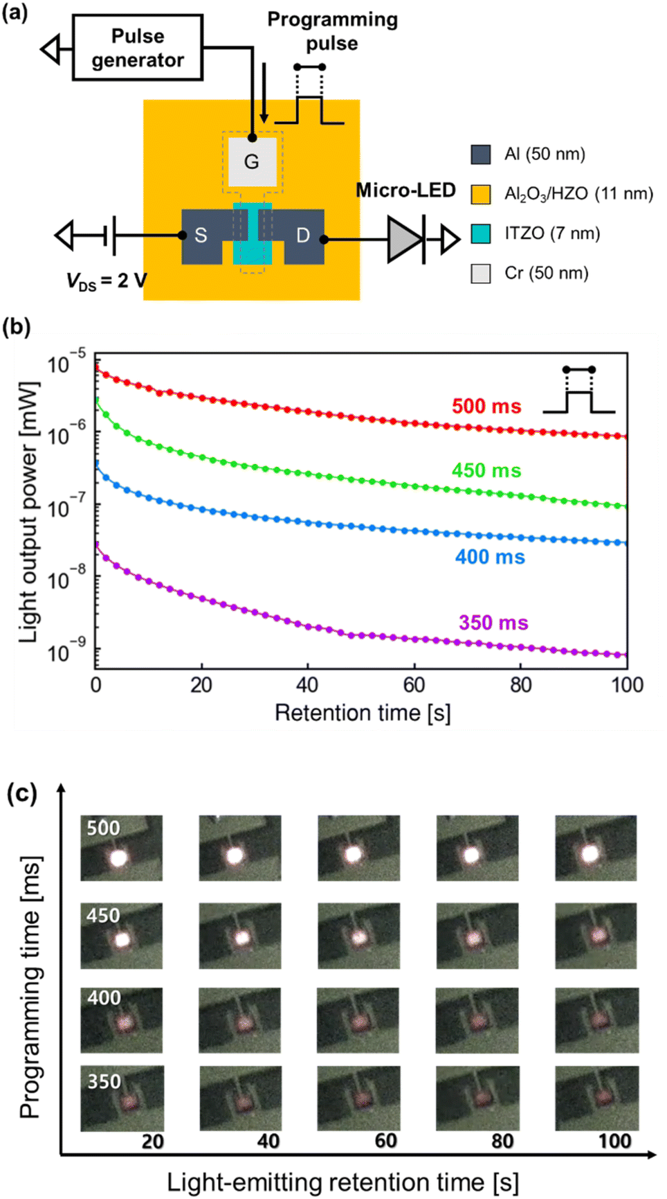
Fig. 10(a) illustrates the measurement setup of the multi-level operation of the micro-LED, programmed by using the FeTFT. The programming pulses (6 V, 350 to 500 ms) were applied to the gate electrode of the FeTF, to light up the micro-LED, a VDS of 2 V was applied, and the source electrode was electrically connected to the anode of the micro-LED. On increasing the pulse width, the light output power also increases as shown in Fig. 10(b). The four multi-level lightings were successfully programmed by using the fabricated FeTFT, indicating that light output power can be adjusted by using the Vth compensation at the device level using the partial polarization behavior in the a-ITZO FeTFT. The four lighting levels are retained for more than 100 s as clear as the four levels are distinguishable. The programming time is relatively long regarding a frame rate. Also, the retention property would not last long enough because the fabricated FeTFT has not been optimized yet. However, recent studies show a very fast program time of fewer than 1 μs, and a retention time of close to 104 s.51 Therefore, achieving a much faster program time than a frame rate will be possible, by maintaining a certain light intensity. The Vth shift could have occurred due to the multiple program/erase cycles. On top of that, Fei Mo et al., reported the reliability characteristics of a similar device with HZO and an oxide semiconductor. Their endurance result shows a slight Pr reduction due to the stress of multiple program/erase cycles, but up to 108 cycles of program/erase is achieved. Therefore, the Vth shift would be suppressed with further optimization. On the other hand, the Vth shift due to the stress would possibly be compensated by the programmability of the FeTFT. This is indeed an interesting advantage of this approach. Fig. 10(c) shows the top-view images of the programmed lighting micro-LEDs, which visualize distinguishable light emissions by changing the program pulse width and its retention.
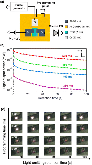 |
| | Fig. 10 (a) Block diagram of the measurement setup, (b) light output power of an AlGaInP micro-LED with four programmed multi-levels vs. retention time, and (c) its top-view images pictured by using a CCD camera during lighting. | |
Conclusions
In conclusion, we demonstrate the programmable light intensity of a micro-LED by using a FeTFT for Mura-free displays. We fabricated a-ITZO TFTs, FeTFTs, and micro-LEDs, showing superior device performances. Notably, we experimentally present the multi-level light output power of the micro-LED, electrically connected, and programmed by using partial polarization switching in the a-ITZO FeTFT. We expect that this approach will be highly promising for the next display technology, replacing complicated Vth compensation circuits with a FeTFT.
Author contributions
TJ, XS, TN, CK, JP, SK, and YK were involved in the experiments. TJ, SA, TN, DA, JP, JH, SK, and YK participated in analysis and discussions. DA and JH contributed to the preparation of ferroelectric HZO samples and their analysis. TJ, SA, DA, JH, SK, and YK drafted the manuscript. All authors read and approved the final manuscript.
Conflicts of interest
There are no conflicts to declare.
Acknowledgements
This work was supported by the research fund of Hanyang University (HY-2022-2566). We would like to thank Prof. Jaekyun Kim, Prof. Dong-Soo Shin, and Prof. Bo Soo Kang of Hanyang University ERICA for their support in the device fabrication and measurement.
References
- I. Piquero-Zulaica,
et al.
, Nanoscale, 2019, 11(48), 23132–23138 RSC
 .
.
- Z. Chen, S. Yan and C. Danesh, J. Phys. D: Appl. Phys., 2021, 54(12), 123001 CrossRef CAS .
- M. J. Powell, C. Van Berkel and J. R. Hughes, Appl. Phys. Lett., 1989, 54(14), 1323–1325 CrossRef CAS .
- T. Urabe, T. Sasaoka, K. Tatsuki and J. Takaki, SID Symposium Digest of Technical Papers, 2007, 38(1), 161–164 CrossRef CAS .
- K. Nomura, H. Ohta, A. Takagi, T. Kamiya, M. Hirano and H. Hosono, Nature, 2004, 432, 488 CrossRef CAS PubMed .
- W. Lim, S.-H. Kim, Y.-L. Wang, J. W. Lee, D. P. Norton, S. J. Pearton and I. I. Kravchenko,
et al.
, J. Vac. Sci. Technol., B: Microelectron. Nanometer Struct., 2008, 26(3), 959 CrossRef CAS .
- Y. Kwon, Y. Li, Y. W. Heo, M. Jones, P. H. Holloway, D. P. Norton and S. Li,
et al.
, Appl. Phys. Lett., 2004, 84(14), 2685–2687 CrossRef CAS .
- R. L. Hoffman, B. J. Norris and J. F. Wager, Appl. Phys. Lett., 2003, 82(5), 733–735 CrossRef CAS .
- K. Nomura, H. Ohta, K. Ueda, T. Kamiya, M. Hirano and H. Hosono, Science, 2003, 300(5623), 1269–1272 CrossRef CAS PubMed .
- S. Ono, K. Miwa, Y. Maekawa and T. Tsujimura, IEEE Trans. Electron Devices, 2007, 54(3), 462–467 CAS .
- J. P. Lee, J. Y. Hwang and B. S. Bae, J. Semicond. Technol. Sci., 2014, 14(5), 594–600 CrossRef .
- Y. Kim, Y. Kim and H. Lee, J. Disp. Technol., 2014, 10(12), 995–1000 Search PubMed .
- Y. Matsueda, D.-Y. Shin and H.-K. Chung, SID Symposium Digest of Technical Papers, 2008, 39(1), 9 CrossRef .
- T. Tsujimura, W. Zhu, S. Mizukoshi, N. Mori, K. Miwa, S. Ono and M. Kohno,
et al.
, SID Symposium Digest of Technical Papers, 2007, 38(1), 84–88 CrossRef CAS .
- S.-K. Hong, B.-K. Kim and Y.-M. Ha, SID Symposium Digest of Technical Papers, 2007, 38(1), 1366–1369 CrossRef .
- Y. Luo and S. Liu, IEEE J. Solid-State Circuits, 2017, 52(8), 2208–2214 Search PubMed .
- I. M. Filanovsky and A. Allam, IEEE Transactions on Circuits and Systems I: Fundamental Theory and Applications, 2001, 48(7), 876–884 CrossRef .
- R. Zuleeg and H. H. Wieder, Solid-State Electron., 1966, 9, 657–661 CrossRef .
- C.-U. Pinnow and T. Mikolajick, J. Electrochem. Soc., 2004, 151(6), K13–K19 CrossRef CAS .
- S. Zarubin, E. Suvorova, M. Spiridonov, D. Negrov, A. Chernikova, A. Markeev and A. Zenkevich, Appl. Phys. Lett., 2016, 109, 192903 CrossRef .
- J. Müller, T. S. Böscke, U. Schröder, S. Mueller, D. Bräuhaus, U. Böttger, L. Frey and T. Mikolajick, Nano Lett., 2012, 12, 4318 CrossRef PubMed .
- T. S. Böscke, J. Müller, D. Bräuhaus, U. Schröder and U. Böttger, Appl. Phys. Lett., 2011, 99(10), 102903 CrossRef .
- J. Müller,
et al.
, IEEE Int. Electron Devices Meet., 2013, 10.8.1–10.8.4 Search PubMed .
- M. H. Park, Y. H. Lee, H. J. Kim, Y. J. Kim, T. Moon, K. D. Kim, J. Müller, A. Kersch, U. Schroeder, T. Mikolajick and C. S. Hwang, Adv. Mater., 2015, 27, 1811 CrossRef CAS PubMed .
- J. Müller, P. Polakowski, S. Mueller and T. Mikolajick, ECS J. Solid State Sci. Technol., 2015, 4, N30 CrossRef .
- S. J. Kim, J. Mohan and S. R. Summerfelt,
et al.
, JOM, 2019, 71, 246–255 CrossRef CAS .
- M. Bohr, R. Chau, T. Ghani and K. Mistry, IEEE Spectrum, 2007, 44, 29–35 Search PubMed .
- T. Ali, R. Olivo, M. Lederer, R. Hoffmann, P. Steinke, K. Zimmermann and F. Muller,
et al.
, Tech. Dig. - Int. Electron Devices Meet., 2019, 2–5 Search PubMed .
- H. Mulaosmanovic, S. Slesazeck, J. Ocker, M. Pesic, S. Muller, S. Flachowsky and T. Mikolajick,
et al.
, Tech. Dig. - Int. Electron Devices Meet., 2015, 26.8.1–26.8.3 Search PubMed .
- S. K. Hwang, I. Bae, S. M. Cho, R. H. Kim, H. J. Jung and C. Park, Adv. Funct. Mater., 2013, 23(44), 5484–5493 CrossRef CAS .
- S. Oh, T. Kim, M. Kwak, J. Song, J. Woo, S. Jeon and H. Hwang,
et al.
, IEEE Electron Device Lett., 2017, 38(6), 732–735 CAS .
- D. Lehninger, M. Ellinger, T. Ali, S. Li, K. Mertens, M. Lederer and K. Seidel,
et al.
, Adv. Electron. Mater., 2021, 2100082 CrossRef CAS .
- W. Cao and C. A. Randall, J. Phys. Chem. Solids, 1996, 57(10), 1499–1505 CrossRef CAS .
- S. Choudhury, Y. L. Li, C. Krill and L. Q. Chen, Acta Mater., 2007, 55(4), 1415–1426 CrossRef CAS .
- J. Y. Li, R. C. Rogan, E. Üstündag and K. Bhattacharya, Nat. Mater., 2005, 4(10), 776–781 CrossRef CAS PubMed .
-
S.-M. Han, D.-W. Rho, D.-H. Ahn, J.-D. Song, W.-Y. Choi and J.-H. Han, Optical Fiber Communications Conference and Exhibition, OFC, 2021, pp. 1–3 Search PubMed .
- S.-H. Kuk, S.-M. Han, B. H. Kim, S.-H. Baek, J.-H. Han and S.-H. Kim, IEEE Trans. Electron Devices, 2022, 69(4), 2080–2087 CAS .
- B. Liu, Y. Cao, W. Zhang and Y. Li, Appl. Phys. Lett., 2021, 119, 172902 CrossRef CAS .
- J. Wang, M. Qin, M. Zeng, X. Gao, G. Zhou, X. Lu, J. M. Liu, D. Wang, Q. Li, A. Zhang, D. Gao, M. Guo, J. Feng, Z. Fan and D. Chen, IEEE Electron Device Lett., 2019, 40(12), 1937–1940 CAS .
- H.-T. Lue, C.-J. Wu and T.-Y. Tseng, IEEE Trans. Electron Devices, 2002, 49(10), 1790–1798 CrossRef .
- M. H. Park,
et al.
, Appl. Phys. Lett., 2013, 102, 112914 CrossRef .
- D. Lehninger, R. Olivo, T. Ali, M. Lederer, T. Kämpfe, C. Mart, K. Biedermann, K. Kühnel, L. Roy, M. Kalkani and K. Seidel, Phys. Status Solidi A, 2020, 217, 1900840 CrossRef CAS .
- T. Onaya, T. Nabatame, N. Sawamoto, A. Ohi, N. Ikeda, T. Nagata and A. Ogura, Microelectron. Eng., 2019, 215, 111013 CrossRef CAS , ISSN 0167-9317.
- H.-B. Kim,
et al.
, Nanoscale, 2021, 13, 8524–8530 RSC .
- M. Lederer, R. Olivo, D. Lehninger, S. Abdulazhanov, T. Kämpfe, S. Kirbach, C. Mart, K. Seidel and L. M. Eng, Phys. Status Solidi RRL, 2021, 15, 2100086 CrossRef CAS .
- M. H. Park, H. J. Lee, G. H. Kim, Y. J. Kim, J. H. Kim, J. H. Lee and C. S. Hwang, Adv. Funct. Mater., 2011, 21, 4305–4313 CrossRef CAS .
- R. Cao,
et al.
, IEEE Electron Device Lett., 2018, 39(8), 1207–1210 CAS .
- H. Mulaosmanovic, E. T. Breyer, T. Mikolajick and S. Slesazeck, IEEE Trans. Electron Devices, 2019, 66(9), 3828–3833 CAS .
- S.-H. Kuk,
et al.
, IEEE Int. Electron Devices Meet., 2021, 33.6.1–33.6.4 Search PubMed .
- J. Park, W. Baek and D. M. Geum, Nanoscale Res. Lett., 2022, 17, 29 CrossRef CAS .
- F. Mo, T. Saraya, T. Hiramoto and M. Kobayashi, Appl. Phys. Express, 2020, 13, 074005 CrossRef CAS .
Footnote |
| † Both authors equally contributed to this work. |
|
| This journal is © The Royal Society of Chemistry 2023 |
Click here to see how this site uses Cookies. View our privacy policy here. 
 Open Access Article
 This Open Access Article is licensed under a Creative Commons Attribution-Non Commercial 3.0 Unported Licence
 a,
Sanghyeon
Kim†
a,
Sanghyeon
Kim†