
 Open Access Article
 This Open Access Article is licensed under a Creative Commons Attribution-Non Commercial 3.0 Unported Licence
Electric dipole modulation for boosting carrier recombination in green InP QLEDs under strong electron injection†
Tianqi
Zhang
abc,
Pai
Liu
bc,
Fangqing
Zhao
bc,
Yangzhi
Tan
bc,
Jiayun
Sun
bc,
Xiangtian
Xiao
bc,
Zhaojing
Wang
bc,
Qingqian
Wang
bc,
Fankai
Zheng
bc,
Xiao Wei
Sun
bc,
Dan
Wu
d,
Guichuan
Xing
 *a and
Kai
Wang
*bc
*a and
Kai
Wang
*bc
aInstitute of Applied Physics and Materials Engineering, University of Macau, Macau, 999078, China. E-mail: gcxing@um.edu.mo
bGuangdong University Key Laboratory for Advanced Quantum Dot Displays and Lighting, Department of Electrical and Electronic Engineering, Southern University of Science and Technology, Shenzhen, 518055, China. E-mail: wangk@sustech.edu.cn
cKey Laboratory of Energy Conversion and Storage Technologies (Southern University of Science and Technology), Ministry of Education, Shenzhen, 518055, China
dCollege of New Materials and New Energies, Shenzhen Technology University, Shenzhen 518118, China
First published on 1st November 2022
Abstract
Enhanced and balanced carrier injection is essential to achieve highly efficient green indium phosphide (InP) quantum dot light-emitting diodes (QLEDs). However, due to the poor injection of holes in green InP QLEDs, the carrier injection is usually balanced by suppressing the strong electron injection, which decreases the radiation recombination rate dramatically. Here, an electric dipole layer is introduced to enhance the hole injection in the green InP QLED with a high mobility electron transport layer (ETL). The ultra-thin MoO3 electric dipole layer is demonstrated to form a positive built-in electric field at the interface of the hole injection layer (HIL) and hole transport layer (HTL) due to its deep conduction band level. Simulation and experimental results support that strong electric fields are produced for efficient hole hopping, and the carrier recombination rate is substantially increased. Consequently, the green InP QLEDs based on enhanced electron and hole injection have achieved a high luminance of 52![[thin space (1/6-em)]](https://www.rsc.org/images/entities/char_2009.gif) 730 cd m−2 and 1.7 times external quantum efficiency (EQE) enhancement from 4.25% to 7.39%. This work has provided an effective approach to enhance carrier injection in green InP QLEDs and indicates the feasibility to realize highly efficient green InP QLEDs.
730 cd m−2 and 1.7 times external quantum efficiency (EQE) enhancement from 4.25% to 7.39%. This work has provided an effective approach to enhance carrier injection in green InP QLEDs and indicates the feasibility to realize highly efficient green InP QLEDs.
Introduction
Quantum dot light-emitting diodes (QLEDs) have emerged in display applications because of their extraordinary merits, including tunable spectrum, high color saturation, low energy consumption, and low-cost solution processability.1–9 However, environmental contamination limits the further applications of Cd-based QLEDs10,11 and thus many environmentally friendly alternatives have been explored urgently.12–19 Among them, indium phosphide (InP)-based quantum dots (QDs) are considered as one of the best candidates for commercial display applications.20–22 With the advancement of material synthesis, the photoluminescence quantum yield (PLQY) of green InP QDs (>95%) has caught up with the level of Cd-based QDs,20 but the inferior carrier injection problem has still lagged the performance of green InP QLEDs.23–26In green InP QLEDs, the highest occupied molecular orbital (HOMO) level of the usually used hole transport layer (HTL) PVK (−5.8 eV) is deeper than that of the hole injection layer (HIL) PEDOT:PSS (−5.2 eV). Under the applied forward voltage, some of the holes will accumulate at the interface of the HIL and HTL inevitably due to the 0.6 eV energy barrier. Meanwhile, the hole injection is also impeded due to the energy-level offset between the green InP QDs and HTL.2,27,28 To obtain better hole injection, Zhang et al. have synthesized InP/GaP/ZnS//ZnS core/shell QDs possessing a thick shell and achieved a smaller hole injection barrier between the HTL and QD layer.29 In addition to the optimization of QDs, a common barrier material MoO3 also shows its advantages in the study of hole injection. Researchers mix MoO3 with PEDOT:PSS by solution processing to form a homogeneous film, and hence the hole injection can be enhanced due to a better interfacial contact.30–32 In addition, inserting a layer of MoO3 between the electrode and PEDOT:PSS can effectively prevent the internal moisture or acidic of PECOT:PSS to corrode electrodes, resulting a more stable hole injection.33,34 MoO3 has attracted much attention due to its performance in hole injection research, and its deep-lying conduction band of −6.7 eV will help it obtain more possibilities in this research.
On the cathode side of the device, the inorganic material electron transport layer (ETL) of ZnO provides a low electron injection barrier and good electron injection.24,25,35 This will lead to an excess of electrons in the QD layer and may cause more unbalanced carrier injection in the QLEDs.36,37 To suppress the electron injection, Guo et al. have applied an ETL of In-doped ZnO (IZO) nanoparticles (NPs) in green InP QLEDs to partially blocked the injection of electrons.24 Recently, Chao et al. have modified an InP QD emitting layer by passivation with various alkyl diamines and zinc halides, which decreases electron mobility and enhances hole transport.25 And especially, ZnMgO which has a lower electron mobility (4.5 × 10⁻⁴ cm2 V−1 s−1) compared with ZnO (4 × 10⁻³ cm2 V−1 s−1) becomes the mainstream choice of the ETL in most research work of green InP QLEDs.37–41 Indeed, the carrier injection can be balanced by suppressing the electron injection in green InP QLEDs, but the radiation recombination rate is also sacrificed. What we want most is to be able to enhance electron and hole injection simultaneously to achieve a high radiation recombination rate and device efficiency.
In this work, we have compared green InP QLEDs with the ETLs of ZnO and ZnMgO by simulation and confirm that the green InP QLEDs based on the ZnO ETL will have a higher recombination rate. The higher electron mobility of ZnO enables a better electron injection in the device but may lead to much higher electron injection than hole injection. To enhance the hole injection, we have introduced an ultra-thin MoO3 electric dipole layer between the HIL (PEDOT:PSS) and HTL (PVK). Different from reducing interfacial defects by mixed with PEDOT:PSS, the MoO3 interface layer here has proactively formed a positive built-in electric field at the HIL/HTL interface to enhance the hole injection and the recombination rate of green InP QLEDs has been further improved. Benefiting from the strengthened and balanced carrier injection, a 1.7 times external quantum efficiency (EQE) enhancement from 4.25% to 7.39% is achieved. This work has provided an effective approach to enhance hole injection in green InP QLEDs and further revealed the feasibility of highly efficient green InP QLEDs with strong electron injection.
Simulations and experiments
Simulations
Electrical simulations were performed with Setfos 4.6 software, while the constant or field-dependent electron and hole mobilities according to the Poole–Frenkel model were used in the simulations. The chosen HOMO/lowest unoccupied molecular orbital (LUMO) values are displayed in Fig. 1d and the boundary conditions for the charge carrier densities at the electrodes were set to satisfy the Fermi-level alignment at thermal equilibrium. Exciton generation is permitted only in the emission layer and follows the standard Langevin recombination.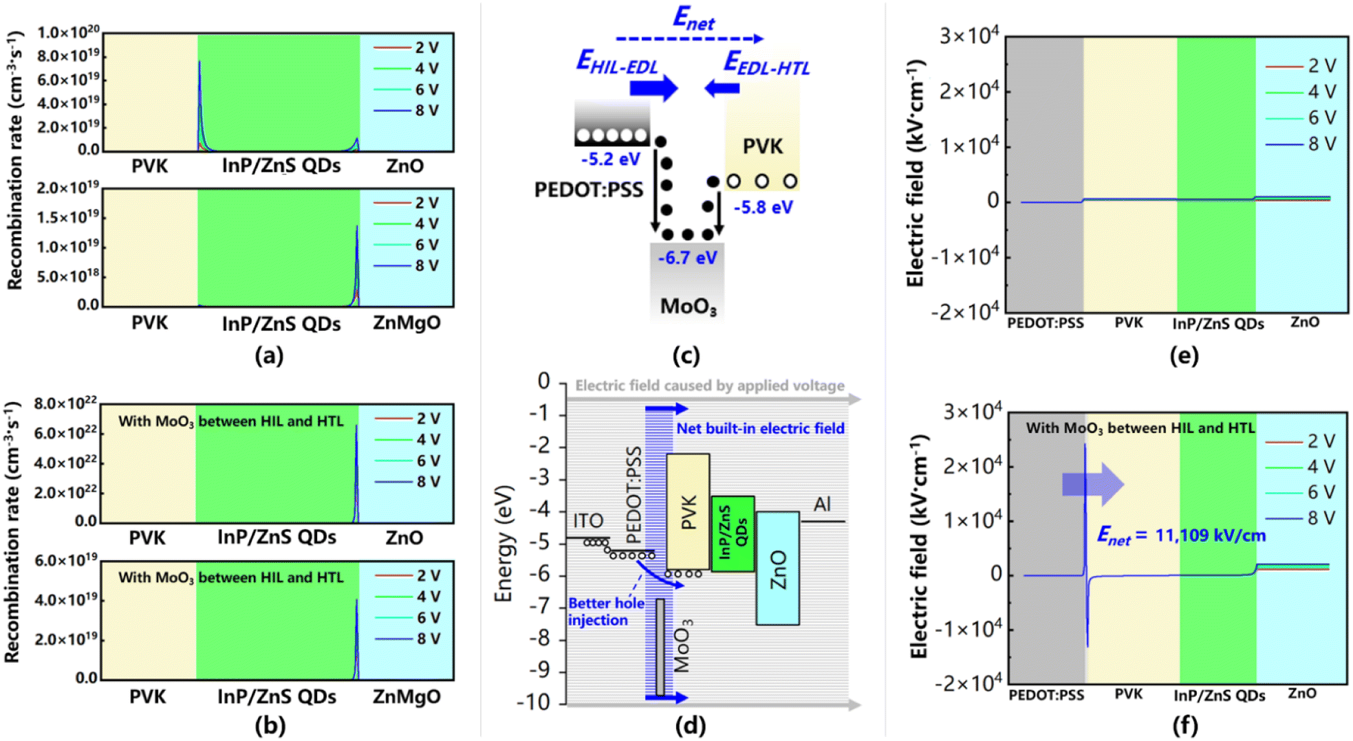 | ||
| Fig. 1 (a) Distribution of the recombination rate in the green InP QLED without MoO3. (b) Distribution of the recombination rate in the green InP QLED with MoO3. (c) Schematic of carrier transfer in the PEDOT:PSS/MoO3/PVK structure. (d) Schematic of hole transfer at PEDOT:PSS/MoO3/PVK interfaces in the green InP QLED. (e) Simulation of the distribution of the electric field in the PEDOT:PSS/PVK/ZnO structure. (f) Simulation of the distribution of the electric field in the PEDOT:PSS/MoO3/PVK/ZnO structure. | ||
Materials
PEDOT:PSS (Clevios™ P VP Al 4083) was purchased from Xi'an p-OLED Ltd. and used directly without any further dilution. PVK was purchased from Lumtec Ltd. and dissolved in chlorobenzene as 8 mg mL−1. Green InP/ZnS QDs were purchased from Fullnano Ltd. and dissolved in octane at 10 mg mL−1. The diameter of green InP/ZnS QDs was 4.8 ± 0.2 nm and the ligands were TOP/OA. ZnMgO NPs (suspended in ethanol, 20 mg mL−1) and ZnO NPs (suspended in ethanol, 20 mg mL−1) were purchased from Mesolight Ltd. MoO3 was purchased from Xi'an p-OLED Ltd.Device fabrication
The QLED devices were fabricated with a structure of ITO/poly(3,4-ethylenedioxythiophene):poly(styrenesulfonate) (PEDOT:PSS, 25 nm)/poly(9-vinylcarbazole) (PVK, 30 nm)/QDs (25 nm)/ZnMgO (30 nm) or ZnO (30 nm)/Al. The electron-only devices (EODs) were fabricated with a structure of ITO/QDs (25 nm)/Zn(Mg)O (30 nm)/Al. The hole-only devices (HODs) were fabricated with a structure of ITO/PEDOT:PSS (25 nm)/MoO3 (0 or 0.3 nm)/PVK (30 nm)/QDs (25 nm)/Al. The patterned ITO electrodes were cleaned and treated with plasma before use. All the functional layers except MoO3 were deposited via spin-coating at 3000 rpm for 45 s with the assistance of thermal annealing. MoO3 (0.1 nm, 0.3 nm, 0.5 nm and 0.7 nm) and Al electrodes (100 nm) were deposited by thermal evaporation at an average rate of 0.01 and 0.2 nm s−1 respectively under a vacuum of 5 × 10⁻⁴ Pa.Characterization
The energy levels of green InP/ZnS QDs used in simulations were measured in a film form by ultraviolet photoelectron spectroscopy (UPS). The luminance area of our devices was 2 mm × 2 mm. The PLQY and PL spectra were recorded with an excitation wavelength of 365 nm by using an absolute PLQY spectrometer (Hamamatsu Quantaurus QY C11347-12). The devices were considered as a Lambert illuminant, and the current density–voltage–luminance (J–V–L) curves were recorded by using a Keithley 2614B source and a PIN-25D silicon photodiode. The capacitance–voltage (C–V) curves were recorded by using a LCR meter (Agilent 4284A). All measurements were performed at room temperature.Results and discussion
We have established carrier recombination models according to actual green InP QLEDs. The core and shell of green InP/ZnS QDs were simulated together as a whole material in the simulations to ensure the accuracy of the simulation under the permission of software computing power.42–44 The energy level data of the green InP QDs used in this work are measured by UPS (Fig. S1†). Fig. 1a shows the distribution of the recombination rate at different bias voltages (2 V, 4 V, 6 V and 8 V) in the green InP QLEDs based on two different ETLs (ZnO and ZnMgO). There are two obvious peaks in the ZnO-based device and the stronger one located near the PVK/QD interface has a recombination rate of 7.66 × 1019 cm−3 s−1. This recombination peak is higher than that in the ZnMgO-based device (1.37 × 1019 cm−3 s−1). Here, ZnMgO has suppressed the injection of electrons due to its low electron mobility (4.5 × 10⁻⁴ cm2 V−1 s−1). The lower electron injection rate is better matched with the poor hole injection in InP QLEDs. However, inhibiting the carrier injection has limited the potential of a higher recombination rate in green InP QLEDs. In addition, applying ZnMgO as the ETL will confine the electron injection but the energy barrier between the HIL and HTL still exists. In these green InP QLEDs, the HIL is PEDOT:PSS (HOMO = −5.2 eV) and the HTL is PVK (HOMO = −5.8 eV), which means that there is a 0.6 eV barrier at their interface. As it is hard to inject holes from PEDOT:PSS to PVK, the problem of hole accumulation at the HIL/HTL interface is still unsolved. To enhance hole injection and achieve a higher recombination rate at the same time, an ultra-thin MoO3 layer is inserted at the interface of PEDOT:PSS and PVK. As shown in Fig. 1b, the recombination peak located near the PVK/QD interface disappears in the ZnO-based device and the major recombination peak is located near the QDs/ZnO interface with a peak rate of 6.58 × 1022 cm−3 s−1, which is three orders of magnitude larger than that of 7.66 × 1019 cm−3 s−1 without the MoO3 layer. Meanwhile, the recombination peak of the ZnMgO-based device is also improved to 4.07 × 1019 cm−3 s−1, enhancement of which is not as large as that of the ZnO-based device due to the much lower electron mobility of ZnMgO compared with ZnO.The simulation result illustrates that the insertion of the MoO3 layer has strengthened the hole injection in green InP QLEDs, and hence the major recombination center shifts toward the QDs/ZnO interface and the recombination rate enhanced dramatically. Indeed, the MoO3 layer has acted as an electric dipole layer (EDL) here.45 Electrons tend to diffuse from PEDOT:PSS and PVK to the deep-lying conduction band of MoO3 (−6.7 eV), leaving holes in PEDOT:PSS and PVK (Fig. 1c). The remnant holes in PEDOT:PSS and PVK along with the excess electrons in MoO3 will generate pairs of dipoles that form two built-in electric fields (EHIT-EDL and EEDL-HTL). Owing to the larger energy level difference between PEDOT:PSS and MoO3 (1.5 eV) compared with that of MoO3 and PVK (0.9 eV), the positive built-in electric field EHIL-EDL is larger than the negative EEDL-HTL. Thus, the net electric field (Enet) is in the same direction of the electric field driven by the applied forward voltage as shown in Fig. 1d. Therefore, the hole injection from PEDOT:PSS to PVK has been strengthen by Enet. The above explanation has been further confirmed by simulation. Different from the case without MoO3 (Fig. 1e), the magnitude of the positive electric field in the MoO3-based device is higher than that of the negative electric field by 11109 kV cm−1 (Fig. 1f). Therefore, a positive electric field is dominant in the hole hopping process. Due to the shift of the recombination center, the electron concentration difference at the QDs/ZnO interface makes electrons diffuse from ZnO to the QD layer and form a built-in electric field. As shown in Fig. 1f, this process will finally reach a dynamic equilibrium and make the electric field at the QDs/ZnO interface higher than that in Fig. 1e. Overall, the MoO3 introduced in the simulations can successfully generate electric dipoles and a strong built-in electric field at the interface between the HIL and HTL, and hence a higher recombination rate is achieved in green InP QLEDs.
Fig. 2a shows the current density versus voltage of the electron-only device (EOD). Apparently, in comparison to that of the ZnMgO-based device, the EOD with ZnO effectively enhance the ability of electron injection. It confirms once again that the higher electron mobility of ZnO will achieve a better electron injection. Meanwhile, as mentioned earlier, the MoO3 EDL helps the hole hopping due to the built-in electric field. As a result, the current density versus voltage of the hole-only device (HOD) reveals a remarkable enhancement of the hole injection ability for the MoO3 EDL modified device (Fig. 2b). When the applied voltage is lower than 1 V, MoO3 shows a slightly negative impact on the current injection in the HOD. This phenomenon could be attributed to the trap-filling effect with the introduction of MoO3 from the analysis based on the space charge limited current (SCLC) model.46–48 As these single carrier devices are fabricated with the structures of half QLED device,25 the current density of EODs and HODs can be used to estimate the electron injection and hole injection in a complete QLED respectively. Furthermore, these current densities can be used for comparison at a same voltage. Evidently, after ETL and EDL modification, the higher electron mobility and the hole hopping enable more balance between electron and hole injection. It will enhance the radiation recombination rate in the QD layer, resulting in highly efficient green InP QLEDs.
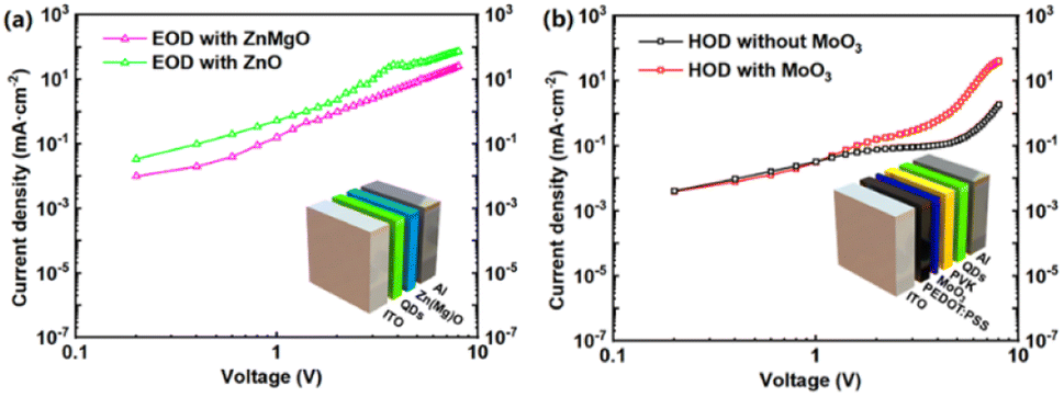 | ||
| Fig. 2 Characterization of single-carrier devices. The current density–voltage profiles of the (a) electron-only devices with ZnO or ZnMgO, and (b) hole-only devices with/without the MoO3 layer. The inserts show the schematic diagram of electron and hole-only device structures. | ||
To further verify the effect of ETL and EDL modification in simulation results, green InP QLEDs were fabricated with the green InP/ZnS QDs and characterized to demonstrate the enhancement of carrier injection. The purchased green InP/ZnS QDs have an average size of 4.8 ± 0.2 nm and their ligands are TOP/OA (Fig. 3a). The typical device structure with the MoO3 layer is shown in Fig. 3b, and a device without the MoO3 layer is fabricated for comparison. Meanwhile, the ETL is replaced by ZnMgO in two other comparison devices. Fig. 3c shows the electroluminescence (EL) spectra of the proposed QLEDs and there is a negligible shift (<1 nm) between these devices. Compared with the PL spectra of green InP/ZnS QD solution (Fig. S2†), there is a red-shift for EL from 525 to 535 nm due to the quantum-confined Stark effect. The inset graph exhibits the pure and bright-light green emission of the InP QLED device at 5 V bias. The current density–voltage–luminance (J–V–L) characteristics are shown in Fig. 3d. The green InP QLEDs with the ZnO ETL exhibits higher current density (82.23 mA cm−2 @ 5 V) than the ZnMgO-based device (63.25 mA cm−2 @ 5 V). It indicates that electron injection has been significantly enhanced due to the higher electron mobility of ZnO. Benefiting from the hole injection strengthened by the positive built-in electric field, the current density is further promoted to 142.30 mA cm−2 @ 5 V after the insertion of the MoO3 layer (red color curve with solid dots in Fig. 3d). The simultaneous enhancements of electron and hole injection promotes the recombination rate. As a consequence, the maximum luminance of the green InP QLED is enhanced from 6482 to 6794 (applying a ZnO ETL) and then to 52730 cd m−2 (inserting a MoO3 interlayer), which is an 8.1 times improvement overall. As demonstrated in Fig. 3e, the EQE of the ZnO-based green InP QLEDs increased from 4.25% to 7.39% and the ZnMgO-based one increased from 4.69% to 6.19%. The low EQE of the ZnO-based contrast device indicates that the excess electron injection leads more non-radiative recombination. However, the larger EQE enhancement of the ZnO-based device confirms that a higher recombination rate and good carrier balance have been achieved by the ZnO ETL and MoO3 interlayer. The enhancement of carrier injection improves the current density of the devices (inset image in Fig. 3d), which may lead to a short lifetime of the devices. Nevertheless, the damage of accumulated holes at the PEDOT:PSS/PVK interface was reduced more obviously because the hole hopping was enhanced by the EDL. As a result, the phenomenon of efficiency roll-off had been finally relieved by the MoO3 interlayer. The ZnO-based green InP QLED with the MoO3 EDL exhibited a longer lifetime, and its T50 at 100 cd m−2 is predicted to be 104.09 h, using an acceleration factor of 1.8 (given that we measured the real lifetime at 1000 cd m−2), compared to the device without the EDL (T50 = 15.77 h) (Fig. 3f). Furthermore, the T50 at 100 cd m−2 of the ZnMgO-based green InP QLED with the MoO3 EDL is predicted to be 280.75 h (Table S2†). The longer lifetime is mainly due to the higher EQE and carrier recombination rate of the ZnMgO-based device with the EDL under a luminance of 1000 cd m−2, so it will suffer from less damage from accumulated carriers.
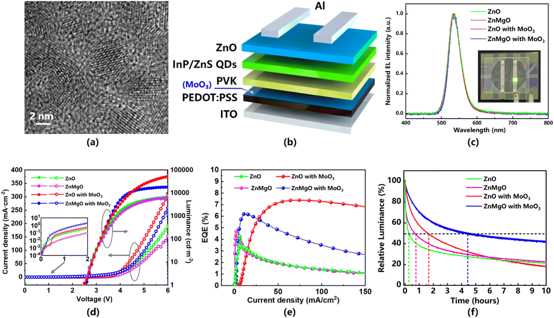 | ||
| Fig. 3 (a) A TEM image of the purchased green InP/ZnS QDs with an average size of 4.8 ± 0.2 nm. (b) The device structure of typical green InP QLEDs with the MoO3 interlayer. (c) EL spectra under the same measuring conditions (5 V). Inset: photographs of the operating device. (d) J–V–L characteristics. Inset: J–V characteristics on a log scale in the low-voltage region, (e) EQE versus J and (f) lifetime with an initial luminance of 1000 cd m−2 of the green InP QLEDs with different ETLs (ZnMgO and ZnO) and with/without the MoO3 interlayer. | ||
In order to better understand the role of the ultra-thin MoO3 interlayer in the improvement of device performance, MoO3 layers with different thicknesses were compared in this work (Fig. 4a). Since the ultra-thin interlayer may not form as a dense film, we evaluated them here using the average thickness (0.1 nm, 0.3 nm, 0.5 nm and 0.7 nm), which can be metered by the crystal oscillator of the evaporation equipment. Different thicknesses of the films can be achieved by controlling the evaporation rate and time (Table S3†). When the average thickness of the MoO3 layer was less than 0.3 nm, the thickness of the film is even smaller than the diameter of a molecule. Therefore, the 0.1 nm average thickness measured by the crystal oscillator can be considered that there was only a small amount of MoO3 molecular deposition. Similarly, although 0.3 nm MoO3 performed best here, it only represented the average thickness value of an incomplete film. When the thickness of MoO3 increased, it would suppress the hole hopping due to the long minimal hopping distance. The low-frequency C–V results of green InP QLEDs with different average thickness MoO3 layers presented a very different tendency than that of the device without the MoO3 interface layer (Fig. 4b). The capacitance values remained nearly constant under 2 V, which suggested that charge injection had not yet been initiated at this low bias voltage. When the voltage was increased from 2 V, the capacitance of the green InP QLED without the MoO3 layer increased significantly. In this process, more and more carriers were injected in this device with the increase of applied voltage, and only some of them underwent radiation recombination. When the applied voltage was 4.3 V, there was a capacitance peak for the contrast device without MoO3 (black color curve). After this capacitance peak, the recombination rate of carriers would be higher than that of accumulation and their growth difference would lead to steeper decreases in capacitance. However, there was almost no obvious rising region in the curves of green InP QLEDs with MoO3, which meant that carriers were nearly not hindered during the injection process. The recombination peak appeared earliest on the curve of 0.3 nm MoO3 and its appearance gradually delayed with the increase of the average thickness (0.5 and 0.7 nm). It confirmed that the increase of the thickness would suppress the hole hopping. There were some fluctuations on the C–V curve of InP QLEDs, which may be caused by the oxidative damaged QD film. The oxidized InP/ZnS QDs with irregular shapes will lead to a poor contact at the interface. When current is injected into a InP QLED, local high current density due to the unideal contact may lead to some local damage to the interface, which will release the accumulated carriers and result in some sudden drops as shown in the curve. As the accumulation speed of carriers under high voltage is much higher than the amount of temporary release, the capacitance curve will return to the original upward trend. The sudden release of carriers and the subsequent carrier accumulation will be reflected as a fluctuation in the C–V curve.
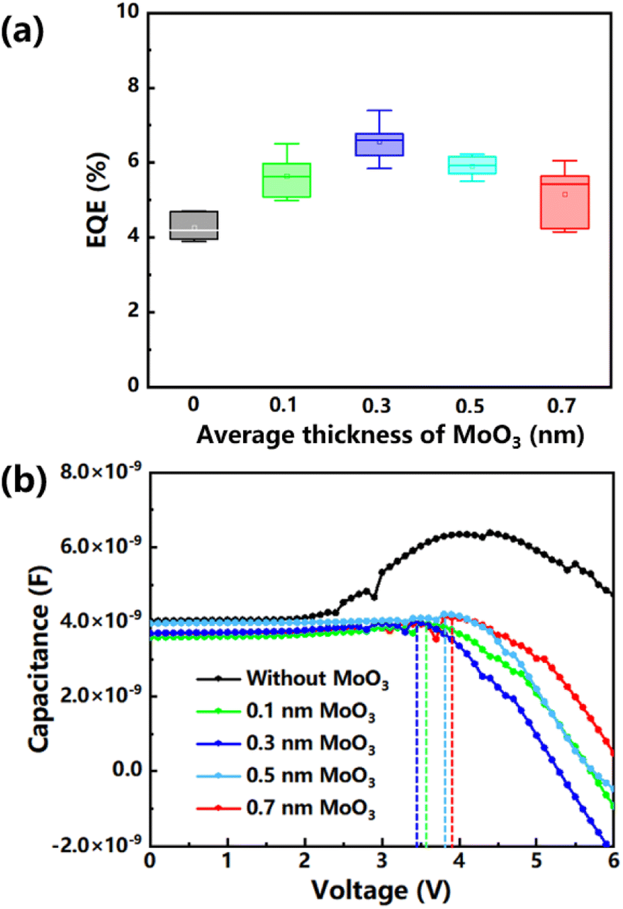 | ||
| Fig. 4 (a) The reproducibility of the maximum of EQE (6 samples for each group) and (b) C–V results of green InP QLED devices for green InP QLED devices with different average thickness MoO3 interlayers (0, 0.1 nm, 0.3 nm, 0.5 nm and 0.7 nm). | ||
To further confirm the film formation of MoO3, we have examined the MoO3 on the ITO/PEDOT:PSS surface using an energy dispersive spectrometer (EDS) and an atomic force microscope (AFM). Fig. 5a–e and f–j show the EDS compositional mapping images and AFM images for ITO/PEDOT:PSS with different MoO3 layer thicknesses of 0, 0.1 nm, 0.3 nm, 0.5 nm and 0.7 nm respectively. The increasing trend of element Mo in the mapping confirmed the existence of MoO3. It can be found that the film in Fig. 5j is relatively uniform and little thicker compared with the bare ITO/PEDOT:PSS sample in Fig. 5f. Nevertheless, it is difficult to prove the effect of the rare and unevenly distributed MoO3 in Fig. 5a–e. For further assessment, MoO3 is deposited on the ITO substrates and their EDS compositional mapping images are shown in Fig. 5k–o. On this inorganic and dense substrate, the same amount of MoO3 shows more proportion. Once the thickness of the MoO3 layer increases to 2 nm, the Mo element is dense and uniformly dispersed (Fig. S3†). Under this circumstance, the MoO3 layer deposited on the ITO/PEDOT:PSS substrate is most likely MoO3 molecules embedded in the PEDOT:PSS film.
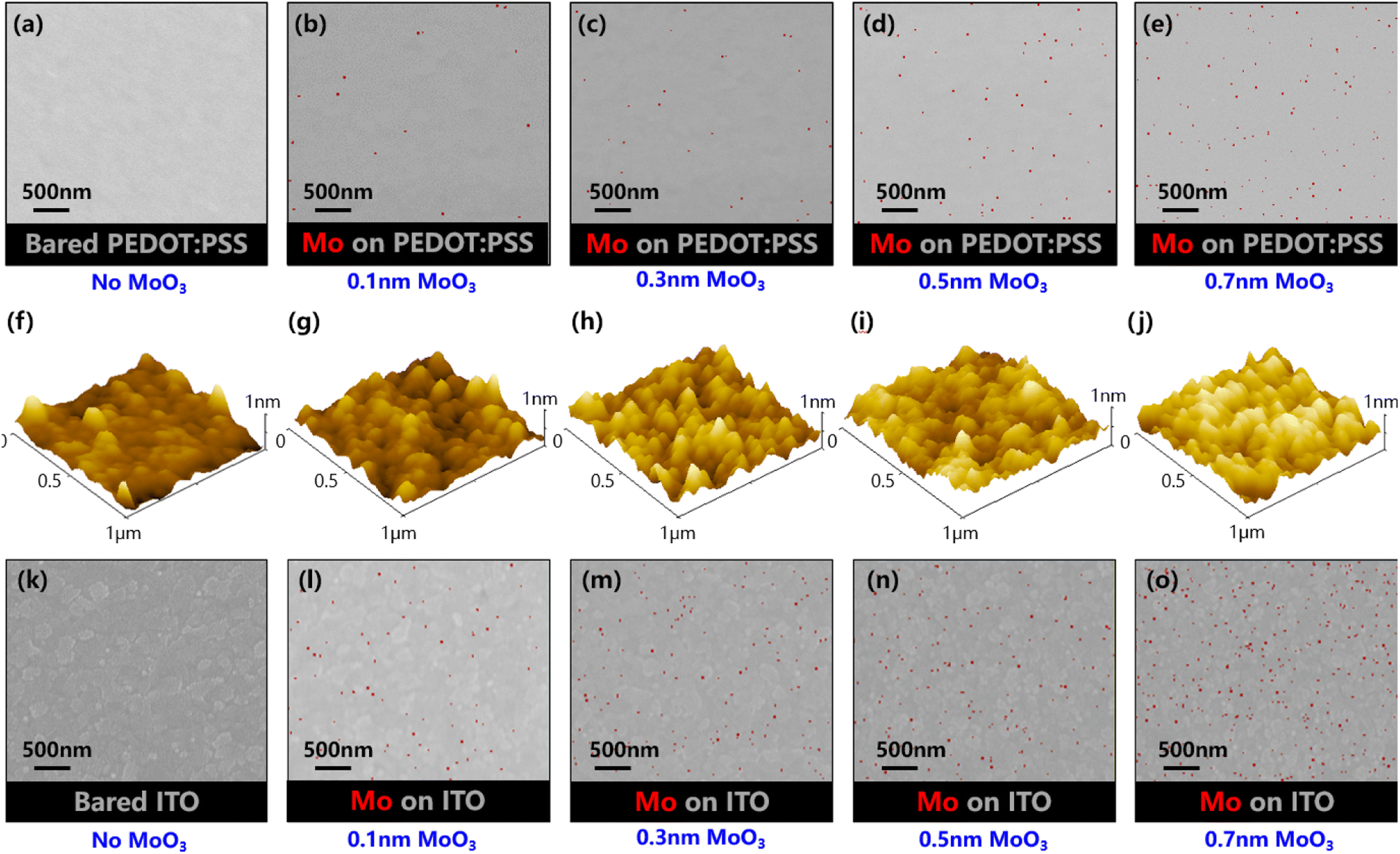 | ||
| Fig. 5 EDS compositional mapping images (top view) for ITO/PEDPT:PSS (a)–(e) and ITO (k)–(o) modified with different average thicknesses of the MoO3 layer, (a) and (f) no MoO3, (b) and (g) 0.1 nm, (c) and (h) 0.3 nm, (d) and (i) 0.5 nm and (e) and (j) 0.7 nm. AFM images of the corresponding samples on ITO/PEDOT:PSS are shown in (f)–(j). | ||
Fig. 6 shows the working mechanism of embedded MoO3. Initially, MoO3 is embedded in the PEDOT:PSS film while electrons are contained in PEDOT:PSS and PVK layers (Fig. 6a). Due to the deep-lying CB of MoO3, electrons tend to diffuse into it from PEDOT:PSS and PVK. While the electrons are leaving, related holes are left at the interfaces (Fig. 6b). Then, electrons in adjacent areas will continually diffuse to the interface due to the concentration difference. This process in Fig. 6c will continue until the electron concentration at the interface reaches a dynamic equilibrium under a built-in electric field. During the whole process, electron and hole pairs will be formed as electric dipoles at the interface. Such a result as shown in Fig. 6c can be considered a more microscopic illustration of Fig. 1c. Therefore, the role of the MoO3 interlayer in these devices could also be considered as a modification of the interface between the HIL and HTL. The small amount of MoO3 with an ultra-thin average thickness still realize a good performance in electron collection. Although it was not a dense film, electric dipoles could also form a strong enough electric field to enhance hole hopping and reduce the energy barrier at the PEDOT:PSS/PVK interface sufficiently.
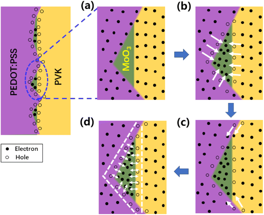 | ||
| Fig. 6 Schematic of the carrier transfer in the interface region where MoO3 is embedded in. | ||
Conclusions
In summary, we have introduced a MoO3 electric dipole layer to enhance hole injection in green InP QLEDs with a ZnO ETL. This approach can effectively improve the recombination rate in green InP QLEDs and achieve highly efficient devices. By simulations and experiments, we demonstrated that the green InP QLED with ZnO as the ETL had a higher recombination rate than the ZnMgO-based device due to the high electron mobility of ZnO. As a solution, an ultra-thin MoO3 electric dipole layer was introduced to enhance the hole injection. The MoO3 interface layer would form a positive built-in electric field at the HIL/HTL interface due to its deep conduction band level. A strong built-in electric field is produced for efficient hole hopping, and the carrier recombination rate is substantially increased. Benefiting from the high electron mobility of the ZnO ETL and the enhancement of hole injection, a green InP QLED with an optimized 0.3 nm average thickness MoO3 interlayer had achieved a high luminance of 52730 cd m−2 and an improved EQE of 7.39%, indicating a feasible approach to promote the green InP QLED performance.
Author contributions
Tianqi Zhang: conceptualization, investigation, and writing – original draft. Pai Liu: investigation, methodology and formal analysis. Fangqing Zhao: investigation and validation. Yangzhi Tan: methodology and validation. Jiayun Sun: investigation and validation. Xiangtian Xiao: formal analysis and methodology. Zhaojing Wang: investigation and data curation. Qingqian Wang: investigation and validation. Fankai Zheng: methodology and formal analysis. Xiao Wei Sun: methodology, resources and supervision. Dan Wu: resources and supervision. Guichuan Xing: supervision, resources, funding acquisition and writing – review & editing. Kai Wang: conceptualization, formal analysis, project administration, resources, writing – review & editing and funding acquisition.Conflicts of interest
There are no conflicts to declare.Acknowledgements
This work was supported by the National Key Research and Development Program (No. 2019YFB1704600), National Natural Science Foundation of China (No. 61875082, No. 61905107 and No. 62122034), Key-Area Research and Development Program of Guangdong Province (No. 2019B010924001), Guangdong University Key Laboratory for Advanced Quantum Dot Displays and Lighting (No. 2017KSYS007), Innovation Project of Department of Education of Guangdong Province (No. 2019KTSCX157) and Shenzhen Innovation Project (No. JCYJ20190809152411655 and No. JCYJ20210324104413036). G. X. acknowledges the Science and Technology Development Fund, Macao SAR (File no. FDCT-0044/2020/A1, 0082/2021/A2), UM's research fund (File no. MYRG2020-00151-IAPME), Natural Science Foundation of China (61935017, 62175268), Guangdong-Hong Kong-Macao Joint Laboratory of Optoelectronic and Magnetic Functional Materials (2019B121205002), and Shenzhen-Hong Kong-Macao Science and Technology Innovation Project (Category C) (SGDX2020110309360100).References
- V. L. Colvin, M. C. Schlamp and A. P. Alivisatos, Nature, 1994, 370, 354–357 CrossRef CAS.
- X. L. Dai, Z. X. Zhang, Y. Z. Jin, Y. Niu, H. J. Cao, X. Y. Liang, L. W. Chen, J. P. Wang and X. G. Peng, Nature, 2014, 515, 96–99 CrossRef CAS.
- J. J. Hao, H. C. Liu, J. Miao, R. Lu, Z. M. Zhou, B. X. Zhao, B. Xie, J. J. Cheng, K. Wang and M. H. Delville, Sci. Rep., 2019, 9, 12048 CrossRef.
- W. R. Cao, C. Y. Xiang, Y. X. Yang, Q. Chen, L. W. Chen, X. L. Yan and L. Qian, Nat. Commun., 2018, 9, 2608 CrossRef PubMed.
- J. H. Jo, J. H. Kim, S. H. Lee, H. S. Jang, D. S. Jang, J. C. Lee, K. U. Park, Y. Y. Choi, C. H. Ha and H. Yang, J. Alloys Compd., 2015, 647, 6–13 CrossRef CAS.
- H. C. Liu, H. Y. Zhong, F. K. Zheng, Y. Xie, D. P. Li, D. Wu, Z. M. Zhou, X.-W. Sun and K. Wang, Chin. Phys. B, 2019, 28, 128504 CrossRef CAS.
- J. Z. Song, J. H. Li, X. M. Li, L. M. Xu, Y. H. Dong and H. B. Zeng, Adv. Mater., 2015, 27, 7162–7167 CrossRef CAS.
- X. M. Li, Y. Wu, S. L. Zhang, B. Cai, Y. Gu, J. Z. Song and H. B. Zeng, Adv. Funct. Mater., 2016, 26, 2435–2445 CrossRef CAS.
- Z. C. Li, Z. M. Chen, Y. C. Yang, Q. F. Xue, H. L. Yip and Y. Cao, Nat. Commun., 2019, 10, 1027 CrossRef.
- L. N. Kolonel, Cancer, 1976, 37, 1782–1787 CrossRef CAS.
- L. Järup, Br. Med. Bull., 2003, 68, 167–182 CrossRef.
- A. A. Guzelian, J. E. B. Katari, A. V. Kadavanich, U. Banin, K. Hamad, E. Juban, A. P. Alivisatos, R. H. Wolters, C. C. Arnold and J. R. Heath, J. Phys. Chem., 1996, 100, 7212–7219 CrossRef CAS.
- O. I. Mićić, H. M. Cheong, H. Fu, A. Zunger, J. R. Sprague, A. Mascarenhas and A. J. Nozik, J. Phys. Chem. B, 1997, 101, 4904–4912 CrossRef.
- A. Q. Wang, H. B. Shen, S. P. Zang, Q. L. Lin, H. Z. Wang, L. Qian, J. Z. Niu and L. S. Li, Nanoscale, 2015, 7, 2951–2959 RSC.
- C. Y. Xiang, W. Koo, S. Chen, F. So, X. Liu, X. X. Kong and Y. J. Wang, Appl. Phys. Lett., 2012, 101, 5 Search PubMed.
- X. Huang, R. M. Yu, X. Q. Yang, X. M. Xu, H. Zhang and D. D. Zhang, Efficient CuInS2/ZnS based quantum dot light emitting diodes by engineering the exciton formation interface, J. Lumin., 2018, 202, 339–344 CrossRef CAS.
- L. Li, A. Pandey, D. J. Werder, B. P. Khanal, J. M. Pietryga and V. I. Klimov, J. Am. Chem. Soc., 2011, 133, 1176–1179 CrossRef CAS.
- F. Wang, Y. H. Chen, C. Y. Liu and D. G. Ma, Chem. Commun., 2011, 47, 3502–3504 RSC.
- B. H. Kim, C. H. Cho, J. S. Mun, M. K. Kwon, T. Y. Park, J. S. Kim, C. C. Byeon, J. M. Lee and S. J. Park, Adv. Mater., 2008, 20, 3100–3104 CrossRef CAS.
- P. Liu, Y. J. Lou, S. H. Ding, W. D. Zhang, Z. H. Wu, H. C. Yang, B. Xu, K. Wang and X. W. Sun, Adv. Funct. Mater., 2021, 31, 11 Search PubMed.
- D. Battaglia and X. G. Peng, Nano Lett., 2002, 2, 1027–1030 CrossRef CAS.
- L. Li and P. Reiss, J. Am. Chem. Soc., 2008, 130, 11588–11589 CrossRef CAS PubMed.
- H. Moon, W. Lee, J. Kim, D. Lee, S. Cha, S. Shin and H. Chae, Chem. Commun., 2019, 55, 13299–13302 RSC.
- S. H. Guo, Q. Q. Wu, L. Wang, F. Cao, Y. J. Dou, Y. M. Wang, Z. J. Sun, C. X. Zhang and X. Y. Yang, IEEE Electron Device Lett., 2021, 42, 1806–1809 CAS.
- W. C. Chao, T. H. Chiang, Y. C. Liu, Z. X. Huang, C. C. Liao, C. H. Chu, C. H. Wang, H. W. Tseng, W. Y. Hung and P. T. Chou, Commun. Mater., 2021, 2, 1 CrossRef.
- Q. Su, H. Zhang and S. M. Chen, Appl. Phys. Lett., 2020, 117 Search PubMed.
- B. S. Mashford, M. Stevenson, Z. Popovic, C. Hamilton, Z. Q. Zhou, C. Breen, J. Steckel, V. Bulovic, M. Bawendi, S. Coe-Sullivan and P. T. Kazlas, Nat. Photonics, 2013, 7, 407–412 CrossRef CAS.
- Y. X. Yang, Y. Zheng, W. R. Cao, A. Titov, J. Hyvonen, J. R. Manders, J. Xue, P. H. Holloway and L. Qian, Nat. Photonics, 2015, 9, 259–266 CrossRef CAS.
- H. Zhang, N. Hu, Z. P. Zeng, Q. L. Lin, F. J. Zhang, A. W. Tang, Y. Jia, L. S. Li, H. B. Shen, F. Teng and Z. L. Du, Adv. Opt. Mater., 2019, 7, 7 Search PubMed.
- M. H. Lee, W. H. Choi and F. Zhu, Opt. Express, 2016, 24, A592 CrossRef CAS.
- Y. Kwon, Y. Kim, H. Lee, C. Lee and J. Kwak, Org. Electron., 2014, 15, 1083 CrossRef CAS.
- M. H. Lee, L. X. Chen, N. Li and F. Zhu, J. Mater. Chem. C, 2017, 5, 10555 RSC.
- H. J. Wang, Z. G. Liu, Q. M. Dong, D. Zhang and R. Han, 19th International Conference on Optical Communications and Networks (ICOCN), 2021 Search PubMed.
- L. Z. Zhu, B. J. Richardson and Q. M. Yu, Phys. Chem. Chem. Phys., 2016, 18, 3463 RSC.
- X. Y. Li, Q. L. Lin, J. J. Song, H. B. Shen, H. M. Zhang, L. S. Li, X. G. Li and Z. L. Du, Adv. Opt. Mater., 2020, 8(2), 2020 Search PubMed.
- Z. H. Wu, P. Liu, W. D. Zhang, K. Wang and X. W. Sun, ACS Energy Lett., 2020, 5, 1095–1106 CrossRef CAS.
- H. C. Wang, H. Zhang, H. Y. Chen, H. C. Yeh, M. R. Tseng, R. J. Chung, S. M. Chen and R. S. Liu, Small, 2017, 13, 1603962 CrossRef.
- T. Lee, D. Hahm, K. Kim, W. K. Bae, C. Lee and J. Kwak, Small, 2019, 15, 1905162 CrossRef CAS.
- D. Hahm, J. H. Chang, B. G. Jeong, P. Park, J. Kim, S. Lee, J. Choi, W. D. Kim, S. Rhee, J. Lim, D. C. Lee, C. Lee, K. Char and W. K. Bae, Chem. Mater., 2019, 31, 3476–3484 CrossRef CAS.
- G. Motomura, K. Ogura, Y. Iwasaki, J. Nagakubo, M. Hirakawa, T. Nishihashi and T. Tsuzuki, AIP Adv., 2020, 10, 6 Search PubMed.
- Y. Iwasaki, G. Motomura, K. Ogura and T. Tsuzuki, Appl. Phys. Lett., 2020, 117, 11 CrossRef.
- Q. L Yuan, T. Wang, R. Wang, J. L. Zhao, H. Z Zhang and W. Y. Ji, Opt. Lett., 2020, 45, 6370 CrossRef.
- S. H. Lv, K. Y. Yang, C. X. Wu, K. Wang, R. Chen, X. Chen, S. M Ju, Z. Q. Luo, H. B. Zhao, T. L. Guo and F. S. Li, IEEE Electron Device Lett., 2022, 43, 256 CAS.
- Z. Wang, W. D. Sun, P. Liu, Z. B. Wang, J. Zhang, J. L. Wei, Y. Li, T. Hayat, A. Alsaedi and Z. A. Tan, J. Phys. Chem. Lett., 2019, 10, 960 CrossRef.
- X. T. Xiao, K. Wang, T. K. Ye, R. Cai, Z. W. Ren, D. Wu, X. W. Qu, J. Y. Sun, S. H. Ding, X. W. Sun and W. C. H. Choy, Commun. Mater., 2020, 1, 1 CrossRef.
- P. Mark and W. Helfrich, J. Appl. Phys., 1962, 33, 205–215 CrossRef CAS.
- M. A. Lampert, Phys. Rev., 1956, 103, 1648–1656 CrossRef CAS.
- S. K. Kim and Y. S. Kim, J. Appl. Phys., 2019, 126, 3 Search PubMed.
Footnote |
| † Electronic supplementary information (ESI) available. See DOI: https://doi.org/10.1039/d2na00705c |
| This journal is © The Royal Society of Chemistry 2023 |