
 Open Access Article
 This Open Access Article is licensed under a
 Creative Commons Attribution 3.0 Unported Licence
Discovery of a metastable van der Waals semiconductor via polymorphic crystallization of an amorphous film†
Yuta
Saito
 *a,
Shogo
Hatayama
a,
Wen Hsin
Chang
a,
Naoya
Okada
a,
Toshifumi
Irisawa
a,
Fumihiko
Uesugi
b,
Masaki
Takeguchi
b,
Yuji
Sutou
cd and
Paul
Fons
ae
*a,
Shogo
Hatayama
a,
Wen Hsin
Chang
a,
Naoya
Okada
a,
Toshifumi
Irisawa
a,
Fumihiko
Uesugi
b,
Masaki
Takeguchi
b,
Yuji
Sutou
cd and
Paul
Fons
ae
aDevice Technology Research Institute, National Institute of Advanced Industrial Science and Technology (AIST), Tsukuba Central 2, 1-1-1 Umezono, Tsukuba, 305-8568, Japan. E-mail: yuta-saito@aist.go.jp
bElectron Microscopy Analysis Station, National Institute for Materials Science (NIMS), 1-2-1 Sengen, Tsukuba, 305-0047, Japan
cDepartment of Materials Science, Graduate School of Engineering, Tohoku University, 6-6-11 Aoba-yama, Sendai, 980-8579, Japan
dAdvanced Institute for Materials Research (AIMR), Tohoku University, 2-1-1 Katahira, Sendai, 980-8577, Japan
eDepartment of Electronics and Electrical Engineering, Faculty of Science and Technology, Keio University, 3-14-1 Hiyoshi, Kohoku-ku, Yokohama, 223-8522, Japan
First published on 6th April 2023
Abstract
Here we report on the growth of thin crystalline films of the metastable phase GeTe2. Direct observation by transmission electron microscopy revealed a Te–Ge–Te stacking with van der Waals gaps. Moreover, electrical and optical measurements revealed the films exhibted semiconducting properties commensurate with electronics applications. Feasibility studies in which device structures were fabricated demonstrated the potential application of GeTe2 as an electronic material.
New conceptsIn this paper, the concept of “metastable” layered materials has been proposed, and the fabrication of metastable van der Waals GeTe2 was demonstrated. The growth process proceeds via the amorphous phase, where an initial amorphous film is sputter-deposited and then undergoes a carefully controlled thermal annealing process resulting in the formation of the metastable crystalline phase. The choice of the initial composition Ge![[thin space (1/6-em)]](https://www.rsc.org/images/entities/char_2009.gif) :Te = 1:2 enabled the formation of a Te–Ge–Te three-layer unit. In general, studies of van der Waals materials can be categorized into two regimes: exfoliation from a bulk single crystal, and growth by chemical vapor deposition using gas sources. The former method inevitably requires bulk material, which is typically the equilibrium phase, while the latter involves direct fabrication of a stable crystalline phase under nearly thermodynamically equilibrium conditions. Our concept is strikingly different from the aforementioned methods in that the fabrication of the metastable van der Waals phase is achieved directly via solid-state crystallization. Intriguingly, the fabricated GeTe2 film was found to exhibit semiconducting properties. This work introduces a conceptually new fabrication method for metastable van der Waals materials and will open the door to the exploration of novel materials that could unlock great potential for future electronics beyond contemporary Si technology. :Te = 1:2 enabled the formation of a Te–Ge–Te three-layer unit. In general, studies of van der Waals materials can be categorized into two regimes: exfoliation from a bulk single crystal, and growth by chemical vapor deposition using gas sources. The former method inevitably requires bulk material, which is typically the equilibrium phase, while the latter involves direct fabrication of a stable crystalline phase under nearly thermodynamically equilibrium conditions. Our concept is strikingly different from the aforementioned methods in that the fabrication of the metastable van der Waals phase is achieved directly via solid-state crystallization. Intriguingly, the fabricated GeTe2 film was found to exhibit semiconducting properties. This work introduces a conceptually new fabrication method for metastable van der Waals materials and will open the door to the exploration of novel materials that could unlock great potential for future electronics beyond contemporary Si technology.
|
Introduction
Layered materials are of great interest in fundamental and applied physics, chemistry, and materials sciences. 2D or van der Waals (vdW) materials, representing the monolayer limit of layered materials, can be formed through exfoliation from a bulk single crystal in which layers are bound together by weak vdW forces. These monolayers can exhibit properties markedly different and unusual compared to their bulk counterparts.1 Layered materials possessing a finite energy gap are critical for a wide variety of electronic and optoelectronic applications, as semiconducting properties are essential for realizing functional devices. Realizing reliable large-area fabrication techniques for layered materials has great potential to replace contemporary Si technology, such as transistors, owing to nature-enhanced scaling to atomic layer thickness.2Recently, the bottom-up direct thin-film growth of layered materials has been under intensive study. Chemical vapor deposition (CVD) is the most commonly used technique for fabricating layered materials such as transition metal dichalcogenides (TMDs).3 Careful control of the growth conditions enables the growth of even monolayer samples. Compared with CVD, physical vapor deposition (PVD) methods, such as sputtering, have not been investigated to the same extent for the growth of layered materials,4,5 although they constitute one of the most mature techniques and are used in semiconductor and many other industries.
Among several potential applications of typical layered materials, non-volatile memory applications have recently attracted attention.6 Zhang et al. reported a reversible resistance change in MoTe2 driven by a structural transition induced by the application of an electric field.7 Some tellurides have been established as phase-change materials for a couple of decades. Ge–Sb–Te (GST) has been used as the recording layer for rewritable optical discs and has recently been utilized for non-volatile memory applications in the form of a phase-change random access memory (PCRAM) devices.8,9 Although conventional PCRAM relies on reversible resistance switching between the amorphous and crystalline phases, a crystal–crystal transition similar to that occurring in MoTe2 has also been reported for GeTe/Sb2Te3 superlattices,10 In2Se3,11 and MnTe.12
Herein, we have developed a novel metastable vdW semiconductor employing a unique synthesis method using polymorphic solid-state crystallization of the amorphous phase without composition changes during the process. Hereafter, the metastable vdW material is denoted as MVM. If a crystalline phase is obtained from the melt during (slow) cooling, the most stable phase is usually obtained as reflected by the phase diagram. However, when the system originates from an amorphous phase, an intermediate metastable crystalline phase is often observed during the transformation to the stable phase. Therefore, polymorphic crystallization has great potential for the fabrication of novel materials. Furthermore, this concept can be extended for fabricating metastable 2D materials. Consequently, we screened material databases and identified a possible candidate. The following material-search scheme was employed: first, for a material to have a layered crystal structure, the formation of vdW gaps is necessary. To realize this property, we selected chalcogens (O, S, Se, and Te) as the major compositional component because chalcogen elements often exhibit lone-pair electrons, which are essential for the formation of vdW gaps. Next, as several layered TMDs of MX2 composition have been reported (M: transition metals, X: S, Se, and Te), a ratio of 1:2 between the cation and chalcogen was chosen as the prototypical compound. The selection of a Group 14 element as the cation resulted in an intriguing trend. The element Si forms the stable compounds SiS2, SiSe2, and SiTe2, whereas Ge and Sn only form disulfides and diselenides, but not ditellurides. The corresponding thermodynamic equilibrium phase diagrams do not indicate stable compounds with the above composition, suggesting that metastable crystalline phases may be realized using polymorphic crystallization. Wang et al. reported on the existance of a metastable GeTe2 monolayer in a confined 2D environment within a Te-rich GST thin film.13 This work suggests the possibility of a layered GeTe2 phase.
Herein, we successfully fabricated the single-phase novel MVM, GeTe2, employing polymorphic crystallization of sputter-grown amorphous Ge0.33Te0.67 films. This unusual phase exhibited semiconducting properties based on the electrical and optical measurements. We conducted complementary structural analyses, including X-ray diffraction (XRD) and atomic-level resolved transmission electron microscopy (TEM) observations, and explicitly demonstrated the presence of Te–Ge–Te layered stacking along with vdW gaps for the first time. Furthermore, two-terminal vertical and three-terminal lateral device measurements suggested the possibility of nonlinear current–voltage (I–V) and transistor applications, respectively. This polymorphic crystallization method provides a new route for realizing novel MVMs using a simple and industry-friendly technique.
Results and discussion
Direct observation of a layered structure
Fig. 1a shows the cross-sectional microstructure observed using TEM of a 50 nm-thick GeTe2 film. The Si substrate with a native SiO2 layer is shown at the bottom of the image. The film shows clear lattice fringes parallel to the substrate surface, suggesting a highly oriented structure. Fig. 1b and c show high-angle annular dark-field (HAADF) images along the [210] and [110] directions, respectively. Both figures clearly show periodic black lines parallel to the substrate. Because this is a dark-field image, the heavier atoms (the larger scattering factor) exhibit brighter contrast, while the lighter elements appear darker; therefore, black lines indicate the absence of atoms, namely, vdW gaps. Fig. 1d shows a magnified image and demonstrates the presence of three atomic layers close together, with the tri-layers separated by vdW gaps. Energy-dispersive X-ray spectroscopy (EDS) mapping (Fig. 1e; Te: green and Ge: red) clearly shows the Te–Ge–Te layers with Te–Te stacking across the vdW gaps. This is direct evidence of the layered structure of GeTe2 characterized by vdW gaps, and differs from the previous report that assumed a β-cristobalite-type structure, which is a three-dimensionally bonded structure.14 Moreover, the atomic alignment is very similar to that observed in a previous paper reporting monolayer (Te–Ge–Te) stacking confined in a GST film.13 The striking difference is that our GeTe2 film consists of only Te–Ge–Te tri-layers, while it was accidentally found in the GST matrix in the literature. As discussed later, the stable crystalline phases in the Ge–Te binary system are GeTe, Ge, and Te, but not GeTe2. The crystal structure of each phase is shown in Fig. 1c. Before discussing the detailed crystal structure of GeTe2, the synthesis condition dependence of GeTe2 formation is discussed. | ||
| Fig. 1 (a) Cross-sectional TEM image of the GeTe2 film. (b and c) Represent zoomed-in images from the [210] and [110] directions, respectively. (d) HAADF-STEM image and (e) the corresponding EDS mapping. (f) Crystal structures of GeTe, Te, and GeTe2. | ||
Polymorphic crystallization of amorphous thin films
The Ge–Te binary phase diagram shows the presence of a single intermetallic compound, GeTe, in addition to pure Ge and Te phases that exhibit negligible mutual solubility (Fig. 2a).15 Contrastingly, because the constituent atoms are mixed in a stochastic manner during the formation of the amorphous phase by sputtering, in principle, this metastable phase can assume any composition regardless of the presence or absence of a single phase in the crystalline equilibrium counterpart for a given composition. Therefore, to realize the metastable GeTe2 crystal phase, an amorphous film of Ge0.33Te0.67 is the starting point. A sputter-deposited amorphous Ge0.33Te0.67 film was heated at a constant rate of 10 °C min−1 from 25 °C to 350 °C in an Ar atmosphere. The electrical resistance initially exceeded 100 MΩ at 25 °C and decreased with increasing temperature, indicating semiconducting behavior (Fig. 2b). The resistance showed an abrupt drop at approximately 270 °C and remained low at ∼100 Ω after heating to 350 °C, followed by cooling to room temperature. This is typical R–T behavior of chalcogenide-based phase-change materials, in which an insulating (semiconducting) amorphous-to-metallic-crystalline transition occurs upon heating.16 Notably, when the sample was heated to 230 °C and then cooled, the resistance increased with decreasing temperature to a value even higher than that of the as-deposited amorphous phase at room temperature (blue points in Fig. 2b). The XRD measurements suggest that this resistance change corresponds to the formation of a crystalline GeTe2 phase. The detailed R–T behavior with the corresponding XRD results is discussed in Fig. S1 (ESI†). | ||
| Fig. 2 (a) Ge–Te binary phase diagram. (b) Temperature dependence of the electrical resistance during heating and cooling. Experimental and simulated XRD patterns for (c) out-of-plane and (d) in-plane measurements. | ||
The above experimental results are mostly consistent with previous reports;14,17 however, we found that the structural analysis of the aforementioned work did not satisfactorily explain the experimental results. The detailed crystal structure of GeTe2 will be discussed later; however, here, we only compare the experimental XRD patterns with the simulated profiles, assuming a layered structure for GeTe2. Fig. 2c and d show the out-of-plane and in-plane XRD scans of the GeTe2 film, respectively. The simulated XRD patterns of the powder sample shown in both figures (black curve) are not consistent with the experimental peak locations. However, when a (001) preferred orientation was assumed (blue curve in Fig. 2c), the simulated peak positions were in excellent agreement with the observed out-of-plane XRD pattern. This result suggests that the film is highly oriented; the c-axis is normal to the substrate surface, with the vdW gaps parallel to the substrate surface. This preferred orientation has often been observed in other layered chalcogenides.18 Furthermore, for in-plane measurements of (001)-oriented films, diffraction from the (010) and (110) planes, which are perpendicular to the (001) plane, is expected to be present. The simulation results for both (010) (green curve) and (110) (blue curve)-oriented planes are shown in Fig. 2d. The experimental in-plane XRD pattern showed three peaks, which are consistent with the simulation results. These results support the reliability of the proposed structural model. The formation of the GeTe2 phase was found to be strongly dependent on the experimental conditions, as discussed in the Fig. S2 (ESI†). Furthermore, the thermal stability of the metastable GeTe2 phase has been evaluated. The GeTe2 phase was found to remain with no evidence of phase decomposition after annealing at 200 °C for 3 hours, suggesting sufficient thermal stability for practical applications (Fig. S3, ESI†).
Structural determination
We constructed a crystal structure model of GeTe2 based on the aforementioned results. Because comprehensive structural determination based on Rietveld analysis from a powder sample was not possible owing to the metastable nature of the phase limiting the sample to thin-film form, certain assumptions were made in addition to the experimental observations. In the EDS mapping shown in Fig. 1e, the atomic layer sequence of …Te–Ge–Te… was clearly observed, where – denotes covalent bonding and … corresponds to vdW bonding. This chalcogen–metal–chalcogen stacking is a typical feature of TMDs. The TMDs take a variety of layered crystal structures depending on their composition, which differ depending on the combination of transition metal and chalcogen elements.19 At first glance, it is surprising to see that a randomly aligned amorphous phase can transform into a highly symmetric layered structure. However, in fact, the present authors have observed similar amorphous-layered crystal transition in a MoTe2 thin film, which possesses the same stoichiometric ratio as GeTe2.20 It should be noted that in a previous work on MoTe2, the structural similarities between amorphous and crystalline MoTe2 films were invoked to partially explain the crystallization process. Recently, the detailed structure of glassy GeTe2 bulk has been revealed, where tetrahedral GeTe4 and trigonal GeTe3 units as well as Te oligomers were found to coexist.21 This picture is strikingly different from the proposed layered structure seen in the current work. One possible reason for this difference is that the sputter-deposited amorphous Ge33Te67 film may possess a different local structure from the melt-quenched glass. Therefore, in order to elucidate the crystallization mechanism of the layered GeTe2 phase, local structure analysis for both amorphous and crystalline GeTe2 thin films is necessary. The most common structures are 2H and 1T, where the chalcogen atoms form a triangular prism and octahedral structural units, respectively. Thus, …ABA…BAB… and …ABC…ABC… stacking is realized in the 2H and 1T phases, respectively. Here, we assumed that GeTe2 tends to form in the 1T structure for the following two reasons. First, from the TEM observations shown in Fig. 1b and c, atomic stacking can be observed along a straight line parallel to the vertical axis (1b), whereas the rotation of the sample results in ABC-type stacking (1c), a stacking not present in the 2H structure. Another reason is the preferred oxidation state of the cation (in this case, Ge). The electronic configuration of Ge is [Ar](3d)10(4s)2(4p)2, and pure Ge crystallizes into a diamond structure with four-fold coordination via four-valence s and p electrons because of sp3 hybridization. Moreover, the stable form of Ge oxide is GeO2, clearly indicating Ge4+ to be the preferred oxidation state. Among the various TMDs, XTMTe2 compounds (XTM: Ti, Zr, and Hf (Group 4 elements)) always assume a 1T structure, in which the transition metal elements prefer the oxidation state of 4 (TiO2, ZrO2, and HfO2 are examples). Therefore, by analogy, the oxidation state of analogous compounds supports the idea that GeTe2 can assume a 1T-type local symmetry as a metastable phase. The 1T structure is described as follows: the space group is 164 (P![[3 with combining macron]](https://www.rsc.org/images/entities/char_0033_0304.gif) m1), satisfying the lattice constant conditions of a = b ≠ c, α = β = 90°, and γ = 120°. To determine the lattice constants a and c, we utilized the in-plane and out-of-plane XRD results shown in Fig. 2, respectively. The out-of-plane XRD pattern (Fig. 2c) shows four peaks—all related to 00l reflections. Considering the best fit of the experimental results of these peaks, the value of the c constant was calculated to be 6.66 Å using the following expression for the hexagonal lattice:
m1), satisfying the lattice constant conditions of a = b ≠ c, α = β = 90°, and γ = 120°. To determine the lattice constants a and c, we utilized the in-plane and out-of-plane XRD results shown in Fig. 2, respectively. The out-of-plane XRD pattern (Fig. 2c) shows four peaks—all related to 00l reflections. Considering the best fit of the experimental results of these peaks, the value of the c constant was calculated to be 6.66 Å using the following expression for the hexagonal lattice: | (1) |
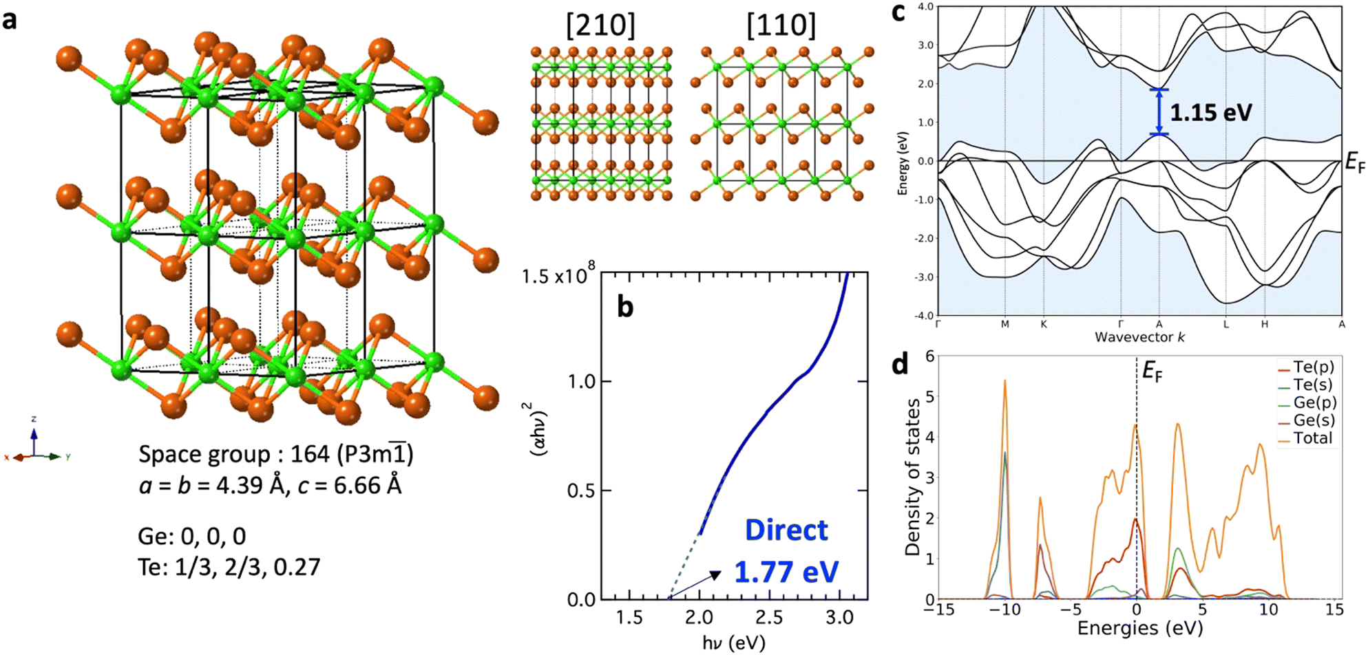 | ||
| Fig. 3 (a) Crystal structure model of GeTe2 from different angles. (b) Tauc plot of absorption spectra based on the assumption of direct transition. (c) Calculated band structure, where the energy zero corresponds to the Fermi level (EF). (d) Total and atom-projected DOS. | ||
The optical bandgap was determined from absorption spectra using a Tauc plot, as shown in Fig. 3b, based on the relationship (αhν)1/r = (const.)(hν − Eg), where α is the absorption coefficient, hν is the photon energy, and Eg is the optical bandgap.22 The raw optical data and the absorption coefficient calculation procedure are shown in the Fig. S5 (ESI†). The value of r differs depending on the material being an indirect (r = 2) or a direct (r = 1/2) transition semiconductor. As discussed in the next paragraph, the density functional theory (DFT) simulation suggests a direct transition; therefore, we introduced r = 1/2 for the Tauc plot. A value of 1.77 eV was obtained for the optical band gap assuming a direct transition. Comparing these values with those of other well-known semiconductors (1.1 eV for Si, 1.3 eV for typical TMD MoS2,23 and 1.0 eV for MoTe224) suggests that GeTe2 has great potential for application in electronics and optoelectronics. This bandgap is consistent with the high electrical resistance shown in Fig. 2b.
The band structure and density of states (DOS) were simulated using this model. The calculated band structure shown in Fig. 3c, at a first glance, exhibits metallic properties with the Fermi level (EF: E = 0) inside the valence band. This is a typical feature of metals, while an energy gap of approximately 0.5 eV is present above EF. The direct gap was approximately 1.15 eV at point A, which is slightly smaller than the value obtained from optical measurements, as shown in Fig. 3b. This can be understood by considering the well-known band gap underestimation in DFT simulations. The use of a hybrid calculation may yield a more appropriate value; however, because EF resides in the valence band, the use of a hybrid calculation alone may not be sufficient to resolve the inconsistency. For such materials to exhibit semiconducting properties (electrically and optically), one plausible explanation is that the real sample is naturally doped; here, donors are the major impurities that generate electrons, shifting the Fermi level toward the conduction band.
The atom-projected (P)DOS is shown in Fig. 3d. The relatively deep states at −7.5 and −10 eV mainly originate from Ge-s and Te-s states, respectively, similar to monotelluride GeTe.25 The valence band was composed of Ge-p and Te-p states; intriguingly, the contribution of the Ge-s states was clearly visible at the valence band maximum above the predicted Fermi level. This is an unusual feature in that for typical IV–VI compounds, the valence band maximum is formed from p-states. Future studies, including the effects of defects and stress, may provide useful insights, leading to a deeper understanding of the electronic structure of GeTe2.
Semiconductor device demonstration
Finally, we demonstrate the feasibility of GeTe2 as a semiconductor device using two different device structures. The first example is a two-terminal vertical device with top and bottom electrodes, where the linear ohmic I–V characteristics would be expected for metallic materials, while the I–V curve exhibits nonlinear behavior when a semiconductor material is sandwiched between them. Fig. 4(a) shows I–V curves, where the GeTe2 layer was sandwiched between two W electrodes with a contact size of 5 × 5 μm. Experimental I–V curves, repeated at least five times, showed nonlinear behavior. The obtained I–V curve cannot be fitted using a typical conduction mechanism for a Schottky contact (metal–semiconductor contact), but rather resembles typical Ovonic threshold switching (OTS) material.26 Generally, OTS behavior is observed in amorphous chalcogenides, in which localized carriers hop between defects in the sub-threshold region, while the application of voltage above the threshold voltage (Vth) results in a sudden increase in current due to delocalized carriers. For the Ge–Te binary system, amorphous GeTe6 (Ge14Te86) is the best-known OTS material, while other compositions have been less intensively studied.27 Surprisingly, the present OTS-like nonlinear I–V curve was obtained from a crystalline phase. The formation of a GeTe2 layer on the W bottom electrode was confirmed using XRD before patterning the top electrode (Fig. S6, ESI†). The origin of the OTS-like I–V behavior in GeTe2 is not clear currently; however, it is anticipated that localized defects may play an important role, similar to conventional OTS materials. The presence of a vareity of defects is plausible because GeTe2 is a metastable phase originating from a disordered amorphous phase. This also supports the reason why the experimentally observed band gap was not reproduced by DFT simulations for the intrinsic model, and the assumption of positive defects generating excess electrons could explain the shift of the Fermi level toward the band gap, resulting in semiconducting behavior. Fig. S7 (ESI†) shows the observed nonlinear I–V behavior for both polarities of the applied voltage. | ||
| Fig. 4 I–V characteristics of (a) a two-terminal vertical device and (b) a three-terminal lateral device. | ||
We also demonstrate a three-terminal transistor-like lateral device. In Fig. 4(b), the inset shows an optical microscopy image, where the GeTe2 layer was used as a channel between the source and drain top electrodes. The channel length was 48 μm, and the gate voltage was applied from the substrate back electrode. The Id–Vg curve demonstrates typical p-type channel transistor behavior. This is consistent with the above discussion, in which the Fermi level is shifted up from inside of the valence band to around the valence band maximum to form a p-type semiconductor. Notably, the as-fabricated device showed broad Id–Vg switching with a small on/off ratio. The Id–Vg curve improved significantly with post-annealing after device fabrication. The maximum post-annealing temperature was 230 °C, the highest temperature possible before phase separation of GeTe2 into crystalline GeTe + Te occurs, which shows metallic behavior and no change with respect to the gate voltage. The 230 °C-annealed device demonstrated much sharper switching with a three-order on/off ratio. The effect of post-annealing can be explained based on the improvement in the contact between the GeTe2 semiconductor and W metal electrodes often observed for Si transistors as well as state-of-the-art two-dimensional transistor devices.
Specifically, the above two devices do not demonstrate performance comparable to the best modern OTS and transistor devices at present. However, the discovery of a “metastable” van der Waals material strongly underscores the nature of such unexplored materials that have the potential to demonstrate unique and superior properties over those of known “stable” layered materials.
Experimental
Sample preparation
Ge–Te films were deposited on Si, Si/thermal SiO2 (100 nm), SiO2, and Al2O3 substrates via radio frequency (RF) magnetron sputtering using GeTe and Te targets. The composition of the films was controlled by tuning the relative sputtering power. The base pressure of the chamber was below 4.0 × 10⁻⁵ Pa, and the working pressure was set to 4.0 × 10⁻¹ Pa by introducing Ar gas at a flow rate of 48.9 sccm. The as-deposited amorphous thin films were crystallized via thermal annealing. Before annealing, the sample chamber was evacuated below 5.0 × 10⁻³ Pa, and then Ar was backfilled to a pressure of 1.0 × 10⁵ Pa.Resistance-temperature measurements
The temperature dependence of the electrical resistance during heating and cooling was measured using the two-point probe method. The heating rate was 10 °C min−1, and the chamber was backfilled with an Ar atmosphere at 1 atm after evacuation.X-Ray diffraction (XRD)
The crystal structures of the samples were analyzed through XRD, wherein Cu-Kα (λ = 0.1542 nm) was used as the X-ray source and a symmetric scan (Bragg-Brentano geometry) was employed (Ultima IV, Rigaku Corp.).Optical measurements
The reflectance and transmittance of the films grown on the SiO2 substrates were measured using a spectrophotometer (V-630BIO, JASCO Corp.).Transmission electron microscopy (TEM)
TEM measurements were performed to observe the microstructure using an aberration-corrected transmission electron microscope (JEM-ARM200F, JEOL Co. Ltd) operated at an acceleration voltage of 200 kV. Energy-dispersive X-ray spectroscopy (EDX) measurements were performed using the scanning TEM mode of the microscope. Cross-sectional TEM sample preparation was performed using a focused ion beam (NB5000, Hitachi High Technologies, Inc.).Simulation of the crystal structure
Crystal structure images were generated using CrystalMaker®, a crystal and molecular structure program for Mac and Windows. The XRD patterns were generated using CrystalDiffract®, a powder diffraction program for Mac and Windows. Both are published by CrystalMaker Software Ltd, Oxford, England (https://www.crystalmaker.com).Density functional theory (DFT) simulation
The electronic structure was simulated using the PBE functional implemented in the Vienna ab initio simulation package (VASP).28–30 A plane-wave basis set was used with projector-augmented wave (PAW) pseudopotentials. The Ge and Te pseudopotentials included Ge:3d104s24p2 and Te:5s25p4 valence electrons. The energy cut-off was set to 400 eV, and an energy convergence of 10−5 eV was used. Furthermore, a 12 × 12 × 8 Monkhorst–Pack grid was used.31 The band structure and DOS were plotted using pymatgen.32Device fabrication and electrical measurements
For vertical two-terminal devices, the bottom W (50 nm) and SiO2 (50 nm) layers were deposited sequentially without breaking the vacuum. Photoresist was spin-coated and a 5 × 5 μm square region was irradiated with UV light to remove the resist. Subsequently, the SiO2 layer was wet-etched using a buffered HF solution. A Ge0.33Te0.67 (50 nm) film was deposited and annealed to form the GeTe2 phase. After confirming the sample structure via XRD (Fig. S5, ESI†), the top W electrode (50 nm) pattern was fabricated using the deposition and lift-off processes to form individual devices. The lateral three-terminal devices were fabricated using a similar technique. Note that after the fabrication of the GeTe2-based transistor, post-annealing was performed to improve the electrical contact between the W electrode and GeTe2. For the transistor device, a highly doped n-type Si substrate was used to realize a back-gate-type structure.Conclusions
Herein, polymorphic crystallization was used as a novel synthesis technique to fabricate MVMs. As an example, an amorphous Ge0.33Te0.67 film was initially prepared by sputtering. Subsequent annealing under optimal conditions resulted in the formation of the MVM, GeTe2. Intriguingly, unexpected semiconducting properties were confirmed via multiple experiments, underscoring the significance of this technique. Attempts to model the metastable crystalline phase using DFT calculations with an experimentally determined unit cell indicated that the system was metallic because the Fermi level was located in the valence band. It is suggested that electrons originating from point defects result in the Fermi level moving into the gap, leading to the observed semiconducting behavior. Additionally, the necessity of stress for the formation of the metastable phase was experimentally confirmed, a condition often overlooked in data-oriented high-throughput simulations. This paper demonstrates an important proof of concept for the growth of MVMs via polymorphic crystallization. Although realizing an atomic-level monolayer device is one of the most important applications involving layered materials, the present work is limited to 50 nm-thick films. Therefore, investigations on monolayer GeTe2 are strongly desired in the future. The technique is expected to facilitate the investigation of a wide range of unexplored metastable functional materials for future electronics applications.Conflicts of interest
There are no conflicts to declare.Acknowledgements
This study was supported by JSPS KAKENHI (Grant No. 18K14306, 19H02619, and 21H05009) and partially by the commissioned research (No. 03701) of the National Institute of Information and Communications Technology (NICT), Japan. We thank Prof. Alexander V. Kolobov for the fruitful discussions. XRD was conducted at the AIST Nano-Processing Facility (NPF). The TEM measurements were supported by the NIMS microstructural characterization platform (NMCP). We thank Ms. Miho Sakurai (AIST) for her technical assistance.References
- K. S. Novoselov, A. K. Geim, S. V. Morozov, D. Jiang, Y. Zhang, S. V. Dubonos, I. V. Grigorieva and A. A. Firsov, Electric field effect in atomically thin carbon films, Science, 2004, 306(5696), 666–669, DOI:10.1126/science.1102896.
- S. Das, A. Sebastian, E. Pop, C. J. McClellan, A. D. Franklin, T. Grasser, T. Knobloch, Y. Illarionov, A. V. Penumatcha, J. Appenzeller, Z. Chen, W. Zhu, I. Asselberghs, L.-J. Li, U. E. Avci, N. Bhat, T. D. Anthopoulos and R. Singh, Transistors based on two-dimensional materials for future integrated circuits, Nat. Electron., 2021, 4(11), 786–799, DOI:10.1038/s41928-021-00670-1.
- A. Zavabeti, A. Jannat, L. Zhong, A. A. Haidry, Z. Yao and J. Z. Ou, Two-dimensional materials in large-areas: Synthesis, properties and applications, Nano-Micro Lett., 2020, 12(1), 66, DOI:10.1007/s40820-020-0402-x.
- S. Hussain, J. Singh, D. Vikraman, A. K. Singh, M. Z. Iqbal, M. F. Khan, P. Kumar, D.-C. Choi, W. Song, K.-S. An, J. Eom, W.-G. Lee and J. Jung, Large-area, continuous and high electrical performances of bilayer to few layers MoS2 fabricated by rf sputtering via post-deposition annealing method, Sci. Rep., 2016, 6, 30791, DOI:10.1038/srep30791.
- J.-H. Huang, K.-Y. Deng, P.-S. Liu, C.-T. Wu, C.-T. Chou, W.-H. Chang, Y.-J. Lee and T.-H. Hou, Large-area 2D layered MoTe2 by physical vapor deposition and solid-phase crystallization in a tellurium- free atmosphere, Adv. Mater. Interfaces, 2017, 4(17), 1700157, DOI:10.1002/admi.201700157.
- C.-C. Chiang, V. Ostwal, P. Wu, C.-S. Pang, F. Zhang, Z. Chen and J. Appenzeller, Memory applications from 2D materials, Appl. Phys. Rev., 2021, 8(2), 021306, DOI:10.1063/5.0038013.
- F. Zhang, H. Zhang, S. Krylyuk, C. A. Milligan, Y. Zhu, D. Y. Zemlyanov, L. A. Bendersky, B. P. Burton, A. V. Davydov and J. Appenzeller, Electric-field induced structural transition in vertical MoTe2- and Mo1−xWxTe2-based resistive memories, Nat. Mater., 2019, 18(1), 55–61, DOI:10.1038/s41563-018-0234-y.
- M. Wuttig and N. Yamada, Phase-change materials for rewriteable data storage, Nat. Mater., 2007, 6(11), 824–832, DOI:10.1038/nmat2009.
- P. Noé, C. Vallée, F. Hippert, F. Fillot and J.-Y. Raty, Phase-change materials for non-volatile memory devices: from technological challenges to materials science issues, Semicond. Sci. Technol., 2018, 33(1), 013002, DOI:10.1088/1361-6641/aa7c25.
- R. E. Simpson, P. Fons, A. V. Kolobov, T. Fukaya, M. Krbal, T. Yagi and J. Tominaga, Interfacial phase-change memory, Nat. Nanotechnol., 2011, 6(8), 501–505, DOI:10.1038/nnano.2011.96.
- M. S. Choi, B.-K. Cheong, C. H. Ra, S. Lee, J.-H. Bae, S. Lee, G.-D. Lee, C.-W. Yang, J. Hone and W. J. Yoo, Electrically driven reversible phase changes in layered In2Se3 crystalline film, Adv. Mater., 2017, 29(42), 1703568, DOI:10.1002/adma.201703568.
- S. Mori, S. Hatayama, Y. Shuang, D. Ando and Y. Sutou, Reversible displacive transformation in MnTe polymorphic semiconductor, Nat. Commun., 2020, 11(1), 85, DOI:10.1038/s41467-019-13747-5.
- J. Wang, I. Ronneberger, L. Zhou, L. Lu, V. L. Deringer, B. Zhang, L. Tian, H. Du, C. Jia, X. Qian, M. Wuttig, R. Mazzarello and W. Zhang, Unconventional two-dimensional germanium dichalcogenides, Nanoscale, 2018, 10, 7363–7368, 10.1039/C8NR01747F.
- H. Fukumoto, K. Tsunetomo, T. Imura and Y. Osaka, Structural changes of amorphous GeTe2 films by annealing (formation of metastable crystalline GeTe2 films), J. Phys. Soc. Jpn., 1987, 56(1), 158–162, DOI:10.1143/JPSJ.56.158.
- H. Okamoto, Ge-Te (Germanium-Tellurium), J. Phase Equilib., 2000, 21(5), 496, DOI:10.1361/105497100770339789.
- T. Siegrist, P. Jost, H. Volker, M. Woda, P. Merkelbach, C. Schlockermann and M. Wuttig, Disorder-induced localization in crystalline phase-change materials, Nat. Mater., 2011, 10(3), 202, DOI:10.1038/nmat2934.
- K. Tsunetomo, T. Sugishima, T. Imura and Y. Osaka, Stability of metastable GeTe2 in thin films, J. Non-Cryst. Solids, 1987, 95–96, 509–516, DOI:10.1016/S0022-3093(87)80151-5.
- Y. Saito, M. Morota, K. Makino, J. Tominaga, A. V. Kolobov and P. Fons, Recent developments concerning the sputter growth of chalcogenide-based layered phase-change materials, Mater. Sci. Semicond. Process., 2021, 135, 106079, DOI:10.1016/j.mssp.2021.106079.
- A. V. Kolobov and J. Tominaga, Two-Dimensional Transition-Metal Dichalcogenides, Springer International Publishing, 1st edn, 2016, 239 DOI:10.1007/978-3-319-31450-1_3.
- S. Hatayama, Y. Saito, K. Makino, N. Uchida, Y. Shuang, S. Mori, Y. Sutou, M. Krbal and P. Fons, Phase control of sputter-grown large-area MoTe2 films by preferential sublimation of Te: amorphous, 1T’ and 2H phases, J. Mater. Chem. C, 2022, 10, 10627, 10.1039/D2TC01281B.
- A. Tverjanovich, M. Khomenko, C. J. Benmore, M. Bokova, A. Sokolov, D. Fontanari, M. Kassem, T. Usuki and E. Bychkov, Bulk glassy GeTe2: A missing member of the tetrahedral GeX2 family and a precursor for the next generation of phase-change materials, Chem. Mater., 2021, 33, 1031, DOI:10.1021/acs.chemmater.0c04409.
- J. Tauc, R. Grigorovici and A. Vancu, Optical properties and electronic structure of amorphous Germanium, Phys. Status Solidi B, 1966, 15(2), 627–637, DOI:10.1002/pssb.19660150224.
- K. F. Mak, C. Lee, J. Hone, J. Shan and T. F. Heinz, Atomically thin MoS2: a new direct-gap semiconductor, Phys. Rev. Lett., 2010, 105, 136805, DOI:10.1103/PhysRevLett.105.136805.
- C. Ruppert, O. B. Aslan and T. F. Heinz, Optical properties and band gap of single- and few-layer MoTe2 crystals, Nano Lett., 2014, 14(11), 6231–6236, DOI:10.1021/nl502557g.
- J.-J. Kim, K. Kobayashi, E. Ikenaga, M. Kobata, S. Ueda, T. Matsunaga, K. Kifune, R. Kojima and N. Yamada, Electronic structure of amorphous and crystalline (GeTe)1−x(Sb2Te3)x investigated using hard x-ray photoemission spectroscopy, Phys. Rev. B: Condens. Matter Mater. Phys., 2007, 76, 115124, DOI:10.1557/PROC-1072-G02-07.
- M. Zhu, K. Ren and Z. Song, Ovonic threshold switching selectors for three-dimensional stackable phase-change memory, MRS Bull., 2019, 44(9), 715–720, DOI:10.1557/mrs.2019.206.
- M. Anbarasu, M. Wimmer, G. Bruns, M. Salinga and M. Wuttig, Nanosecond threshold switching of GeTe6 cells and their potential as selector devices, Appl. Phys. Lett., 2012, 100(14), 143505, DOI:10.1063/1.3700743.
- J. P. Perdew, K. Burke and M. Ernzerhof, Generalized gradient approximation made simple, Phys. Rev. Lett., 1996, 77(18), 3865–3868, DOI:10.1103/PhysRevLett.77.3865.
- G. Kresse and J. Furthmüller, Efficiency of ab-initio total energy calculations for metals and semiconductors using a plane-wave basis set, Comput. Mater. Sci., 1996, 6(1), 15–50, DOI:10.1016/0927-0256(96)00008-0.
- G. Kresse, & Furthmüller, J. Efficient iterative schemes for ab initio total-energy calculations using a plane-wave basis set, Phys. Rev. B: Condens. Matter Mater. Phys., 1996, 54, 11169–11186, DOI:10.1103/PhysRevB.54.11169.
- H. J. Monkhorst and J. D. Pack, Special points for Brillouin-zone integrations, Phys. Rev. B: Solid State, 1976, 13(12), 5188–5192, DOI:10.1103/PhysRevB.13.5188.
- S. P. Ong, W. D. Richards, A. Jain, G. Hautier, M. Kocher, S. Cholia, D. Gunter, V. L. Chevrier, K. A. Persson and G. Ceder, Python materials genomics (pymatgen): a robust, open-source python library for materials analysis, Comput. Mater. Sci., 2013, 68, 314–319, DOI:10.1016/j.commatsci.2012.10.028.
Footnote |
| † Electronic supplementary information (ESI) available. See DOI: https://doi.org/10.1039/d2mh01449a |
| This journal is © The Royal Society of Chemistry 2023 |