
Green-solvent-processed formamidinium-based perovskite solar cells with uniform grain growth and strengthened interfacial contact via a nanostructured tin oxide layer†
Xueyun
Wu
,
Yiting
Zheng
,
Jianghu
Liang
,
Zhanfei
Zhang
,
Congcong
Tian
,
Zhiang
Zhang
,
Yixuan
Hu
,
Anxin
Sun
,
Chenyang
Wang
,
Jianli
Wang
,
Ying
Huang
,
Zhifu
Zhang
,
Kolan Madhav
Reddy
 * and
Chun-Chao
Chen
*
* and
Chun-Chao
Chen
*
School of Materials Science and Engineering, Shanghai Jiao Tong University, Shanghai 200240, P. R. China. E-mail: kmreddy@sjtu.edu.cn; c3chen@sjtu.edu.cn
First published on 18th October 2022
Abstract
Green-solvent-processed perovskite solar cells (PSCs) have reached an efficiency of 20%, showing great promise in safe industrial production. However, the nucleation process in green-solvent-based deposition is rarely optimized, resulting in randomized crystallization and much lowered reported efficiencies. Herein, a nanostructured tin oxide nanorods (SnO2-NRs) substrate is utilized to prepare a high-quality formamidinium (FA)-based perovskite film processed from a green solvent of triethyl phosphate (TEP) with a low toxic antisolvent of dibutyl ether (DEE). Compared with SnO2 nanoparticles, the oriented SnO2-NRs can accelerate the formation of heterogeneous nucleation sites and retard the crystal growth process of the perovskite film, resulting in a high-quality perovskite film with uniform grain growth. Furthermore, a chlorine-terminated bifunctional supramolecule (Cl-BSM) is introduced to passivate the increasing interfacial defects due to the vast contact area in SnO2-NRs. Correspondingly, the substrate design of SnO2-NRs with Cl-BSM increases the power conversion efficiency (PCE) of green-solvent-processed PSCs to 22.42% with an open-circuit voltage improvement from 1.02 to 1.12 V, which can be attributed to the uniform grain growth and reduced carrier recombination at the SnO2-NRs/perovskite interface. More importantly, the photo and humidity stabilities of the unencapsulated device for up to 500 and 1000 hours are also achieved with negligible interfacial delamination after aging. This work provides a new perspective on the future industrial scale production of PSCs using environment-friendly solvents with compatible substrate design.
New conceptsFormamidinium (FA)-based perovskite solar cells (PSCs) have reached a record-high efficiency of up to 25.7%, showing great potential in future industrial commercialization. Nevertheless, the utilization of all-green solvent processing toward high efficiency FA-based PSCs still remains challenging. Besides, the nucleation process of the perovskite film with green-solvent-based deposition is rarely optimized, resulting in randomized crystallization and much lowered reported efficiencies. In this work, we propose a new concept using nanostructured tin oxide nanorods (SnO2-NRs) substrate to accelerate the formation of heterogeneous nucleation sites and retard the crystal growth process of the perovskite film. By utilizing triethyl phosphate (TEP) as a green host solvent and dibutyl ether (DEE) as a low toxic antisolvent, a high quality FA-based perovskite film based on the SnO2-NR substrate with uniform grain growth is achieved. Furthermore, the substrate design of SnO2-NRs with a chlorine-terminated bifunctional supramolecule achieves a high power conversion efficiency of green-solvent-processed PSCs of 22.42%. We therefore provide a new perspective on the future industrial scale production of PSCs using environment-friendly solvents with compatible substrate design. |
1. Introduction
Organometallic-halide perovskite solar cells (PSCs) are emerging as the most promising next generation solar cell devices due to the properties of high light-absorption coefficient and high power conversion efficiency (PCE).1–3 Among various perovskite absorbers, formamidinium (FA)-based perovskite has reached a record-high efficiency of up to 25.7%, showing great potential in future industrial commercialization.4 Generally, solvent engineering by Lewis-base solvent and anti-solvent is the most commonly used for the fabrication of high-performance PSCs.5,6 However, all current highest performance PSCs are strongly depending on the usage of these toxic solvents, e.g. N,N-dimethylformamide (DMF) and chlorobenzene (CB), which might threaten the safety of environments with the commercialization of PSCs in the future.7,8 Therefore, it is urgent to develop a green-solvent-based fabrication process for reducing the detrimental effect on both human health and the environment.To date, several green solvents have been studied to replace the toxic ones. However, research studies are mainly focusing on greener antisolvent replacement as shown in Table S1 (ESI†).9–16 Inversely, there are few reports on developing green host solvents to replace toxic solvents like DMF, owing to the low solubility of perovskite precursors in common green solvents. To overcome the solubility issue, dimethyl sulfoxide (DMSO) with a high donor number and high coordination ability is used as the green solvent for the perovskite precursor.17–19 Nevertheless, owing to its non-volatility, DMSO failed to achieve a pinhole-free morphology with high crystallinity in perovskite films when used alone as a processing solvent.20 Besides DMSO, 2-methoxyethanol (2-Me) with lower toxicity was also used to replace DMF in many large-area fabrication processes of PSCs.21–26 Without strong coordination ability, 2-Me often requires other toxic solvent additives, such as acetonitrile (ACN)22 and N-methylpyrrolidone (NMP),23 to achieve a desirable film morphology and device performance. Recently, a new family of greener solvents, triethyl phosphate (TEP) and trimethyl phosphate (TMP),27,28 show comparable dissolving ability for perovskite precursors. Yun et al.28 reported that TMP-derived PSCs exhibited the best PCE of 20.02%. Similarly, Cao et al.27 used TEP to deposit FA-based perovskite layers, resulting in a champion PCE of 20.13%. Moreover, volatile perovskite ink is obtained by dissolving the precursor in a mixed solvent system consisting of a volatile solvent (such as ethanol, tetrahydrofuran, ACN) and lots of ammonium salt to control the nucleation/crystallization process.29,30 Among these green-solvent fabrication processes, the weak intermediate phase and correspondingly uncontrolled nucleation process are commonly found and limit the crystal quality of perovskite thin films. To overcome these bottlenecks, a new substrate design with the ability to control the nucleation process of high-quality perovskite films should be considered.
The electron transport layer (ETL), as a substrate of regular PSC architecture, has a great effect on the crystallization characteristics and chemical nucleation of the perovskite film.31–33 Park group33 has reported the importance of the ETL geometry for maximizing the device performance. Generally, the mesoporous ETL can provide numerous heterogeneous nucleation sites, facilitating the formation of perovskite films with better crystalline quality and uniform coverage.34,35 In particular, an ETL with a one-dimensional (1D) nanostructure, is expected to boost charge extraction and facilitate high-quality perovskite crystal growth.36–41 Zhong et al.40 demonstrated that TiO2 nanocorns can extract electrons quickly to suppress charge recombination. Lv et al.41 reported that TiO2 nanopyramid arrays are excellent building blocks for high-performance PSCs with efficiency comparable to those of typical mesoscopic and planar PSCs. While the TiO2 ETL is sensible to ultraviolet light due to the unwanted photocatalytic effects. Recently, tin oxide (SnO2), with less photocatalytic degradation and a favorable conduction band edge, is considered as a promising and effective ETL candidate to replace TiO2. Sun et al. proposed antimony-doped SnO2 nanorods (SnO2-NRs) as a novel transparent conductive mesoporous layer to achieve micrometer-sized grains and the ultrasmooth surface of the perovskite film.37 Therefore, the use of a nanostructured substrate is expected to be a new approach for fabricating high-quality FA-based perovskite films with green solvents. Additionally, owing to the large contact area and numerous hydroxyl groups at the SnO2-NRs interface, it inevitably shows extensive non-radiative recombination at the SnO2-NRs/perovskite interface. Therefore, in order to maximize the potential of SnO2-NRs, it is necessary to develop a more compatible interfacial modification molecule with defect passivation capability and a strong interfacial bonding force for improving device stability.
In this work, the SnO2-NRs substrate is proposed to explore the mechanism of nucleation and growth of a green-solvent-processed perovskite film by solving the weak intermediate phase and the uncontrolled nucleation process in green-solvent-based deposition. On the one hand, it can facilitate the nucleation process by supplying numerous heterogeneous nucleation sites with reduced Gibbs free energy. On the other hand, the uniform and large grains of green-solvent-processed perovskite are obtained via the Ostwald ripening process. In addition, a chlorine-terminated bifunctional supramolecule (Cl-BSM), 3-chloropropyl trimethoxysilane, is introduced to reduce interfacial defects and strengthen the contact strength via Si–O bonds and halogen (Pb–Cl) bonds. As a result, PSCs based on SnO2-NRs deliver an efficiency of up to 22.42%, which is a higher value for green-solvent-processed PSCs. Benefiting from the Cl-BSM modified SnO2-NRs substrate, the stability of PSCs is greatly improved with minimal damage accumulation at the SnO2-NRs/perovskite interface even after aging 1000 hours under ambient conditions.
2. Results and discussion
2.1 Characterization and crystal growth mechanism of an all-green perovskite film based on the SnO2-NRs substrate
Fig. 1a depicts the typical fabrication procedure of a FA-based perovskite film based on the all-green solvent engineering approach. The FA-based perovskite composition used here is (FAPbI3)0.95(MAPbBr3)0.05 with a bandgap of 1.56 eV. TEP is used as a single solvent for perovskite precursors, and DEE is used as an antisolvent with low toxicity. Since DMSO is unstable and can be easily oxidized, methylammonium chloride (MACl) is used instead as the intermediate-phase additive.16 Fig. S1 (ESI†) shows the X-ray diffraction (XRD) spectra of perovskite films processed from green-solvent (TEP) and toxic-solvent (DMF/DMSO) precursors, respectively. The result indicates that the perovskite film based on green solvent has poor crystallinity, which can be attributed to the uncontrolled crystallization process and weak intermediate phase for the DMSO-free precursor.42 Since the planar substrate can lead to quick crystal growth of the perovskite film and result in non-uniform grain growth, a new substrate design is proposed here. To assist the nucleation in all-green-solvent deposition, SnO2 nanorods (SnO2-NRs) are chosen as ETL scaffolds, which can supply numerous heterogeneous nucleation sites compared with planar SnO2 nanoparticles (SnO2-NPs),32,34 further resulting in the enhanced quality of the perovskite film and uniform perovskite coverage over large areas. The top-view scanning electron microscopy (SEM) images of the (FAPbI3)0.95(MAPbBr3)0.05 perovskite film based on SnO2 nanostructured nanorods and planar substrates are exhibited in Fig. 1a, respectively. It shows that the uniform grain growth with larger grains of the perovskite film is formed based on the SnO2-NRs substrate, while the perovskite film shows non-uniform grain growth based on the planar SnO2-NPs substrate. Moreover, the average grain size statistics of the perovskite are about 1.11 μm based on SnO2-NRs and about 0.72 μm based on SnO2-NPs (Fig. S2, ESI†). Therefore, a larger grain size of the perovskite film based on the SnO2-NRs substrate is obtained.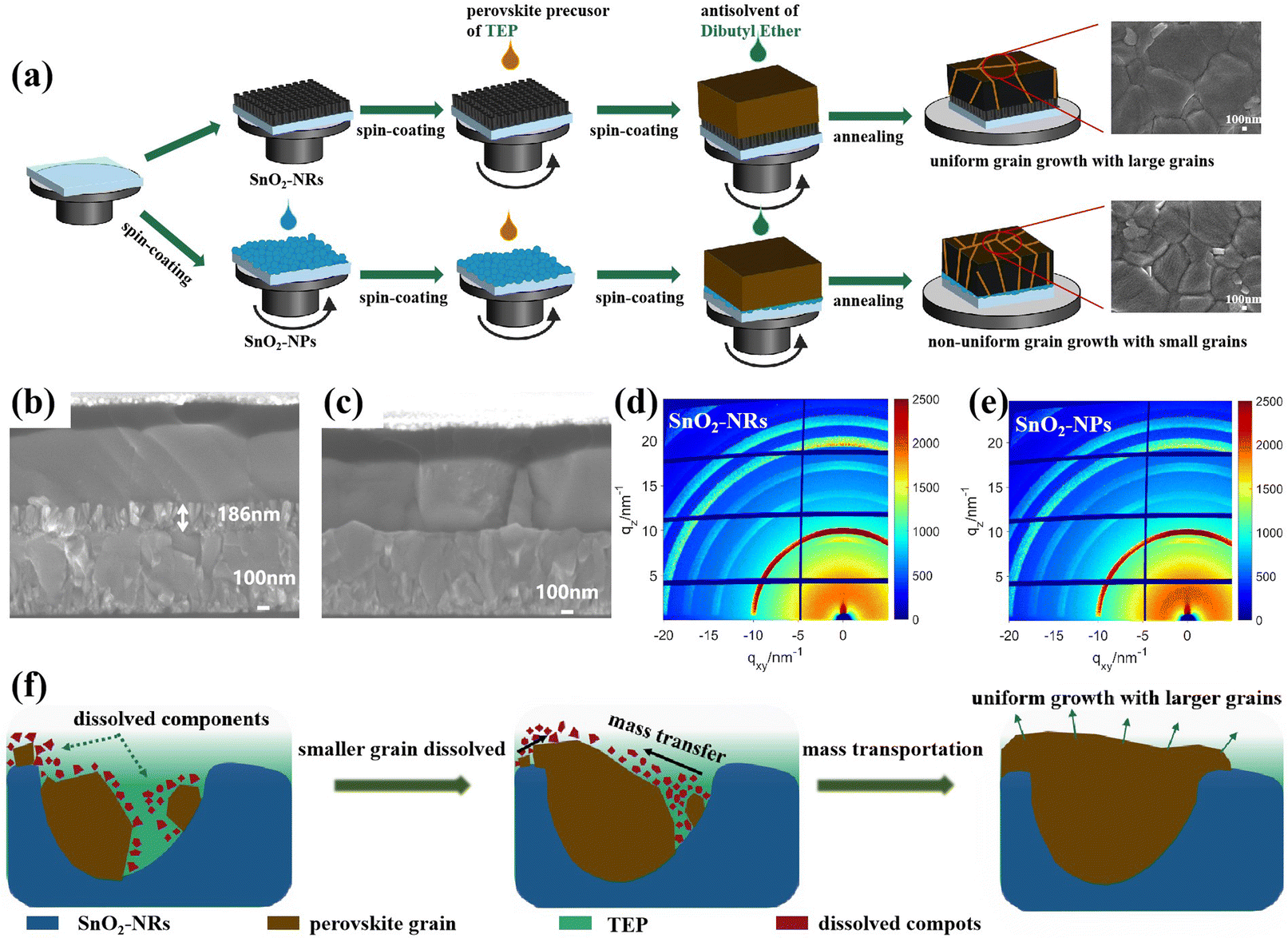 | ||
| Fig. 1 Characterization and crystal mechanism of the all-green perovskite film based on SnO2-NRs. (a) Schematic of the fabrication procedures of the green-solvent process of the perovskite based on SnO2-NRs and SnO2-NPs substrates, respectively. Inset images are top-view SEM images of the perovskite film based on SnO2-NRs and SnO2-NPs substrates. (b and c) Cross-sectional SEM images of the perovskite film based on (b) SnO2-NRs and (c) SnO2-NPs, respectively. (d and e) 2D GIWAXS patterns of the perovskite film deposited on (d) SnO2-NRs and (e) SnO2-NPs coated quartz substrates. (f) Schematic diagram of the Ostwald ripening procedures during the nucleation process. | ||
The cross-sectional SEM images (Fig. 1b and c) of the perovskite film based on SnO2-NRs and SnO2-NPs exhibit a more significant difference in grain sizes along the vertical direction of perovskite growth. It shows that the SnO2-NRs substrate yields uniform grain growth with larger grains and more vertically penetrating perovskite grains in the entire perovskite film compared to that of the SnO2-NPs substrate, which is consistent with the results of top-view SEM images. Compared with the SnO2-NPs substrate, SnO2-NRs show a smaller contact angle of 12.2° in Fig. S3 (ESI†), resulting in the enhanced wettability of the SnO2 interface for the deposition of the perovskite film. In addition, a smaller contact angle can result in reduced Gibbs free energy, thus assisting the nucleation process.43 This suggests that the SnO2-NRs substrate can provide low surface energy for heterogeneous nucleation, thus obtaining a perovskite film with increased grain size. Grazing incidence wide-angle X-ray scattering (GIWAXS) measurements (Fig. 1d and e) are further used to examine the crystallographic orientations of the perovskite film based on SnO2-NRs and SnO2-NPs substrates, respectively. The 2D GIWAXS patterns of the perovskite film on ETL-coated quartz substrates display typical scattering rings of about 10 nm−1 and 20 nm−1, which correspond to the (110) and (220) planes,44 respectively. In particular, compared to the SnO2-NPs substrate, the perovskite film based on SnO2-NRs shows the highest diffraction (110) peak intensity at qz = 10 nm−1 in Fig. S4 (ESI†), which is assigned to the black phase FAPbI3. This indicates that the perovskite film shows a stronger orientational preference that is perpendicular to the SnO2-NRs substrate, resulting in the high crystallization orientation of the perovskite film.
In order to explore the relationship of the crystallization kinetics between the perovskite film and SnO2-NRs, the Ostwald ripening model is introduced as shown in Fig. 1f.45 Owing to the lower nucleation energy barrier at the heterogeneous interface of ETL/perovskite than that at the homogeneous interface, SnO2-NRs can provide numerous heterogeneous nucleation sites that facilitate the nucleation of perovskite grains. During the nucleation process, perovskite precursors with different particle sizes are initially formed on the SnO2-NRs substrate. Besides, it has been reported that the particle chemical potential is inversely proportional to the particle radius.42 Thus, a smaller particle is energetically less stable due to the higher chemical potential, and it will be easily dissolved if there is a sufficient amount of solvent presented. According to Fick's first law,46 the dissolved components of small perovskite grains will lead to a concentration gradient between the small grains and the large grains, which further results in the mass transportation from small grains to the larger ones. During the annealing procedure, the SnO2-NRs with nanostructured arrays would inevitably delay the extraction of the perovskite precursor solvent and prolong the ripening of the (FAPbI3)0.95(MAPbBr3)0.05 precursor to form larger perovskite crystals. As the annealing time proceeds, the smaller grains begin to fuse into larger ones. As a result, the high-crystallinity perovskite film with micro-sized grains is obtained via mass transportation (Fig. 1f). In contrast, the solvent molecules are extracted more easily from the precursor films based on the planar SnO2-NPs substrate, which leaves less time for the Ostwald ripening process and leads to smaller perovskite grains. This indicates that the fast heterogeneous nucleation process and retarded crystal growth are the key to forming larger perovskite crystals based on the SnO2-NRs substrate.
In addition, the optical property and structure of the ETL substrate play an important role in the morphology and crystallinity of perovskite film. Therefore, the optical and morphology properties of nanostructured SnO2-NRs are further explored. The UV-vis transmission and diffuse reflectance spectra are recorded to compare the optical properties of bare FTO glass, FTO/SnO2-NPs, and FTO/SnO2-NRs. The higher transmittance of the three SnO2-NRs compared to the bare FTO glass indicates the antireflection capability of SnO2-NRs (Fig. S5, ESI†).41,47 Besides, the higher transmittance of SnO2-NRs can also be easily distinguished from the optical image of the Fig. S5 (ESI†) inset by its appearance. Therefore, the SnO2-NRs substrate allows more photons to be absorbed by the perovskite film to achieve stronger light-harvesting for PSCs.48 The diffuse reflectance spectra of different films (Fig. S6, ESI†) also demonstrate the high light scattering capability of SnO2-NRs.42,49
Fig. S7a (ESI†) shows the schematic diagram for the preparation procedures of SnO2-NRs on a FTO substrate. The details are described in the Experimental section. Owing to the sensibility of the reaction temperature, SnO2-NRs show different morphologies at 180 °C (denoted as NRs-i), 200 °C (denoted as NRs-ii) and 220 °C (denoted as NRs-iii). The transmission electron microscopy (TEM) and high-resolution TEM (HR-TEM) images of NRs-ii are firstly carried out as shown in Fig. S8 (ESI†), where the NRs-ii sample exhibits a high degree of crystallization with a spacing of 0.34 nm between the lattice planes, which is consistent with rutile SnO2.50 High-angle annular dark-field scanning transmission electron microscopy (HAADF-STEM) and energy dispersive X-ray (EDX) mapping are further carried out to confirm the chemical composition of SnO2-NRs (Fig. S9, ESI†), where the SnO2-NRs show only O and Sn elements. The top-view and cross-sectional SEM images of SnO2-NRs at different reaction temperatures are further carried out as shown in Fig. S7 (ESI†). The NRs-i ETL layer exhibits uneven and sparse nanorod arrays (Fig. S7b, ESI†), which would lead to leakage current originating from direct contact between the perovskite layer and the FTO substrate. Correspondingly, the perovskite film with a pinhole morphology is observed in Fig. S10a (ESI†).
From the photovoltaic parameters shown in Table S2 (ESI†), the performance of PSCs with 15.63% based on the NRs-i ETL layer shows the lowest open-voltage (Voc) and fill factor (FF) owing to the imperfect interface of the NRs-i/perovskite film. Nevertheless, the length–diameter ratio of the three SnO2-NRs is increased when the reaction temperature changed from 180 °C to 220 °C. Fig. S7d (ESI†) shows the NRs-iii ETL with the largest length–diameter ratio, leading to more-effective perovskite infiltration but resulting in an inferior performance with 18.09% (Table S2, ESI†). Since the NRs-iii ETL has the longest nanorod length and the highest thickness among the three samples, the distance of electron transport may be too long to be effective.51 Furthermore, smaller grains and textured surface is also found in Fig. S10b (ESI†). Inversely, NRs-ii shows an even surface morphology (Fig. S7c, ESI†) for the smooth and pinhole-free perovskite film as shown in Fig. S2a (ESI†). As a result, the PSCs based on NRs-ii show a highest PCE of 19.30% among the three SnO2-NRs substrates as shown in Fig. S11 (ESI†). This improvement can be attributed to the efficient carrier transportation and improved pore-filling of the perovskite film on the NRs-ii ETL. However, compared with the SnO2-NRs, PSCs based on the SnO2-NP exhibit a lowest short-circuit current density (Jsc) of 23.66 mA cm−2 and efficiency of 19.17%, which may be caused by the irregular orientation structure that further leads to a scattering of free electrons and the decreased charge extraction efficiency. These results indicate that the SnO2-NRs ETL with a unique vertically oriented 1D nanostructure can enhance efficient light harvesting and facilitate carrier transformation. Therefore, the following work will use NRs-ii with 186 nm length as the ETL substrate unless otherwise noted.
2.2 The strengthened interfacial contact of the perovskite film based on the Cl-BSM modified SnO2-NRs substrate
To further enhance the performance of PSCs, one must improve the interfacial contact between the SnO2-NRs substrate and the perovskite layer for reducing interfacial defects. Herein, (3-chloropropyl)trimethoxysilane [Si(OCH3)3(CH2)3Cl], as a bifunctional supramolecule (denoted as Cl-BSM hereafter), is introduced to strengthen the interaction at the interface between SnO2-NRs and the perovskite film (Fig. 2a). The Cl-BSM is deposited on the surface of SnO2-NRs by dip-coating at room temperature. Besides, density functional theory (DFT) calculations are performed to examine the interface bonding by Cl-BSM interpenetration at the Cl-BSM/perovskite interface. H-BSM with a –H terminal group [Si(OCH3)3(CH2)3H] is used as a control sample to further prove the effects of the –Cl terminal group. The interfacial binding energy (Eint) and bond formation of H(CH2)4Cl and H(CH2)4H interfaced with different terminated perovskite (001) surfaces are shown in Table S3 and Fig. S12 (ESI†), respectively. Table S3 (ESI†) shows that the PbI2-terminated perovskite (001) surface with H(CH2)4Cl exhibits the highest Eint (0.466 eV), indicating that the perovskite film with a PbI2-terminated interface is favorable for coming into contact with H(CH2)4Cl. As reported that halogen bonds probably occur in a non-covalent electrostatically driven interaction between an electrophilic region involving halogens in a molecule and a nucleophilic region associated with a halogen bond acceptor in another.52,53 Therefore, the interfacial bonding between Cl-BSM and the perovskite film has the characteristics of the halogen bond, where a low-electron density region on a covalently bonded halogen atom forms attractive interactions with electron-rich sites.54 From the results of DFT in Fig. 2b, it can be concluded that the electrophilic region associated with the halogen atoms on H(CH2)4Cl receives electrons from both the undercoordinated Pb2+ as an electron donor and a nucleophilic I bond acceptor on the PbI2-terminated perovskite (001) surface. Similarly, there are also halogen bonds with H(CH2)4Cl on the MAI-terminated perovskite (001) surface as shown in Fig. S12a (ESI†). However, there is no such interfacial bonding with H-BSM found on both the PbI2-/MAI-terminated perovskite (001) surfaces (Fig. 2c and Fig. S12b, ESI†). This can be explained by the lack of electron transfer and the distances of I⋯H and Pb⋯H, which indicate the absence of chemical bonding as shown in Table S3 (ESI†). The DFT results indicate that the halogen bonding can bridge the perovskite film and SnO2-NRs, which may further strengthen the contact interface between the perovskite film and SnO2-NRs.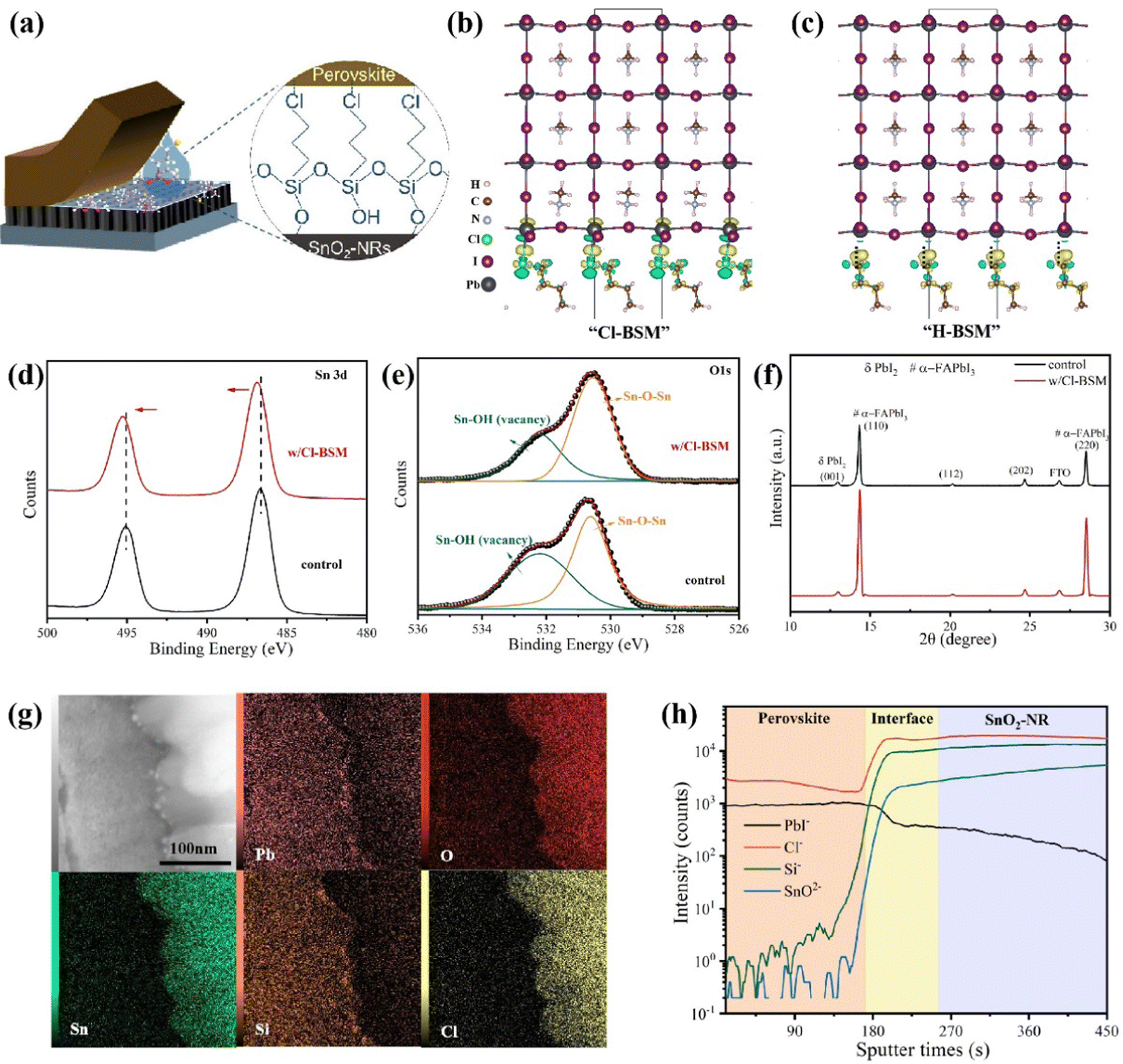 | ||
| Fig. 2 Mechanism study of interpenetrating contact passivation at the SnO2-NRs/Cl-BSM/perovskite interface. (a) Schematic illustration of the mechanism for the SnO2-NRs/Cl-BSM/perovskite interface, and the inset shows a magnified schematic illustration of the formation of Cl-BSM between SnO2-NRs and the perovskite film. (b and c) Charge transfer density difference plots from DFT calculations. Bonding between the PbI2-terminated MAPbI3(001) surface and (b) Cl-BSM or (c) H-BSM. Dashed lines across the interface indicate no bonding. (d and e) High-resolution XPS spectra of SnO2-NRs (control) and SnO2-NRs/Cl-BSM (w/Cl-BSM): (d) Sn 3d core level and (e) O 1s core level. (f) XRD patterns from the top-surfaces of perovskite films based on SnO2-NRs and SnO2-NRs/Cl-BSM. (g) HAADF-STEM cross-sectional image and EDX elemental mapping of perovskite films based on SnO2-NRs/Cl-BSM. (h) ToF-SIMS profiles of the SnO2-NRs/Cl-BSM/perovskite sample. | ||
In order to further explore the surface elements and chemical bonding state of the SnO2-NRs substrate with Cl-BSM deposited, X-ray photoelectron spectroscopy (XPS) measurements are carried out. As shown in Fig. S13 (ESI†), both Si 2p and Cl 2p peaks are located at 102.6 eV and 198.4 eV on the Cl-BSM-coated SnO2-NRs surface (denoted as w/Cl-BSM), but they are absent on the SnO2-NRs surface without a Cl-BSM coating (denoted as control). This demonstrates the successful incorporation of Cl-BSM in the SnO2-NRs substrate. Nevertheless, the binding energy of the Sn 3d core level for the SnO2-NRs/Cl-BSM substrate shows a slight blue chemical shift toward a higher binding energy range in contrast to the control sample as shown in Fig. 2d, demonstrating that an effective chemical interaction formed between SnO2-NRs and Cl-BSM.8Fig. 2e shows the O 1s core level signals from SnO2-NRs with and without Cl-BSM deposition. The peak at 530.3 eV originates from Sn–O–Sn backbones, serving as electron conductance pathways in SnO2-NRs. The signal at a higher binding energy originates from the hydroxyl group (Sn–OH), which acts as a shallow trap site on the surface of SnO2-NRs.55 Importantly, the intensity ratio of Sn–OH to Sn–O–Sn signals is decreased after dipping in Cl-BSM solution, indicating that Sn–O–Si bonds between Cl-BSM and the SnO2-NRs surface may be formed. These results demonstrate that –OH groups are effectively reduced at the SnO2-NRs surface via Sn–O–Si bond formation, which can reduce the concentration of shallow trap sites.
To further explore the crystallization process of the perovskite film based on SnO2-NRs and SnO2-NRs/Cl-BSM, the contact angle measurements were carried out as shown in Fig. S14 (ESI†). Compared with the SnO2-NRs sample with 12.2° as shown in Fig. S3a (ESI†), the SnO2-NRs/Cl-BSM sample exhibits a smaller contact angle of 7.6°. This indicates that SnO2-NRs modified by Cl-BSM show smaller surface Gibbs free energy, thus facilitating the most efficient nucleation process among all perovskite films in this study. In addition, XRD measurement is carried out to characterize the crystallinity of perovskite films based on SnO2-NRs and SnO2-NRs/Cl-BSM substrates. And all the related peaks are defined in Fig. 2f.56,57 Both of the two samples show two strong peaks at about 14.3° and 28.6° as shown in Fig. 2f, which correspond to the (110) and (220) crystal planes of α-FAPbI3, respectively. In addition, the perovskite film based on SnO2-NRs/Cl-BSM exhibits a stronger peak intensity and narrow peak full width at half maximum (FWHM) of the (110) peak than that on the SnO2-NRs substrate, indicating the improvement crystallinity of the perovskite film with the introduction of Cl-BSM into the SnO2-NRs substrate. Besides, the top-view SEM images of perovskite films based on SnO2-NRs and SnO2-NRs/Cl-BSM substrates are shown in Fig. S2a and S15a (ESI†), respectively. Both perovskite crystal images exhibit no obvious difference in the average grain sizes which are 1.13 μm and 1.11 μm, respectively, as shown in Fig. S2c and S16 (ESI†). The cross-sectional SEM image (Fig. S15b, ESI†) shows that the perovskite film based on SnO2-NRs/Cl-BSM exhibits fewer grain boundaries compared with the control sample (Fig. 1b). To further examine the crystallographic orientations of perovskite film based on SnO2-NRs/Cl-BSM, GIWAXS is measured. Compared to the 2D GIWAXS pattern for the control sample on the SnO2-NRs substrate in Fig. 1d, the 2D GIWAXS pattern of the sample on SnO2-NRs/Cl-BSM exhibits higher diffraction (110) and (220) peak intensities at about 10 nm−1 and 20 nm−1 (Fig. S17a, ESI†).44 The integrated intensity profiles along the 10 nm−1 direction for SnO2-NRs/Cl-BSM substrates are also higher than those of SnO2-NRs (Fig. S17b, ESI†). This result indicates a stronger orientational preference with passivation by Cl-BSM. These results indicate that the introduction of Cl-BSM into the SnO2-NRs/perovskite interface can optimize the nucleation of grain growth allowing perovskite film growth more vertically with high crystal quality and improved interfacial contact.
As discussed above, the introduction of Cl-BSM can bridge the SnO2-NRs substrate and the perovskite film via both the halogen bonds and Si–O bonds, which may facilitate the infiltration of the perovskite film into SnO2-NRs and further make a better filling at the SnO2-NRs/perovskite interface. To identify the distribution of Cl-BSM in SnO2-NRs, the HADDF STEM cross-sectional images and EDX cross-sectional elemental mapping images with the architecture of SnO2-NRs/Cl-BSM sample are shown in Fig. S18 (ESI†). It clearly shows that the elements of Si and Cl are mainly located on the upper surface of SnO2-NRs. Similarly, there are still a few Si and Cl elements appearing in the interspace among 1D nanostructured nanorods, indicating that Cl-BSM is successfully deposited on SnO2-NRs. Besides, EDX cross-sectional mapping images displaying the architecture of SnO2-NRs/Cl-BSM/perovskite are further obtained as shown in Fig. 2g. The EDX images clearly disclose the homogeneous distribution of all elements including Pb, O, Sn, Cl and Si in different ranges, consistent with the EDX mapping with the SnO2-NRs/Cl-BSM system in Fig. S18 (ESI†). In addition, Fig. S19 (ESI†) shows the EDX spectrum with the content of various elements at the grain boundary. These results have precisely demonstrated the location of Cl-BSM at the SnO2-NRs/perovskite interface, revealing a mixed element range of Cl-BSM presented with a certain thickness at the SnO2-NRs/perovskite interface. To gain more understanding of the mixed element range at the SnO2-NRs/Cl-BSM/perovskite interface, time-of-flight secondary ion mass spectroscopy (ToF-SIMS) of the SnO2-NRs/Cl-BSM/perovskite system was performed as shown in Fig. 2h. It shows that both the intensities of Cl− and Si− elements are obviously increased across the SnO2-NRs/perovskite interface, and remain stable at the top of SnO2-NRs. Moreover, the X–Z slice and 3D rendering of both Cl− and Si− ToF-SIMS data (Fig. S20, ESI†) clearly display the main distribution of both Cl− and Si− with a certain thickness at the interface between the perovskite layer and SnO2-NRs, which is consistent with the EDX mapping result in Fig. 2g. Besides, there is a plateau of PbI− at the SnO2-NRs/perovskite interface as shown in Fig. 2h, and both the X–Z slice and 3D rendering of PbI− ToF-SIMS data exhibit a certain PbI− thickness at the SnO2-NRs/perovskite interface as shown in Fig. S20 (ESI†). These results indicate that the perovskite film can infiltrate into SnO2-NRs with the introduction of Cl-BSM. As discussed above, both EDX and ToF-SIMS results demonstrate that Cl-BSM has been successfully deposited on the SnO2-NRs substrate, and improved the infiltration of the perovskite at the SnO2-NRs/perovskite interface.
2.3 The defect density and carrier recombination characterization of the perovskite film based on the SnO2-NRs/Cl-BSM substrate
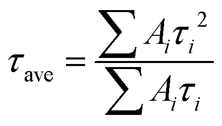
As discussed above, the SnO2-NRs substrate modified by Cl-BSM can make enhanced SnO2-NRs/perovskite interfacial contact, which is expected to effectively extract and transport the charge generated from the perovskite, as well as to reduce the defect concentration at the SnO2-NRs/perovskite interface. The UV-vis transmission spectra of SnO2-NRs with and without Cl-BSM are characterized in Fig. S21 (ESI†). It shows almost the same within the visible light region (400–800 nm), revealing that the introduction of Cl-BSM does not hinder the high transmittance of incident light. Steady-state and time-resolved photoluminescent (PL) spectroscopic techniques are explored to study the charge transfer kinetics across the SnO2-NRs/perovskite interface. Both the intensities of PL based on SnO2-NRs and SnO2-NRs/Cl-BSM are significantly quenched compared with that of the glass substrate as shown in Fig. 3a. However, there is a more distinct quenching in the PL intensity of the device based on the SnO2-NRs/Cl-BSM substrate, which indicates a more efficient electron extraction at the SnO2-NRs/Cl-BSM/perovskite interface. The shallow trap states can be presented at the SnO2-NRs/perovskite interface.23 In particular, the PL peak shows a small blue-shift after the addition of Cl-BSM, indicating the reduction of shallow trap states. In other words, the Cl-BSM can efficiently passivate the trap states at the SnO2-NRs/perovskite interface.58 The TRPL spectra of the perovskite based ETL (Fig. 3b) are recorded to quantify the carrier recombination and the TRPL curve is fitted with a biexponential equation (eqn (1)),47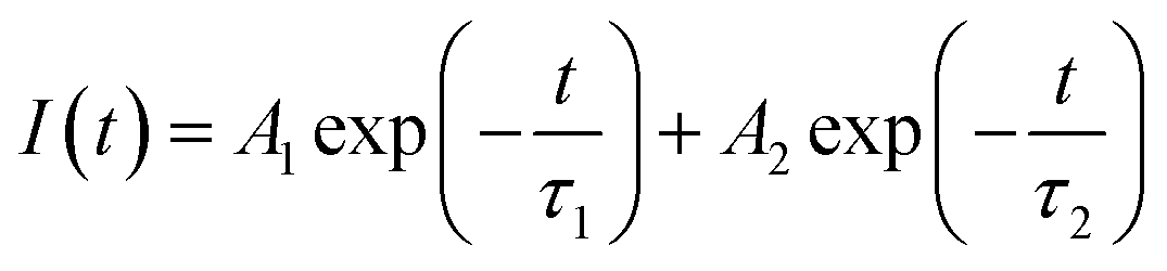 | (1) |
 | (2) |
 | ||
| Fig. 3 The charge transfer between perovskite and different ETLs. (a) PL and (b) steady-state PL spectra of perovskite films at SnO2-NRs and the SnO2-NRs/Cl-BSM ETL. (c) J–V characteristics of the devices FTO/SnO2-NRs/Ag and FTO/SnO2-NRs/Cl-BSM/Ag. (d) The SCLC plots of the electron-only devices displaying VTFL kink point behaviors based on SnO2-NRs and the SnO2-NRs/Cl-BSM ETL. (e) Dark J–V curves of PSCs based on SnO2-NRs and the SnO2-NRs/Cl-BSM ETL. (f) Nyquist plots of PSCs based on the control and with the Cl-BSM deposited SnO2-NRs ETL. | ||
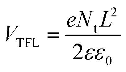
Furthermore, the electrical conductivity of SnO2-NRs and SnO2-NRs/Cl-BSM substrates are measured by current–voltage (J–V) characteristics under dark conditions (Fig. 3c). The devices structured as FTO/SnO2-NRs/Ag and FTO/SnO2-NRs/Cl-BSM/Ag are prepared as shown in the inset of Fig. 3c. It exhibits a higher slope of the SnO2-NRs/Cl-BSM substrate than the control one, indicating the higher electrical conductivity when depositing Cl-BSM on the SnO2-NRs substrate. As reported earlier, the higher conductivity of the ETL substrate can reduce the series resistance and enhance the fill factor of the PSC device.60 The electron trap densities of the perovskite films are quantitatively calculated via space-charge-limited current (SCLC) measurement of electron-only devices as shown in Fig. 3d. It shows three distinct regions, which are n = 1 region with an Ohmic contact, n = 2 region with a Child's law, and n > 3 region with a trap-filled limit, respectively. The trap density Nt can be calculated according to eqn (3),61
 | (3) |
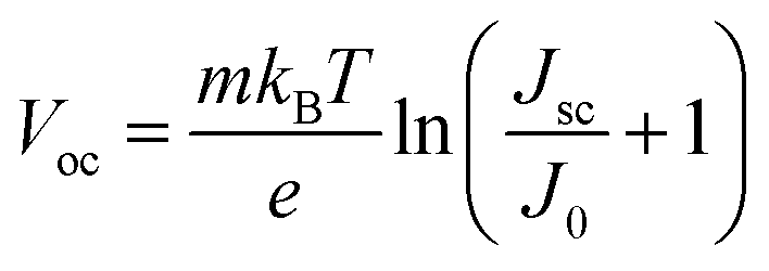
The Voc loss induced by nonradiative recombination is another source to affect the performance of PSCs. To confirm the effect of defect passivation in devices with deposition of Cl-BSM, the J–V characteristics of the devices with and without Cl-BSM are carried out under dark conditions as shown in Fig. 3e. The attainable Voc can be expressed following eqn (4),62
 | (4) |
Furthermore, in order to investigate the electrical properties and charge recombination behavior in the Cl-BSM modified perovskite film, electrochemical impedance spectroscopy (EIS) measurement was carried out as shown in Fig. 3f and the equivalent circuit of PSCs used for fitting impedance data is shown in Fig. S22 (ESI†). The Nyquist plots of PSCs based on SnO2-NRs/Cl-BSM exhibit smaller charge transfer resistance (Rct) compared with the control sample, which should be responsible for the improved FF. In addition, the recombination resistance (Rrec) of PSCs is significantly increased after Cl-BSM modification, revealing the reduced carrier recombination loss in PSCs with decreased defect density.63 Therefore, it is demonstrated that the addition of Cl-BSM can passivate the surface defect states for non-radiative recombination and facilitate the electron extraction at the SnO2-NRs/perovskite interface.
2.4 Photovoltaic performance of PSCs based on SnO2-NRs/Cl-BSM substrate
To further identify the energy band structure of Cl-BSM doping of SnO2-NRs and the perovskite film, ultraviolet photoelectron spectroscopy (UPS) and UV-vis absorption spectroscopy measurements were performed as shown in Fig. S23 and S24 (ESI†). The secondary-electron cutoff binding energies (Ecutoff) of perovskite, SnO2-NRs and SnO2-NRs/Cl-BSM are 17.13 eV, 17.01 eV and 17.09 eV, respectively (Fig. S23, ESI†). The work function (WF) of the films can be calculated by subtracting the Ecutoff from the excitation photon energy of the He I band (21.22 eV), and the values of WF are 4.21 eV for SnO2-NRs, 4.13 eV for SnO2-NRs/Cl-BSM and 4.09 eV for perovskite. Moreover, it is proposed that the structure of the A–O–B interfacial dipole may lead to the reduction of WF, where element A is typically alkali or alkaline earth metal, and element B is usually C or Si.64 Therefore, the decrease of WF may be attributed to the formation of a Sn–O–Si dipole at the ETL/perovskite interface, which can further explain the blue shift of the XPS peak of the Sn element as discussed above. Combining the optical bandgaps derived from both the UV-vis and UPS results, the conduction band minimum (ECB) values of perovskite, SnO2-NRs and Cl-BSM/SnO2-NRs were found to be 3.99 eV, 4.16 eV and 4.03 eV, respectively. It clearly shows that the ECB of the SnO2-NRs/Cl-BSM is closer to the ECB of perovskite than that of the SnO2-NRs ETL. Besides, the energy band diagrams for PSCs incorporating Cl-BSM are illustrated in Fig. 4a, indicating that the device with Cl-BSM exhibits a more favorable band alignment to transfer electrons efficiently. Kelvin probe force microscopy (KPFM) measurement was further carried out to investigate the Cl-BSM effect on the electronic energy levels of SnO2-NRs and perovskite films (Fig. S25, ESI†). It shows that the surface potential of SnO2-NRs/Cl-BSM is higher than that of SnO2-NRs, which is beneficial to transport electrons and suppress carrier recombination.65–67 This result is also consistent with the UPS result. | ||
| Fig. 4 Photovoltaic performance of PSCs based on SnO2-NRs with and without Cl-BSM. (a) Schematic energy level diagram of the perovskite, SnO2-NRs and SnO2-NRs/Cl-BSM. (b) Mott–Schottky plots of PSCs based on SnO2-NRs and SnO2-NRs/Cl-BSM. (c) The champion J–V curves of devices based on SnO2-NRs and SnO2-NRs/Cl-BSM under reverse and forward scans. (d) Statistical box chart of the photovoltaic parameters of the PSCs based on different ETLs. (e) The corresponding EQE spectra along with the integrated Jsc. (f) Steady-state current density and PCE versus time for the champion devices based on SnO2-NRs with and without Cl-BSM. | ||
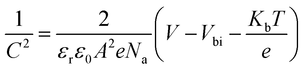
The Mott–Schottky analysis (M–S) is carried out to investigate the influence of carrier transport characteristics in Fig. 4b. The built-in potential (Vbi) of the device is obtained based on M–S analysis using the following equation,68
 | (5) |
As shown in Fig. 4c, the J–V curves of the “champion” PSCs with and without Cl-BSM in reverse scan (RS) and forward scan (FS) are presented, and the corresponding photovoltaic parameters are summarized in Table S5 (ESI†). The champion SnO2-NR based device exhibits PCE values of 19.30% (RS) and 15.64% (FS) with considerable hysteresis (23.4%). Inversely, the SnO2-NRs/Cl-BSM based device shows a negligible J–V hysteresis of 2.6% compared with the reference device as listed in Table S5 (ESI†). Previous research works have reported that hysteresis mainly originates from the existence of traps at the ETL/perovskite interface. Thus, the reduced hysteresis with Cl-BSM can be attributed to the reduced defect concentration and decreased charge accumulation at the SnO2-NRs/Cl-BSM/perovskite interface. The champion SnO2-NRs/Cl-BSM based device exhibits a PCE of 22.42% in RS with Voc = 1.12 V and FF = 81.36%, and a PCE of 21.84% in FS with Voc = 1.12 V and FF = 80.24%, respectively. The improved PCE can be attributed to the increase of Voc from 1.02 V to 1.12 V with decreased charge traps by Cl-BSM addition at the SnO2-NRs/perovskite interface. Besides, the nanostructured SnO2-NRs have large contact areas, which can act as carrier recombination centers and further lead to lower Jsc and decreased FF values, while both the Jsc and FF values of devices passivated by Cl-BSM are higher than that obtained from the control device. The improved Jsc and FF values can be attributed to an effective physical contact of the perovskite film at the ETL/perovskite interface, as well as the improved quality of the perovskite film.
The statistics for the device performance parameters Jsc, Voc, FF and PCE of PSCs (16 of each type) are further presented in Fig. 4d. The reference devices show an average PCE of 18.27% with a Voc of 1 V, Jsc of 24.24 mA cm−2 and FF of 75.32%. However, SnO2-NRs/Cl-BSM ETL based devices exhibit enhanced performance with an average PCE of 21.98%, Voc of 1.11 V, Jsc of 24.49 mA cm−2 and FF of 80.68%. The increased PCE of PSCs based on SnO2-NRs/Cl-BSM can largely be attributed to a slight increase of the FF and, more importantly, the significant improvement of Voc from 1.02 V for the reference device to 1.12 V. Besides, the integrated Jsc values of 24.2 mA cm−2 obtained from the external quantum efficiency (EQE) coincides with the value of Jsc from the J–V curve as shown in Fig. 4e. Steady-state current density and PCE versus time for the champion devices are further monitored at maximum power point (MPP) bias voltages. As illustrated in Fig. 4f, the stabilized PCE values of 22.12% and 18.81% are shown for PSCs based on SnO2-NRs/Cl-BSM and SnO2-NRs ETL after 1000 s, respectively.
As discussed above, the SnO2-NRs modified by Cl-BSM can balance the perovskite film's nucleation/crystal growth process and reduce interfacial defects at the SnO2-NRs/perovskite interface. To further explore the effect of the nucleation process based on SnO2-NRs, the morphological study and device fabrication are also carried out for 2-Me-based antisolvent-free perovskite film deposition on SnO2-NP and SnO2-NRs/Cl-BSM substrates. The J–V curves of PSCs (Fig. S26, ESI†) indicate that an efficiency of 20.77% is achieved for the PSC based on SnO2-NRs/Cl-BSM compared to that of SnO2-NPs (16.26%). Besides, for the SnO2-NP substrate, the surface SEM images show many pinholes with smaller grain sizes (Fig. S27a and S28a, ESI†). On the opposite, for SnO2-NRs/Cl-BSM substrates, the perovskite film exhibits a pinhole-free morphology with an average grain size of 830 nm (Fig. S27b and S28b, ESI†). These results demonstrate that SnO2-NRs can overcome the nucleation barrier of the perovskite film in different solvent systems, which provides a new perspective for researchers to try more host solvents for speeding up the commercialization process of PSCs.
2.5 Operational stability of PSCs based on the SnO2-NRs/Cl-BSM substrate
The currently crucial challenge of PSCs is the limitations of easy degradation and inferior long-term stabilities of perovskite materials, thus inhibiting their future commercial applications. Herein, the operational stability-tested PSCs are investigated after storing the unencapsulated devices under dark ambient conditions with a relative humidity of 25–35% at 20–30 °C. The cross-sectional SEM images of the PSCs based on different ETL substrates after aging for 1000 hours are shown in Fig. 5a. Previous research studies have reported that commercial SnO2-NPs can easily interact with water molecules, and further result in degradation from the underneath of perovskite films.70 As shown in Fig. 5a, the cross-sectional SEM image of the perovskite film based on SnO2-NPs exhibits numerous voids and serious degradation features after aging for 1000 hours. However, the 1D nano-structural SnO2-NRs can protect the integrity of the SnO2-NRs/perovskite interface from moisture penetration due to the large contact surface interaction.71 Besides, compared with the SnO2-NP substrate, the perovskite film based on SnO2-NRs without Cl-BSM modification shows a slightly degraded morphology at SnO2-NRs/perovskite interface. Both the irreversible morphological degradations of the perovskite film based on SnO2-NP and SnO2-NRs may be caused by numerous interfacial defects, which act as carrier recombination centers at the ETL/perovskite interface. In contrast, such degradation features are not seen in the perovskite film based on the SnO2-NRs/Cl-BSM substrate as shown in the cross-sectional SEM image. The aging image of the perovskite film based on SnO2-NRs/Cl-BSM shows a similar morphology to the corresponding fresher SEM image in Fig. 1b. The reduced severity of degradation of the SnO2-NRs/Cl-BSM/perovskite interface can be attributed to the following effects of the Cl-BSM. Firstly, the introduction of Cl-BSM has reduced the prevalence of –OH groups at the SnO2-NRs surface, effectively suppressing the interfacial shallow trap sites, which can serve as sites for photocarrier recombination. Secondly, the Cl-termination molecule can effectively passivate the interfacial defect states between SnO2-NRs and the perovskite film, thus decreasing the charge accumulation and reducing non-radiative recombination at the SnO2-NRs/Cl-BSM/perovskite interface. | ||
| Fig. 5 Characterization of operational stability-tested PSCs. (a) Cross-sectional SEM images of the PSCs based on different ETL tested for 1000 hours under dark ambient conditions with a relative humidity of 25–35% at 20–30 °C. (b) Stability tests of unsealed cells with different ETL under simulated solar light (AM 1.5, 100 mW cm−2, N2 glovebox). (c) Shelf life of the unencapsulated PSCs with different ETL stored under ambient air (relative humidity of 25–35% at 20–30 °C). | ||
With light radiation, the perovskite film is prone to phase segregation or chemical decomposition, and the ETL tend to introduce new defects at the ETL/perovskite interface.72 Therefore, the light stability under continuous irradiation simulated solar light (AM 1.5, 100 mW cm−2, N2) and long-term stability (ambient dark, 25–35% RH) of unsealed devices based on SnO2-NRs or SnO2-NRs/Cl-BSM substrates are further evaluated (Fig. 5b and c). The PSCs based on SnO2-NRs/Cl-BSM remain about 91% of its champion PCE after 500 hours of continuous irradiation as shown in Fig. 5b. Inversely, the reference PSCs decreased to 77% of its origin PCE indicating the instability under the continuous irradiation. As discussed above, the unsealed PSCs based on SnO2-NRs/Cl-BSM with improved light-stability can be attributed to the decreased defect sites on the SnO2-NRs surface. Meanwhile, Fig. 5c shows the 1000 hours shelf life tested with unencapsulated devices under ambient conditions at 25–35% relative humidity and 20–30 °C. The target PSCs retained 85% of the maximum PCE (22.42%) after 1000 hours of storage, whereas the SnO2-NRs based PSCs decreased to almost 56% of the initial PCE. The improved moisture stability of PSCs stored at a relative humidity of 25–35% in the dark can be attributed to the strengthened SnO2-NRs/Cl-BSM/perovskite interface and the decreased defect accumulation at the interface. As a result, the unencapsulated PSCs based on the SnO2-NRs/Cl-BSM ETL have long-term optimal stability properties than the reference device. These results indicate that the introduction of Cl-BSM not only stabilizes the SnO2-NRs/perovskite interface under continues irradiation, but also improves the overall resistance against moisture penetration under ambient conditions.
3. Conclusion
In conclusion, this work demonstrates a green-solvent-deposited formamidinium-based perovskite film based on the SnO2-NRs substrate with Cl-terminated bifunctional supramolecule (Cl-BSM) passivation. Through the SnO2-NRs substrate, fast heterogeneous nucleation and retarded crystal growth can be achieved to facilitate the uniform grain growth of the perovskite film deposited from the green solvent as well as the antisolvent-free system. To overcome the severe interfacial recombination that is commonly seen in the NRs-substrate due to the vast contact area, Cl-BSM is introduced. The characterization and analysis show that the introduction of Cl-BSM between SnO2-NRs and the perovskite film can resurrect the defective interface and strengthen interfacial contact. Moreover, the –Si(OCH3)3 group of Cl-BSM can form Si–O bonds with SnO2-NRs for reducing the prevalence of –OH groups at the SnO2-NRs surface, further stabilizing the SnO2-NRs/perovskite interface. Meanwhile, the DFT and experimental evidence suggest that the Cl-terminal group of Cl-BSM has strong anchoring with the perovskite surface by halogen bonds (Pb–Cl), leading to a strong contact interface and decreased defect concentration at the SnO2-NRs/perovskite interface. As a result, a champion efficiency of 22.42% is demonstrated by utilizing both SnO2-NRs and Cl-BSM as substrates. Furthermore, the presence of Cl-BSM can avoid interfacial voids and delamination that occur during the aging test. Correspondingly, the improved operation stability can retain 91% and 85% of the maximum PCE after 500 hours of continuous irradiation and after 1000 hours of ambient storage, respectively.4. Experimental section
Materials
Fluorine-doped tin oxide (FTO) glass substrates (sheet resistance 10 Ω sq−1) were purchased from Liaoning Huite Optoelectronics Technology Co., Ltd. The SnO2 colloid precursor (tin(IV) oxide, 15% in H2O colloidal dispersion) was obtained from Alfa Aesar. SnCl2·2H2O (99.99%), SnCl4·5H2O (99.995%), triethyl phosphate (TEP, 99%), dibutyl ether (DEE, 99.7%), 2-methoxyethanol (2-Me, 99.8%), chlorobenzene (CB, 99.9%), 4-tert-butylpyridine (t-BP, 96%) and (3-chloropropyl)trimethoxysilane (Si(OCH3)3(CH2)3H, 98%) were obtained from Sigma Aldrich. Ethanol (95%), isopropanol (IPA, 99.8%) and concentrated HCl (36.5–38 wt%, GR) were purchased from Aladdin Biochemical Technology Co., Ltd. Lead(II) iodide (PbI2, 99.99%), formamidine iodide (FAI, 99.5%), lead(II) bromide (PbBr2, 99.5%), methylammonium chloride (MACl, 99.5%), methylammonium bromide (MABr, 99.5%), n-butylamine hydrochloride (BACl, 98%), 2,2′,7,7′-tetrakis-(N,N-di-p-methoxyphenylamine)-9,9′-spirobifluorene (spiro-OMeTAD, 99%) and lithium bis(trifluoromethylsulfonyl)imide (Li-TFSI, 95%) were purchased from Xi’an Polymer Light Technology. All materials are used directly without any further purification.Synthesis of 1D nanostructured SnO2 nanorod arrays
FTO substrates are pre-washed sequentially using ethanol, detergent solution, deionized water, acetone and IPA in an ultrasonic bath, for 15 min each. After drying with N2 flow, the FTO substrates are treated with UV-ozone for 20 min. Then, a compact seed layer is spin-coated on the FTO substrates at 1000 rpm for 10 s and 4000 rpm for 30 s, and annealed at 500 °C for 30 min in ambient air. To prepare the seed solution, 10 mL of SnCl2·2H2O (225.65 mg) isopropanol solution is refluxed at 70 °C for one hour.The 1D nanostructured SnO2 nanorods are grown on the FTO substrates coated with a seed layer via the hydrothermal method. A teflon-lined stainless-steel autoclave (100 mL) contains 25 mL of ethanol and 25 mL of ultrapure water with 4 mM SnCl4·5H2O, and then 2 mL of concentrated HCl were added slowly and the mixture solution was stirred under ambient conditions for 20 min to obtain a transparent solution. The FTO substrates have been placed against the wall with the seed layer side facing down. The SnO2-NRs with various morphologies are obtained at different reaction temperatures for 12 h at 180, 200 and 220 °C. The autoclaves are cooled down to room temperature naturally, and the FTO/SnO2-NR substrates are rinsed extensively with ultrapure water and ethanol. Finally, the FTO/SnO2-NR substrates are annealed at 500 °C for 30 min in air. Modified with Cl-BSM, the as-fabricated FTO/SnO2-NR substrates are submerged in a 0.1 M solution of Si(OCH3)3(CH2)3H in isopropanol/ultrapure water (v/v = 95/5) for 1 h. Subsequently, the substrates are further rinsed with isopropanol several times, and then dried under flowing dry N2 and annealed at 100 °C for 5 min.
Device fabrication
FTO substrates are sequentially cleaned using ethanol, detergent solution, deionized water, acetone and IPA in an ultrasonic bath for 15 min, dried with N2 flow, and then treated with UV-ozone for 20 min before deposition of functional layers. The electron transport layer of SnO2-NRs is prepared by following the method of 1D nanostructured SnO2 nanorod arrays. The 3.75 wt% SnO2 colloidal solution was used by diluting 15 wt% SnO2 colloidal solution with deionized water. SnO2 colloidal solution is spin-coated on FTO substrates at 3000 rpm for 30 s and annealed at 160 °C for 30 min in ambient air. Before deposition of perovskite films in a N2-filled glovebox, all substrates are treated in a UV-ozone cleaner for 10 min. The preparation process of the green-solvent-based perovskite films is illustrated as shown in Fig. 1a. 70 μL (FAPbI3)0.95(MAPbBr3)0.05 precursor solution (1.3 M) with 5 mol% excess PbI2 and 45 mol% excess MACl is spin-coated on SnO2-coated substrates at 3000 rpm for 10 s and 4000 rpm for 30 s. 100 μL of anti-solvent DEE is dropped at the center of FTO/SnO2-NR substrates at the 29th second of the spinning process. Subsequently, the intermediate phase films are annealed at 150 °C for 10 min. For antisolvent-free deposition, 40 mol% MACl and 10 mol% n-butylamine (BACl) is mixed with 1.3 M FAPbI3 in 1 mL of 2-Me. Besides, 70 μL FAPbI3 is spin-coated on SnO2-coated substrates at 1000 rpm for 3 s and 6000 rpm for 20 s and annealed at 150 °C for 15 min. The spiro-OMeTAD solution is prepared by dissolving 72.3 mg of spiro-OMeTAD with additives in 1 mL of CB. 17.5 μL of Li-TFSI solution (520 mg mL−1 in acetonitrile) and 22.5 μL of t-BP were added to the solution. The spiro-OMeTAD hole transport layer (HTL) is prepared by spin-coating the solution at 3000 rpm for 30 s. Both perovskite and HTL deposition is performed in a N2-filled glovebox. Finally, 100 nm of Ag layer is thermally-evaporated on top of the HTL as an electrode. The Spiro-OMeTAD is changed to PTAA for stability test.Characterization
The current density–voltage (J–V) curves of the devices were measured under AM1.5G illumination at 100 mW cm−2 using an Abet Technologies Sun 2000 solar simulator. The intensity was calibrated using a standard VLSI Si reference solar cell (SRC-1000-TC-K-QZ). The device was measured by reverse scan ranging from 1.2 V to −0.1 V with an interval of 50 mV s−1, and forward scan ranging from −0.1 V to 1.2 V with an interval of 50 mV s−1 in ambient air (30% RH). The active device area of PSCs during the measurements is 0.168 cm2 defined by a metal mask with an aperture area of 0.1 cm2 when we measured the solar cells. External quantum efficiency (EQE) spectra were recorded on a QTEST HIFINITY 5 EQE system (the light intensity was calibrated with standard Si detectors) in air. Electrochemical impedance spectroscopy (EIS) spectra were recorded using a Chenhua CHI660E electrochemical workstation under a dark environment with a bias potential of 0.6 V. Space-charge-limited current (SCLC) characteristics of the electron-only transport devices were measured using a Keithley 2400 with a scan step 0.01 V.The transmittance and absorbance spectra were recorded with a UV-vis-NIR spectrometer (Lambda 1050, PerkinElmer) installed with a 150 mm integrating sphere. Steady state photoluminescence (PL) spectra and time-resolved photoluminescence (TRPL) spectra were recorded on an FLS 1000 photoluminescence spectrometer with an excitation wavelength of 465 nm. X-Ray diffraction (XRD) patterns were obtained with a D8 Advance X-ray diffractometer with Cu Kα radiation as the X-ray source at a scan rate of 6° min−1. X-Ray photoelectron spectra (XPS) analysis was carried out using a Thermo Scientific K-Alpha X-ray photoelectron spectrometer and calibrated with C1s binding energy. Ultraviolet photoelectron spectra (UPS) were recorded using a photoelectron spectroscopy system (AXIS Ultra DLD) under excitation from the He I line (21.22 eV) of a helium discharge lamp. The time-of-flight secondary-ion mass spectrometry (ToF-SIMS) measurements were analyzed in dual beam profiling mode on a ToF-SIMS 5-100, including the primary ion (30k eV Bi3+) and the sputter ion (5k eV Ar-cluster). Contact angles were measured using a DSA100 instrument. GIWAXS experiments were performed at beamline BL14B in the Shanghai Synchrotron Radiation Facility (SSRF) with an X-ray wavelength of 0.124 nm. Field emission scanning electron microscopy (FESEM) images were acquired on a JSM-7800F FE-SEM. The microstructure and composition of the samples were characterized with a JEOL ARM200F transmission electron microscope, which was operated at an acceleration voltage of 200 kV, and equipped with an energy dispersive X-ray (EDX) spectroscopy detector.
Method for preparing cross-sectional STEM samples
Cross-sectional scanning TEM (STEM) samples were prepared using a multi-Beam SEM-FIB nanofabrication platform (JEOL-Model JIB-4501). To protect the surface from damage during FIB milling, the cross-sectional surface was in situ-deposited with platinum (Pt) using a gallium ion beam and then milled to less than 100 nm thick lamella gradually. The architecture of the Cl-BSM/SnO2-NRs sample was Pt/SnO2-NRs/Cl-BSM/FTO, which was ex situ lifted out to the Quantifoil holey carbon Cu grid lift-off FIB technique. We prepared the PSC sample with the architecture of Pt/Ag/SnO2-NRs/Cl-BSM/FTO using an FIB workstation.First principles density functional theory calculations
Owing to the unlikely influence of the Si-based anchor group on the bonding at the other end of the alkyl chains, this work uses the aligned butane [H(CH2)4H] and Cl-terminated butane [H(CH2)4Cl] molecules to represent [Si(OCH3)3(CH2)3H] (denoted as H-BSM) and [Si(OCH3)3(CH2)3Cl] (denoted as Cl-BSM), respectively. The present first principles density functional theory (DFT) calculations are performed using the Vienna Ab initio Simulation Package (VASP) by the projector augmented wave (PAW) method. The generalized gradient approximation (GGA) of the Perdew–Burke–Ernzerhof (PBE) exchange-functional and an energy cutoff of 500 eV were employed. The force on each atom less than 0.02 eV Å−1 is set for the convergence criterion of geometry relaxation. 4 × 4 × 4 and 4 × 4 × 1 Γ-centered grids of k-points are applied for bulk and slab calculations, respectively. The self-consistent calculations apply a convergence energy threshold of 10−5 eV. A 1 × 1 simulation cell with either 7 (PbI2-terminated) or 8 (MAI-terminated) atomic layers along with an at least 25 Å thick vacuum layer normal to the (001) plane constitute the slab model. The adhesion property is measured by the work of separation (Wsep), which is defined as the energy difference between the fully optimized interface (Ei(DFT)) and the unoptimized separated (r ∼ 8 Å) interface structures (Er=8 (DFT)), and further divided by the interface area (A):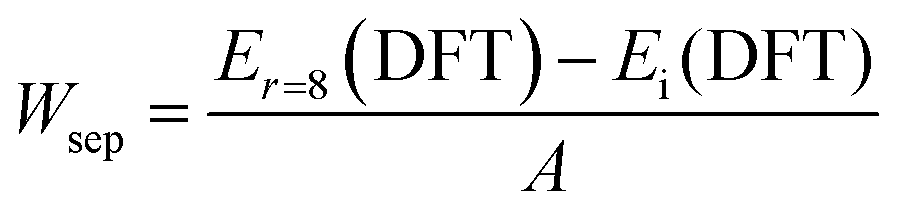
Conflicts of interest
The authors declare no conflicts of interest.Acknowledgements
This study was funded by the National Natural Science Foundation of China (grant no. 52150610487, 51850410501 and 51950410581), the Natural Science Foundation of Shanghai (22ZR1428200), the Shanghai Government (20JC141500), and CATL-SJTU joint funding. We acknowledged the support from staff at beamline BL16B1 in the Shanghai Synchrotron Radiation Facility (SSRF) for the GIWAXS measurement. We acknowledged the Instrumental Analysis Center of Shanghai Jiao Tong University for providing SEM, UPS, XPS and TOF-SIMS measurements.References
- X. Wang, Y. Qiu, L. Wang, T. Zhang, L. Zhu, T. Shan, Y. Wang, J. Jiang, L. Kong, H. Zhong, H. Yu, F. Liu, F. Gao, F. Wang and C.-C. Chen, Nano Energy, 2021, 89, 106445 CrossRef CAS.
- M. A. Green, A. Ho-Baillie and H. J. Snaith, Nat. Photonics, 2014, 8, 506–514 CrossRef CAS.
- Y. Li, Z. Shi, W. Liang, J. Ma, X. Chen, D. Wu, Y. Tian, X. Li, C. Shan and X. Fang, Mater. Horiz., 2021, 8, 1367–1389 RSC.
- H. Min, D. Y. Lee, J. Kim, G. Kim, K. S. Lee, J. Kim, M. J. Paik, Y. K. Kim, K. S. Kim, M. G. Kim, T. J. Shin and S. II Seok, Nature, 2021, 598, 444–450 CrossRef CAS PubMed.
- Z. Li, M. Yang, J.-S. Park, S.-H. Wei, J. J. Berry and K. Zhu, Chem. Mater., 2015, 28, 284–292 CrossRef.
- J. J. Yoo, G. Seo, M. R. Chua, T. G. Park, Y. Lu, F. Rotermund, Y. K. Kim, C. S. Moon, N. J. Jeon, J. P. Correa-Baena, V. Bulovic, S. S. Shin, M. G. Bawendi and J. Seo, Nature, 2021, 590, 587–593 CrossRef CAS.
- Q. Dong, C. Zhu, M. Chen, C. Jiang, J. Guo, Y. Feng, Z. Dai, S. K. Yadavalli, M. Hu, X. Cao, Y. Li, Y. Huang, Z. Liu, Y. Shi, L. Wang, N. P. Padture and Y. Zhou, Nat. Commun., 2021, 12, 973 CrossRef CAS PubMed.
- H. Xu, Y. Miao, N. Wei, H. Chen, Z. Qin, X. Liu, X. Wang, Y. Qi, T. Zhang and Y. Zhao, Adv. Energy Mater., 2021, 12, 2103151 CrossRef.
- L. Wang, X. Wang, L.-L. Deng, S. Leng, X. Guo, C.-H. Tan, W. C. H. Choy and C.-C. Chen, Mater. Horiz., 2020, 7, 934–942 RSC.
- H. B. Lee, M. K. Jeon, N. Kumar, B. Tyagi and J. W. Kang, Adv. Funct. Mater., 2019, 29, 1903213 CrossRef.
- M. Yavari, M. Mazloum-Ardakani, S. Gholipour, M. M. Tavakoli, S.-H. Turren-Cruz, N. Taghavinia, M. Grätzel, A. Hagfeldt and M. Saliba, Adv. Energy Mater., 2018, 8, 1800177 CrossRef.
- Y. Yun, F. Wang, H. Huang, Y. Fang, S. Liu, W. Huang, Z. Cheng, Y. Liu, Y. Cao, M. Gao, L. Zhu, L. Wang, T. Qin and W. Huang, Adv. Mater., 2020, 32, e1907123 CrossRef.
- M. Wang, Q. Fu, L. Yan, J. Huang, Q. Ma, M. Humayun, W. Pi, X. Chen, Z. Zheng and W. Luo, Chem. Eng. J., 2020, 387, 123966 CrossRef CAS.
- W. Xu, Y. Gao, W. Ming, F. He, J. Li, X. H. Zhu, F. Kang, J. Li and G. Wei, Adv. Mater., 2020, 32, e2003965 CrossRef PubMed.
- D.-K. Lee, K.-S. Lim, J.-W. Lee and N.-G. Park, J. Mater. Chem. A, 2021, 9, 3018–3028 RSC.
- T. Bu, L. K. Ono, J. Li, J. Su, G. Tong, W. Zhang, Y. Liu, J. Zhang, J. Chang, S. Kazaoui, F. Huang, Y.-B. Cheng and Y. Qi, Nat. Energy, 2022, 7, 528–536 CrossRef CAS.
- S. Shan, Y. Li, H. Wu, T. Chen, B. Niu, Y. Zhang, D. Wang, C. Kan, X. Yu, L. Zuo and H. Chen, SusMat, 2021, 1, 537–544 CrossRef.
- J. Küffner, J. Hanisch, T. Wahl, J. Zillner, E. Ahlswede and M. Powalla, ACS Appl. Energy Mater., 2021, 4, 11700–11710 CrossRef.
- S. H. Huang, K. Y. Tian, H. C. Huang, C. F. Li, W. C. Chu, K. M. Lee, Y. C. Huang and W. F. Su, ACS Appl. Mater. Interfaces, 2020, 12, 26041–26049 CrossRef CAS.
- M. Wang, C. Fei, M. A. Uddin and J. Huang, Sci. Adv., 2022, 8, eabo5977 CrossRef PubMed.
- K. H. Hendriks, J. J. van Franeker, B. J. Bruijnaers, J. A. Anta, M. M. Wienk and R. A. J. Janssen, J. Mater. Chem. A, 2017, 5, 2346–2354 RSC.
- Y. Deng, C. H. Van Brackle, X. Dai, J. Zhao, B. Chen and J. Huang, Sci. Adv., 2019, 5, eaax7537 CrossRef CAS.
- S. H. Lee, S. Hong and H. J. Kim, ACS Appl. Mater. Interfaces, 2022, 14, 39132–39140 CrossRef CAS.
- J. W. Yoo, J. Jang, U. Kim, Y. Lee, S. G. Ji, E. Noh, S. T. Hong, M. Choi and S. II Seok, Joule, 2021, 5, 2420–2436 CrossRef CAS.
- L. Guo, Y. Chen, G. Wang, Y. Xia, D. Luo, Z. Zhu, C. Wang, W. Dong and S. Wen, ACS Appl. Energy Mater., 2021, 4, 2681–2689 CrossRef CAS.
- Q. Zhang, G. Ma, K. A. Green, K. Gollinger, J. Moore, T. Demeritte, P. C. Ray, G. A. Hill, X. Gu, S. E. Morgan, M. Feng, S. Banerjee and Q. Dai, ACS Appl. Energy Mater., 2022, 5, 1487–1495 CrossRef CAS.
- X. Cao, L. Hao, Z. Liu, G. Su, X. He, Q. Zeng and J. Wei, Chem. Eng. J., 2022, 437, 135458 CrossRef CAS.
- Y. Yun, D. Vidyasagar, M. Lee, O. Y. Gong, J. Jung, H. S. Jung, D. H. Kim and S. Lee, Adv. Sci., 2021, 8, e2102492 CrossRef PubMed.
- K. Wang, C. Wu, Y. Hou, D. Yang, T. Ye, J. Yoon, M. Sanghadasa and S. Priya, Energy Environ. Sci., 2020, 13, 3412–3422 RSC.
- H. Zhang, K. Darabi, N. Y. Nia, A. Krishna, P. Ahlawat, B. Guo, M. H. S. Almalki, T. S. Su, D. Ren, V. Bolnykh, L. A. Castriotta, M. Zendehdel, L. Pan, S. S. Alonso, R. Li, S. M. Zakeeruddin, A. Hagfeldt, U. Rothlisberger, A. Di Carlo, A. Amassian and M. Gratzel, Nat. Commun., 2022, 13, 89 CrossRef CAS PubMed.
- F. Huang, A. R. Pascoe, W. Q. Wu, Z. Ku, Y. Peng, J. Zhong, R. A. Caruso and Y. B. Cheng, Adv. Mater., 2017, 29, 1601715 CrossRef.
- A. R. Pascoe, S. Meyer, W. Huang, W. Li, I. Benesperi, N. W. Duffy, L. Spiccia, U. Bach and Y.-B. Cheng, Adv. Funct. Mater., 2016, 26, 1278–1285 CrossRef CAS.
- J. Choi, S. Song, M. T. Horantner, H. J. Snaith and T. Park, ACS Nano, 2016, 10, 6029–6036 CrossRef CAS.
- G. Li, J. Song, C. Meng, D. Wang, Z. Du, W. Sun, J. Wu and Z. Lan, Solar RRL, 2020, 4, 2000519 CrossRef CAS.
- G. Li, K. Deng, Y. Dou, Y. Liao, D. Wang, J. Wu and Z. Lan, Sol. Energy, 2019, 193, 111–117 CrossRef CAS.
- C. Zhang, X. Deng, J. Zheng, X. Zhou, J. Shi, X. Chen, Z. Sun and S. Huang, Electrochim. Acta, 2018, 283, 1134–1145 CrossRef CAS.
- H. Sun, K. Deng, Y. Zhu, M. Liao, J. Xiong, Y. Li and L. Li, Adv. Mater., 2018, 30, e1801935 CrossRef PubMed.
- C. Gao, S. Yuan, B. Cao and J. Yu, Chem. Eng. J., 2017, 325, 378–385 CrossRef CAS.
- X. Zhang, Y. Rui, Y. Wang, J. Xu, H. Wang, Q. Zhang and P. Müller-Buschbaum, J. Power Sources, 2018, 402, 460–467 CrossRef CAS.
- D. Zhong, B. Cai, X. Wang, Z. Yang, Y. Xing, S. Miao, W.-H. Zhang and C. Li, Nano Energy, 2015, 11, 409–418 CrossRef CAS.
- Y. Lv, R. Yuan, B. Cai, B. Bahrami, A. H. Chowdhury, C. Yang, Y. Wu, Q. Qiao, S. F. Liu and W. H. Zhang, Angew. Chem. Int. Ed. Engl., 2020, 59, 11969–11976 CrossRef CAS PubMed.
- F. Wang, M. Yang, Y. Zhang, L. Yang, L. Fan, S. Lv, X. Liu, D. Han and J. Yang, Adv. Sci., 2019, 6, 1801170 CrossRef.
- D. Yang, R. Yang, K. Wang, C. Wu, X. Zhu, J. Feng, X. Ren, G. Fang, S. Priya and S. F. Liu, Nat. Commun., 2018, 9, 3239 CrossRef PubMed.
- H. Hu, Z. Ren, P. W. K. Fong, M. Qin, D. Liu, D. Lei, X. Lu and G. Li, Adv. Funct. Mater., 2019, 29, 1900092 CrossRef.
- Y. Yang, J. Wu, X. Wang, Q. Guo, X. Liu, W. Sun, Y. Wei, Y. Huang, Z. Lan, M. Huang, J. Lin, H. Chen and Z. Wei, Adv. Mater., 2020, 32, e1904347 CrossRef.
- H. Denny Kamaruddin, J. Membr. Sci., 1997, 135, 147–159 CrossRef.
- J. Yang, W. Tang, R. Yuan, Y. Chen, J. Wang, Y. Wu, W. J. Yin, N. Yuan, J. Ding and W. H. Zhang, Chem. Sci., 2020, 12, 2050–2059 RSC.
- H. Sun, K. Deng, Y. Zhu, M. Liao, J. Xiong, Y. Li and L. Li, Adv. Mater., 2018, 30, 1801935 CrossRef.
- W.-Q. Wu, F. Huang, D. Chen, Y.-B. Cheng and R. A. Caruso, Adv. Funct. Mater., 2015, 25, 3264–3272 CrossRef CAS.
- L. Vayssieres and M. Graetzel, Angew. Chem., 2004, 116, 3752–3756 CrossRef.
- S. D. Stranks, G. E. Eperon, G. Grancini, C. Menelaou, M. J. Alcocer, T. Leijtens, L. M. Herz, A. Petrozza and H. J. Snaith, Science, 2013, 342, 341–344 CrossRef CAS.
- L. Canil, J. Salunke, Q. Wang, M. Liu, H. Köbler, M. Flatken, L. Gregori, D. Meggiolaro, D. Ricciarelli, F. De Angelis, M. Stolterfoht, D. Neher, A. Priimagi, P. Vivo and A. Abate, Adv. Energy Mater., 2021, 11, 2101553 CrossRef CAS.
- G. Cavallo, P. Metrangolo, R. Milani, T. Pilati, A. Priimagi, G. Resnati and G. Terraneo, Chem. Rev., 2016, 116, 2478–2601 CrossRef CAS PubMed.
- Z. Dai, S. K. Yadavalli, M. Chen, A. Abbaspourtamijani, Y. Qi and N. P. Padture, Science, 2021, 372, 618–622 CrossRef CAS.
- Z. Xiong, X. Chen, B. Zhang, G. O. Odunmbaku, Z. Ou, B. Guo, K. Yang, Z. Kan, S. Lu, S. Chen, N. A. N. Ouedraogo, Y. Cho, C. Yang, J. Chen and K. Sun, Adv. Mater., 2022, 34, e2106118 CrossRef.
- J. Fang, Z. Ding, X. Chang, J. Lu, T. Yang, J. Wen, Y. Fan, Y. Zhang, T. Luo, Y. Chen, S. Liu and K. Zhao, J. Mater. Chem. A, 2021, 9, 13297–13305 RSC.
- C. C. Zhang, S. Yuan, Y. H. Lou, Q. W. Liu, M. Li, H. Okada and Z. K. Wang, Adv. Mater., 2020, 32, e2001479 CrossRef.
- T. Bu, J. Li, F. Zheng, W. Chen, X. Wen, Z. Ku, Y. Peng, J. Zhong, Y. B. Cheng and F. Huang, Nat. Commun., 2018, 9, 4609 CrossRef PubMed.
- J. Liang, Z. Zhang, Q. Xue, Y. Zheng, X. Wu, Y. Huang, X. Wang, C. Qin, Z. Chen and C.-C. Chen, Energy Environ. Sci., 2022, 15, 296–310 RSC.
- Z. Li, Z. Wang, C. Jia, Z. Wan, C. Zhi, C. Li, M. Zhang, C. Zhang and Z. Li, Nano Energy, 2022, 94, 106919 CrossRef CAS.
- Z. Zhang, J. Jiang, X. Xiao Liu, X. Wang, L. Wang, Y. Qiu, Z. Zhang, Y. Zheng, X. Wu, J. Liang, C. Tian and C. C. Chen, Small, 2022, 18, e2105184 CrossRef.
- T. He, S. Li, Y. Jiang, C. Qin, M. Cui, L. Qiao, H. Xu, J. Yang, R. Long, H. Wang and M. Yuan, Nat. Commun., 2020, 11, 1672 CrossRef CAS PubMed.
- X. Liu, Z. Zhang, J. Jiang, C. Tian, X. Wang, L. Wang, Z. Zhang, X. Wu, Y. Zheng, J. Liang and C.-C. Chen, Chem. Eng. J., 2022, 432, 134382 CrossRef CAS.
- J. Huang, Z. Xu and Y. Yang, Adv. Funct. Mater., 2007, 17, 1966–1973 CrossRef CAS.
- P. Cui, D. Wei, J. Ji, H. Huang, E. Jia, S. Dou, T. Wang, W. Wang and M. Li, Nat. Energy, 2019, 4, 150–159 CrossRef CAS.
- H. Dong, S. Pang, Y. Xu, Z. Li, Z. Zhang, W. Zhu, D. Chen, H. Xi, Z. Lin, J. Zhang, Y. Hao and C. Zhang, ACS Appl. Mater. Interfaces, 2020, 12, 54703–54710 CrossRef CAS.
- W. Z. Li, W. Zhang, S. Van Reenen, R. J. Sutton, J. D. Fan, A. A. Haghighirad, M. B. Johnston, L. D. Wang and H. J. Snaith, Energy Environ. Sci., 2016, 9, 490–498 RSC.
- Y. Zheng, X. Wu, J. Liang, Z. Zhang, J. Jiang, J. Wang, Y. Huang, C. Tian, L. Wang, Z. Chen and C. C. Chen, Adv. Funct. Mater., 2022, 32, 2200431 CrossRef CAS.
- L. Zhu, X. Zhang, M. Li, X. Shang, K. Lei, B. Zhang, C. Chen, S. Zheng, H. Song and J. Chen, Adv. Energy Mater., 2021, 11, 2100529 CrossRef CAS.
- S. Ullah, M. F. U. Din, J. Khan Kasi, A. Khan Kasi, K. Vegso, M. Kotlar, M. Micusik, M. Jergel, V. Nadazdy, P. Siffalovic, E. Majkova and A. Fakharuddin, ACS Appl. Nano Mater., 2022, 5, 7822–7830 CrossRef CAS.
- B. Roose, J.-P. C. Baena, K. C. Gödel, M. Graetzel, A. Hagfeldt, U. Steiner and A. Abate, Nano Energy, 2016, 30, 517–522 CrossRef CAS.
- J. Wei, Q. Wang, J. Huo, F. Gao, Z. Gan, Q. Zhao and H. Li, Adv. Energy Mater., 2020, 11, 2002326 CrossRef.
Footnote |
| † Electronic supplementary information (ESI) available. See DOI: https://doi.org/10.1039/d2mh00970f |
| This journal is © The Royal Society of Chemistry 2023 |