
 Open Access Article
 This Open Access Article is licensed under a Creative Commons Attribution-Non Commercial 3.0 Unported Licence
Influence of alkali iodide fluxes on Cu2ZnSnS4 monograin powder properties and performance of solar cells
Kristi
Timmo
 *a,
Maris
Pilvet
a,
Katri
Muska
a,
Mare
Altosaar
a,
Valdek
Mikli
a,
Reelika
Kaupmees
a,
Raavo
Josepson
b,
Jüri
Krustok
a,
Maarja
Grossberg-Kuusk
a and
Marit
Kauk-Kuusik
a
*a,
Maris
Pilvet
a,
Katri
Muska
a,
Mare
Altosaar
a,
Valdek
Mikli
a,
Reelika
Kaupmees
a,
Raavo
Josepson
b,
Jüri
Krustok
a,
Maarja
Grossberg-Kuusk
a and
Marit
Kauk-Kuusik
a
aDepartment of Materials and Environmental Technology, Tallinn University of Technology, Ehitajate tee 5, 19086 Tallinn, Estonia. E-mail: kristi.timmo@taltech.ee
bDivision of Physics, Tallinn University of Technology, Ehitajate tee 5, 19086 Tallinn, Estonia
First published on 5th September 2023
Abstract
One promising and cost-effective method to produce flexible solar panels in the future is monograin layer (MGL) solar cell technology based on monograin powder (MGP) crystals. The results of the present study demonstrate the influence of different alkali salts (LiI, NaI, KI, RbI and CsI) on the properties of Cu2ZnSnS4 (CZTS) MGPs and their effect on the characteristics of MGL solar cells. SEM and EDX studies revealed that the morphology and composition of the formed crystals are influenced by the nature of the flux materials. Structural studies by XRD showed good crystallinities for all MGPs. However, CZTS crystals grown in LiI exhibited a shift of all diffraction peaks towards lower angles and larger lattice parameter values. In addition, powder grown in LiI exhibited the broadest main Raman peak (FWHM = 7.06 cm−1). When CsI was used, the Raman peaks were sharper and narrower with FWHM of 4.5 cm−1, showing a higher level of crystallinity compared to other produced powders. The estimated band gap energy values obtained from EQE measurements were ∼1.57 eV for NaI, KI, RbI, CsI and 1.65 eV for LiI grown CZTS MGPs. The analysis of temperature-dependent current–voltage characteristics indicated that tunneling enhanced interface recombination is the prevailing process in all materials. At low temperatures, the powder crystals grown in LiI, NaI, and RbI revealed the presence of recombination channels that were not observed at room temperature. The MGL solar cell based on CZTS powder grown in CsI resulted in the highest power conversion efficiency of 10.9%.
1. Introduction
The efficiency and cost-effectiveness of manufacturing a photovoltaic (PV) cell depends on the preparation technology and materials used in its construction. Extensive research has been conducted to identify the most efficient and economically viable materials to produce PV solar cells. Solar cells based on thin film kesterite Cu2ZnSn(S,Se)4 absorbers have been one of the most interesting research areas in the field of photovoltaics due to their non-toxic elemental constituents that are abundant in the Earth's crust. They have semiconductor properties such as p-type conductivity, high absorption coefficient (>104 cm−1), tunable direct band gap and potential ability to achieve the efficiency of ∼30% according to the Shockley–Queisser limit, making them well-suited for solar energy conversion.1,2 Recently, the efficiency of Cu2ZnSnS4 (CZTS) thin film solar cells has reached over 14%,3 still lower than commercially available CIGSe or CdTe thin film solar cells.4 It is well known that the efficiency of Cu2ZnSn(S,Se)4 solar cells is directly affected by the phase purity, as well as the electronic and optical properties of the absorber layer and the quality of the interface between absorber and buffer layer. These factors are crucial and depend on the chosen preparation technology.5Molten salt synthesis-growth method is one possibility to produce very high-quality monocrystalline absorber materials in powder form for flexible solar cells (the photo of the flexible monograin layer (MGL) solar cell prototype is presented in Fig. 1). This method leads to the formation of materials with single-crystalline grain structure and narrow-disperse granularity, so called monograin powders (MGPs). The growth of the powder grains proceeds at temperatures higher than the melting point of the flux material and at temperatures lower than the melting or decomposition point of the synthesized semiconductor compound. The use of a molten salt medium, which represents the liquid phase of the flux material, enhances the diffusion of the constituents, leading to the expectation of achieving a more homogeneous material compared to the solid-state reaction method. During the heat treatment, the presence of a liquid phase of the flux material facilitates the fast recrystallization and sintering of primary crystals. As a result, compared to polycrystalline thin films, the high concentration of inherent defects, particularly in the intergrain region (where a considerable part of photogenerated charge carriers is lost due to recombination), is reduced. On the other hand, the liquid form of the flux can contain doping impurities that are readily incorporated into the growing crystals during the growth process. These impurities, present in the liquid phase, have a higher probability of being integrated into the crystal lattice, leading to controlled doping and modification of the material's properties. The level of doping depends on the temperature and duration of heating process and is limited by the solubility of the impurities within the crystals under conditions sufficient for saturation. Therefore, the requirements for a suitable flux material include having a melting temperature lower than main material, low vapor pressure at the process temperatures, low chemical activity, readily available, affordability and the ability to be easily removed (high solubility in water).
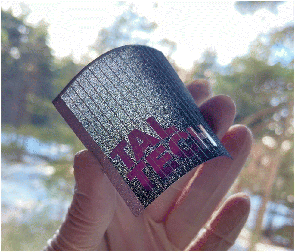 | ||
| Fig. 1 Photo of the MGL solar cell prototype. | ||
In this study, Cu2ZnSnS4 was synthesized in the form of MGPs using LiI, NaI, KI, RbI and CsI as a flux material. Properties of these alkali iodide salts are appropriate for the synthesis of CZTS MGPs: they have lower melting temperature (LiI – 469 °C,6 NaI – 651 °C, KI – 681 °C, RbI – 642 °C and CsI – 626 °C7) than the melting temperature of Cu2ZnSnS4 (990 °C);8 they have also high solubility in water at 25 °C (LiI – 1670 g L−1, NaI – 1842 g L−1, KI – 1428 g L−1, RbI – 1520 g L−1 and CsI – 848 g L−1),9 that allows to remove the flux by a simple dissolution in water after the synthesis-growth process. So far, KI have been successfully used as a flux material for growth of monograin powders of various solar absorber materials.10–14 However, there are no studies on the effect of other alkali metal iodides as flux materials on the properties of CZTS MGPs and the optoelectronic properties of MGL solar cells. Gaining a deeper understanding and better knowledge would create opportunities to expand the technological possibilities. Furthermore, several studies have shown the positive effect of alkali metals on the parameters of kesterite based thin film solar cells.15–20 The observed positive effects include an increase in the carrier concentration, improved charge transport properties, enhanced open-circuit voltage, and higher overall device efficiency. Alkali metals can facilitate the formation of favourable band alignment, reduce defect density, and passivate grain boundaries, thus leading to improved optoelectronic properties and device performance. It is worth noting that the specific mechanisms underlying the positive effects of alkali metals on kesterite solar cells are still under investigation, and the optimal concentration and incorporation methods may vary depending on the specific materials, fabrication technology and device architecture.
The research presented here focused on investigating the influence of different alkali iodide salts (LiI, NaI, KI, RbI and CsI) as flux materials on the properties of pure sulfide (CZTS) monograin powder crystals and the characteristics of monograin layer solar cells.
2. Experimental
2.1 Preparation of CZTS monograin powders
The monograin powders with initial composition of Cu1.84Zn1.09Sn0.99S4 were synthesized from high purity (5 N) CuS, SnS and ZnS binaries by isothermal molten salt synthesis-growth method in the presence of molten LiI (TM = 469 °C),6 NaI (TM = 651 °C), KI (TM = 681 °C), RbI (TM = 642 °C) and CsI (TM = 626 °C)7 salts as flux materials. The used precursor compounds CuS and SnS were self-synthesized from high purity Cu and Sn shots (5N, Alfa Aesar), and sulfur pieces in evacuated quartz ampoules, ZnS was commercially available. Due to the hygroscopic nature of LiI and NaI, it is necessary to prepare synthesis samples in a glove box within a dry environment to ensure optimal and similar conditions. The initial composition of CZTS was selected based on our research group previous experiments and as the best solar cell results have been achieved using this chemical composition.21–23 The volume ratio of solid precursors for CZTS to the flux salt was kept constant VCZTS/Vflux (cm3/cm3) = 1. The amount of the components for the kesterite synthesis and the amount of the flux material were taken nearly equal as it is important in monograin powder technology to provide enough volume of the liquid phase for filling the free volume between the solid particles.24,25 The precursors were weighed in desired amounts and ratios, grinded in an agate mortar to improve the homogeneity of mixture and loaded into quartz ampoules. The mixtures in ampoules were degassed under dynamic vacuum at 100 °C and sealed. The syntheses were performed in sealed vacuum quartz ampoules by heating at 740 °C for 136 hours. After the synthesis-growth, the ampoules were naturally cooled to RT, opened, and the flux material was removed by washing the powders with distilled water. After drying in hot-air oven at 50 °C, the powders were sieved into narrow granulometric fractions (between 36 and 125 μm) by sieving system Retsch AS 200.2.2 Preparation of CZTS monograin layer solar cells
Before implementing the monograins as absorber layer in MGL solar cells with the structure of Au/CZTS/CdS/i-ZnO/ZnO:Al/Ag/glass, the as-grown MGPs were individually subjected to chemical etching for 5 min with 1% v/v Br2–MeOH solution followed by 10% m/m aqueous solution of KCN etching for 5 min.26 Etched CZTS monograin powders were subsequently post-annealed in a dual-zone tube furnace in sealed ampoules at 840 °C under sulfur pressure of 2050 torr for 1 hour.21 Post-treatments are necessary to enhance the crystallinity of the powders, eliminate secondary phases, and improve the solar cell properties in general. The post-treated crystals were covered with CdS buffer layer by chemical bath deposition to form heterojunction. After buffer layer deposition, a soft annealing at 200 °C for 10 min was applied. In the MGL solar cells, every single CZTS crystal covered with the CdS buffer layer works as an individual solar cell. CZTS crystals stand separately without contacting each other and are bound together with a thin layer of epoxy. The scheme of MGL solar cell structure can be found elsewhere.27 The photoactive MGL (membrane) was formed by embedding the CdS covered CZTS crystals halfway to a thin epoxy layer (on a supporting plastic foil substrate). The thickness of the epoxy layer is determined by the range of grain size used for membrane preparation (for example 45–56 μm, 56–63 μm, 63–75 μm, 75–80 μm, 80–90 μm, 90–100 μm, etc.). After polymerization of epoxy, the membranes were covered by i-ZnO layer with thickness about 40–45 nm and a conductive ZnO:Al window layer with thickness about 800–900 nm using radio frequency magnetron sputtering system. The silver paste was used to make the front collector onto the ZnO window layer, and the front contact side of the structure was glued onto a glass plate. After removal of the supporting plastic foil from the structure, the surfaces of powder crystals at the back contact side were opened partly from the epoxy by etching with concentrated H2SO4 for determined times. After etching, the crystals’ surfaces of the back contact side were activated by a mechanical abrasive treatment. Subsequently, the gold back contacts with an area of 0.045 cm2 were deposited by thermal evaporation method.2.3 Characterization
The morphology of the synthesized (as-grown) CZTS powder crystals was investigated using a Zeiss Ultra 55 high-resolution scanning electron microscope (SEM). In-lens secondary electron detection at accelerating voltage of 4 kV was used. The chemical composition of the as-grown powder crystals’ bulk was determined by energy-dispersive X-ray microanalysis (EDX) on Bruker Esprit 1.82 EDX system equipped with EDX-XFlash 3001 detector at an accelerating voltage of 20 kV (the measurement error is about 0.5 at%). The micro-Raman spectra were recorded by using a Horiba LabRam HR800 spectrometer and a 532 nm laser line that was focused on the sample with a spot size of about 5 μm. Powder X-ray diffraction (XRD) patterns were recorded on a Rigaku Ultima IV diffractometer with Cu Kα radiation (λ = 1.5406 Å). PDXL 2 software was used for the derivation of crystal structure information from powder XRD data. For photoluminescence (PL) measurements, the powder samples were mounted in a closed-cycle He cryostat and cooled down to 8 K. A 441 nm He–Cd laser line was used for PL excitation and the spectra were detected by using an InGaAs detector. A focused laser beam with a spot size of about 3 mm was used. It means that the PL spectrum corresponds to at least 400 crystals. The measurement error in the values of the PL peak positions is 0.005 eV.The CZTS monograin layer solar cells were characterized by measuring the current versus voltage (J–V) characteristics by Keithley 2400 source meter under standard test conditions (AM 1.5, 100 mW cm−2) using a Newport Oriel Class A 91195A solar simulator. As the working area of the MGL solar cells is around 75% of the total area,28 the MGL solar cell efficiency values were re-calculated for the active area (ηactive). Spectral response measurements were performed in the spectral region of 350–1100 nm using a computer-controlled SPM-2 prism monochromator. The generated photocurrent was detected at 0 V bias voltage at RT by using a 250 W halogen lamp. Temperature-dependent J–V curve measurements were made using a Keithley 2401 source meter. The solar cells were mounted on the cold finger of a closed-cycle He cryostat (T = 20–320 K).
3. Results and discussion
3.1 Properties of CZTS monograin powders
Morphology studies by SEM confirmed that the shape of the formed crystals is influenced by the nature of the used flux materials (see Fig. 2). The CZTS crystals grown in LiI resulted in well-formed individual non-aggregated crystals. The crystal shapes were observed to be uniformly round, with rounded but porous edges (see Fig. 2(a)). In the crystal growth process, the round shape of crystals indicates high solubility of precursors and/or formed compound (CZTS) in used flux material. The CZTS crystals obtained through monograin synthesis-growth in NaI and KI exhibit a tetragonal shape, characterized by distinct sharp edges and smooth flat planes (Fig. 2(b) and (c)). This kind of shape is typical for tetragonal structured crystals, which form under conditions where the solubility of the target compound is relatively low. For example, the solubility of Cu2ZnSnSe4 in KI was determined to be 0.61 mol% at 740 °C.29Fig. 2(d) shows SEM micrographs of CZTS powder crystals grown in RbI. The powder consists of sintered and non-aggregated crystals. The individual crystals have flat and smooth facets with sharp edges. The agglomerated crystals have different, uneven shapes with rough edges and irregularities of porous surfaces. The coexistence of sintered and non-aggregated crystals suggests that parallel processes occur simultaneously. On the one hand, the monograin growth, which involves the formation of individual crystals through the molten phase. On the other hand, the sintering process occurs, where the formed crystals bond together. CZTS powder crystals grown in CsI molten salt resulted in uniform and non-aggregated crystals with smooth facets and round edges (see Fig. 2(e)).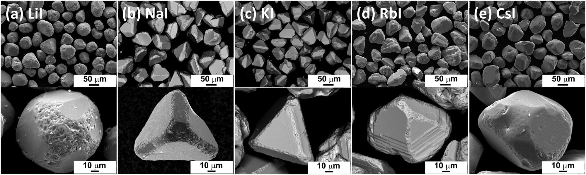 | ||
| Fig. 2 SEM images of CZTS MGP crystals grown in (a) LiI, (b) NaI, (c) KI, (d) RbI and (e) CsI molten salts. | ||
XRD patterns of CZTS MGPs grown in LiI, NaI, KI, RbI and CsI molten salts are displayed in Fig. 3. All the diffraction peaks including the major peaks (101), (112), (220) and (312) could be indexed according to a tetragonal kesterite type phase structure (ICDD: 01-084-8521) and correlates well with Mai et al.30 No secondary phases were detected. XRD pattern of CZTS MGPs grown in LiI (red line) revealed a shift of the diffraction peaks towards lower angles. The enlarged view of the shift of (112) lattice plane diffraction peak from 28.45° to 28.40° is presented in the inset graph in Fig. 3. Furthermore, the crystals grown in LiI exhibited larger lattice parameters values (a, b and c) compared with to the powders formed using NaI, KI, RbI and CsI as flux materials (see Fig. 4(a)). This kind of behavior indicates the incorporation of Li into the CZTS compound from the molten salt of LiI. Most probably, the Li+ ions (r = 0.76 Å) partly replaced the Cu+ ions (r = 0.74 Å) causing the expansion in the lattice.22,31 The obtained values are in good agreement with the results reported in the literature.32 Balboul et al. showed a correlation between the c/2a ratio, composition and efficiency in CuIn1−xGaxSe2 materials and concluded that the lowest electronic defect density occurs due to the smallest possible crystallographic distortion of the tetragonal lattice. In addition, the maximum efficiency was achieved at c/2a ≈ 1.0.33
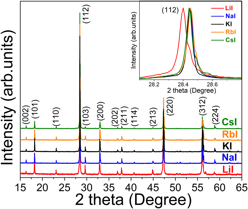 | ||
| Fig. 3 X-ray diffraction patterns of the CZTS MGPs grown in LiI, NaI, KI, RbI and CsI molten salts. The inset graph presents the enlarged view of the shift of the (112) diffraction peak positions. | ||
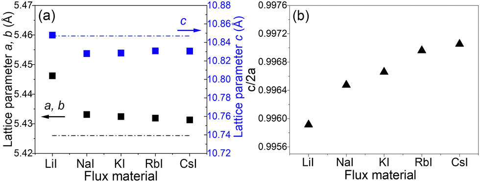 | ||
| Fig. 4 (a) Lattice parameters a, b, c and (b) c/2a of the CZTS MGPs grown in LiI, NaI, KI, RbI and CsI molten salts. The dashed lines represent the lattice constants of CZTS single crystal grown without alkali iodide salt as a reference point.30 | ||
Thus, it can be concluded that the highest efficiency is achieved when the composition results in an ideal tetragonal lattice with minimal disorder and defect density. Changing the c/2a ratio, which affects the tetragonality of the lattice, leads to lattice distortion. This distortion is likely to increase the concentration of crystallographic defects and potentially the concentration of electronic defects. Consequently, the efficiency of solar cells should decrease. In our experiments, powders grown in CsI showed the smallest tetragonal lattice distortion with a ratio of c/2a = 0.9971 (Fig. 4(b)). While powders grown in LiI show the largest tetragonal distortion with the ratio of c/2a = 0.9959.
The EDX results of the average concentration ratio values of Cu/(Zn + Sn) and Zn/Sn of the synthesised CZTS monograin powders are presented in Fig. 5(a). The average elemental ratios of CZTS powders were calculated from the EDX measurements of the cross-section of 8 different crystals. Fig. 5(a) gives an overview of how the respective outcome chemical composition of CZTS changes by using different flux materials i.e., LiI, NaI, KI, RbI and CsI. In input composition of CZTS the elemental ratios were Cu/(Zn + Sn) = 0.88 and Zn/Sn = 1.1. Elemental compositions determined by EDX analysis revealed that all the used flux materials resulted in a CZTS composition that was Cu-poor and Zn-rich. However, there were noticeable differences in the concentrations of Cu and Zn within the bulk of the crystals, which varied depending on the specific flux material utilized. The concentration of Cu in crystals’ bulk increased and the concentration of Zn decreased linearly in the order of used flux materials from LiI, NaI, KI, RbI to CsI. Although, in the case of all powders the ratio of Zn/Sn (varied from 1.04 to 1.07) was lower than the input ratio of 1.1 and the ratio of Cu/(Zn + Sn) (varied from 0.91 to 0.94) was higher than the input ratio of 0.88 except for the powder grown in LiI. The decrease in Zn content in the final powder composition is most likely a result of some unreacted ZnS precursor.13,34 As a result, the composition of the material shifts towards a higher copper content. The powder synthesised in LiI showed a ratio of Cu/(Zn + Sn) = 0.87, which is much lower compared to other materials and is probably related to the replacement of Cu ions by Li in crystal lattice. Among the used flux materials, CsI resulted in the production of monograin powder with a chemical composition that was closest to stoichiometry for CZTS (Cu/(Zn + Sn) = 0.94 and Zn/Sn = 1.04).
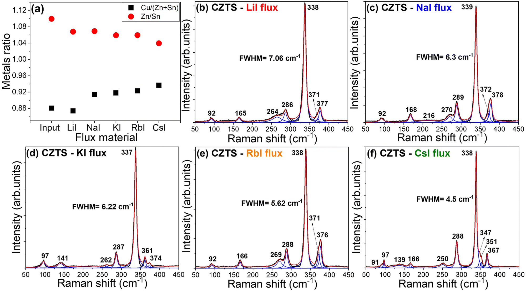 | ||
| Fig. 5 (a) Cu/(Zn + Sn) and Zn/Sn compositional ratios of the CZTS MGP crystals depending on the used flux material as determined by EDX. (b)–(f) Raman spectra of CZTS MGP crystals grown in LiI, NaI, KI, RbI and CsI molten salts. | ||
To support the findings obtained through XRD and EDX analyses regarding the CZTS MGPs grown in different flux materials, room temperature Raman analysis was carried out. Raman spectra are presented in Fig. 5(b)–(f). The Lorentzian function was used for fitting to resolve all the Raman peaks. Raman analysis of all five analysed samples revealed that all detected peaks could be attributed to the CZTS phase with the sharp characteristic peak in the range of 337–339 cm−1.35,36 A trace of ZnS, peak at 351 cm−1![[thin space (1/6-em)]](https://www.rsc.org/images/entities/char_2009.gif) 37 was detected in the CZTS MGPs grown in CsI. The full width at half maximum (FWHM) of 7.06 cm−1 to 4.5 cm−1 in the order of used flux materials from LiI, NaI, KI, RbI to CsI (Fig. 5(b)–(f)). The width of this peak gives a hint about crystallinity and structural distribution. This means that a material with high crystallinity is characterized by sharp and narrow peaks in the Raman spectra. In our case, the CZTS MGPs grown in LiI showed the widest mode of the main Raman peak (FWHM = 7.06 cm−1). This finding supports the XRD results and proves the incorporation of Li from LiI into the lattice structure. In the case of CsI, Raman peaks are sharper and narrower (FWHM = 4.5 cm−1) compared to the other produced powders, showing a higher level of crystallinity.
37 was detected in the CZTS MGPs grown in CsI. The full width at half maximum (FWHM) of 7.06 cm−1 to 4.5 cm−1 in the order of used flux materials from LiI, NaI, KI, RbI to CsI (Fig. 5(b)–(f)). The width of this peak gives a hint about crystallinity and structural distribution. This means that a material with high crystallinity is characterized by sharp and narrow peaks in the Raman spectra. In our case, the CZTS MGPs grown in LiI showed the widest mode of the main Raman peak (FWHM = 7.06 cm−1). This finding supports the XRD results and proves the incorporation of Li from LiI into the lattice structure. In the case of CsI, Raman peaks are sharper and narrower (FWHM = 4.5 cm−1) compared to the other produced powders, showing a higher level of crystallinity.
3.2 Photoluminescence studies
Temperature and excitation power dependent photoluminescence (PL) measurements were conducted to investigate the recombination mechanisms in CZTS MGP crystals grown in different alkaline salts. At a temperature of 8 K, all samples exhibited a broad asymmetric PL band, characterized by an exponential tail on the low-energy side. Normalized PL spectra are presented in Fig. 6. All samples displayed a similar shape and a peak position, with the maximum energy (Emax) approximately equal to 1.262 eV. The exponential tail is determined by the density of states function and is typical for kesterites with quite deep electrostatic potential and/or band gap fluctuations.38,39 The average depth γ of these fluctuations is found to be about 41 meV and similar values have been measured in our previous CZTS samples.40 The observed blue-shift of PL band peak position with increasing laser power indicates the presence of band edge fluctuations. All samples show quite similar blue-shift of 10 meV per decade of laser power and this is quite common for CZTS value, where band-edge fluctuations are present.41,42 The integrated PL band intensity Φ for all samples at T = 8 K exhibits a power-law dependence on the excitation power, which can be described by the equation Φ ∼ Pk, where P represents the excitation power and k is the exponent. The k-value, which is an indication of the type of recombination, resulted in 0.86 for all samples. This is evidence that the recombination is defect related.43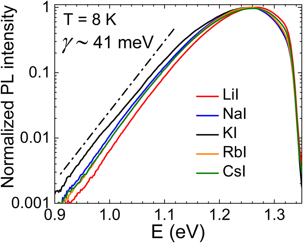 | ||
| Fig. 6 Normalized low-temperature photoluminescence spectra and the average depth of potential fluctuations γ in Cu2ZnSnS4 MGPs grown in LiI, NaI, KI, RbI and CsI molten salts. | ||
The temperature dependent PL measurements revealed a noticeable red-shift in the peak position for all samples. Importantly, the rate of this red-shift was found to be faster than the temperature dependence of band gap energy Eg, see Fig. 7. This rapid red-shift is usually caused by the redistribution of holes between shallow and deep potential wells or deep acceptor levels.44
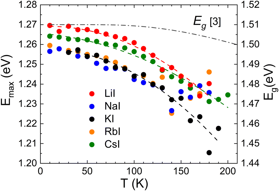 | ||
| Fig. 7 The temperature dependence of the PL peak position (Emax) for all samples together with the dependence of band gap energy Eg.45 | ||
The theoretical formula for discrete energy levels was used to fit the temperature quenching of the PL band across all samples:46
| Φ(T) = Φ0/[1 + A1T3/2 + A2T3/2exp(−EA/kT)] | (1) |
 | ||
| Fig. 8 Thermal activation energies measured from Cu2ZnSnS4 MGPs grown in LiI, NaI, KI, RbI and CsI molten salts. | ||
3.3 Device characterization
Additional research was conducted to investigate the characteristics of solar cells fabricated using Cu2ZnSnS4 monograin powders grown in molten LiI, NaI, KI, RbI and CsI.Fig. 9 shows the impact of the five different flux materials used on output parameters of the MGL solar cells. The box plots present the values of short circuit current density (Jsc), open circuit voltage (Voc), fill factor (FF), and the efficiency, providing a comparative analysis of their respective influences. Data are extrapolated from the analysis of 10 solar cells. Among the five flux materials used, the highest power conversion efficiencies achieved are as follows: LiI (5.3%), NaI (9.4%), KI (10.6%) RbI (9.9%) and CsI (10.9%). The values of fill factor and short circuit current density also exhibited variations across the different materials used. Solar cells based on CsI grown powder showed the highest FF of 65% and Jsc of 23.4 mA cm−2. Conversely, solar cells based on LiI grown powder exhibited the lowest FF of 59.6% and Jsc of 15 mA cm−2. Among the flux materials NaI, KI and RbI, the mean values of Jsc range from 20.8 to 22.5 mA cm−2. Specifically, KI shows the highest Jsc values, while NaI shows the lowest values. The mean values of FF for NaI, KI and RbI fluctuated in the range of 59–63%, being highest in the case of KI. Furthermore, the Voc for solar cells using CZTS grown in LiI was exceptionally low at 602 mV. On the other hand, solar cells based on powders grown in CsI demonstrated the highest Voc value of 734 mV. Except for LiI, the average values of Voc for all other flux materials fall within a similar range, with only slight variations. The Voc values of the devices based on NaI, KI and RbI remained at the level of 712–725 mV. Thus, based on the solar cell parameters presented in Fig. 9, it can be concluded that both KI and CsI flux materials are viable choices for fabricating MGPs as absorber materials. The resulting solar cell performance using these flux materials exhibits comparable characteristics, although the highest efficiency was achieved with CZTS grown in CsI.
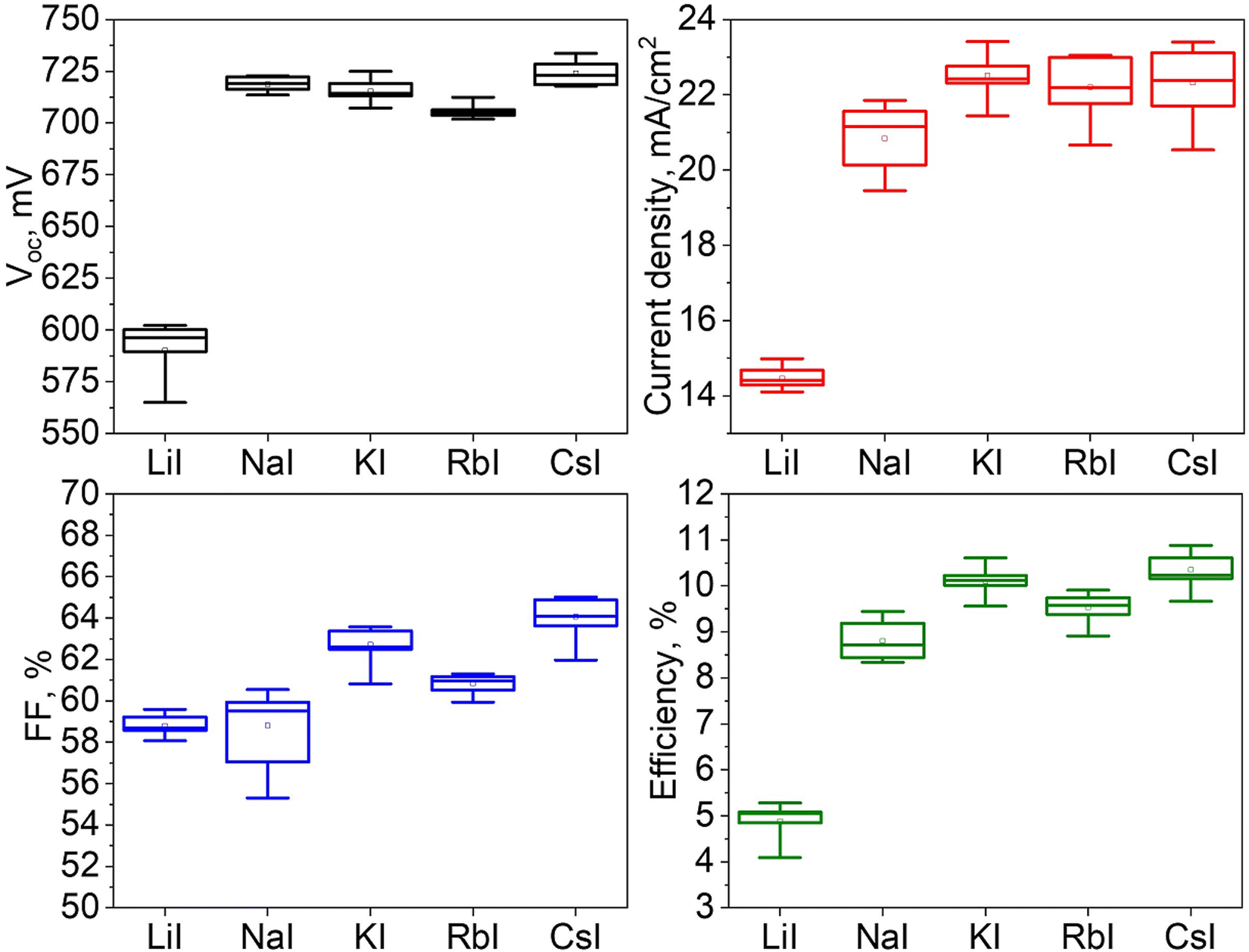 | ||
| Fig. 9 Box plots of the open circuit voltage, short-circuit current density, fill factor and efficiency of MGL solar cells fabricated from Cu2ZnSnS4 MGPs grown in LiI, NaI, KI, RbI and CsI molten salts. | ||
Due to the challenges associated with evaluating the band gap energy of monograin powders using optical absorption or reflectance spectra, an analysis of external quantum efficiency (EQE) was employed to estimate the effective band gap energy ( ) of the absorber materials. This method provides a reliable alternative for determining the band gap energy of the materials under investigation. Fig. 10 presents the normalized external quantum efficiency vs. wavelength plots for solar cells. From the linear segment of the low-energy side of the (E*EQE)2vs. E plots, the
  values are calculated (inset graph in Fig. 10). Herein, it must be pointed out, that the (E*EQE)2 method gives about 20 meV smaller band gap energy than could be found from absorption measurements.49
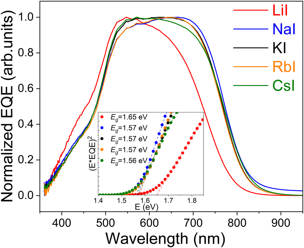 | ||
| Fig. 10 Normalized external quantum efficiency spectra of Cu2ZnSnS4 MGL solar cells, inset graph shows band gap extraction by plotting (E*EQE)2vs. E. | ||
Contradictory to the effective band gap energy values determined from the analysis of EQE (presented in Table 1), which indicates that the powder grown in LiI has the highest  value (1.65 eV), the corresponding Voc values are the lowest at around 600 mV. However, for all other powders, the determined
  values were lower approximately around 1.57 eV. The corresponding solar cell devices exhibited Voc values that were over 100 mV higher. The observed increase in band gap energy value correlates the findings from XRD and Raman results, providing evidence for the incorporation of Li from LiI into the lattice structure. This leads to the formation of the new solid solution, (Cu1−xLix)2ZnSnS4, which has different properties as an absorber material. This incorporation of Li and the resulting solid solution formation have a negative impact on the performance of the device, impairing its efficiency.
| Used salt | Φ B (eV) | Φ A (eV) |
|
R ser (300 K) (Ω cm2) | E 00 (meV) | N A (cm−3) | n@300 K |
|---|---|---|---|---|---|---|---|
| LiI | 1.60 | 1.30 | 1.65 | 0.40 | 116 | 1.47 × 10¹⁷ | 3.9 |
| NaI | 1.92 | 1.29 | 1.57 | 1.50 | 150 | 2.38 × 10¹⁶ | 2.8 |
| KI | 1.26 | 1.31 | 1.57 | 0.57 | 49 | 9.90 × 10¹⁶ | 2.8 |
| RbI | 1.67 | 1.37 | 1.57 | 1.09 | 93 | 7.99 × 10¹⁶ | 2.9 |
| CsI | 1.27 | 1.25 | 1.56 | 0.89 | 58 | 1.28 × 10¹⁷ | 2.3 |

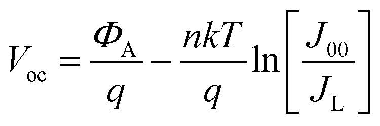
Temperature-dependent J–V curve measurements were employed to gain further insights into the recombination mechanisms and to evaluate the junction quality. The behaviour of the Voc of the cells as a function of temperature is shown in Fig. 11 and can be described by the following equation:
 | (2) |
 and ΦA values from the Vocversus temperature measurement, and the interface recombination is the predominant recombination mechanism. The difference between
  and ΦA values was highest (0.35 eV) in the solar cells prepared from powders grown in LiI and lowest (0.20 eV) by using powders grown in RbI as absorber material.
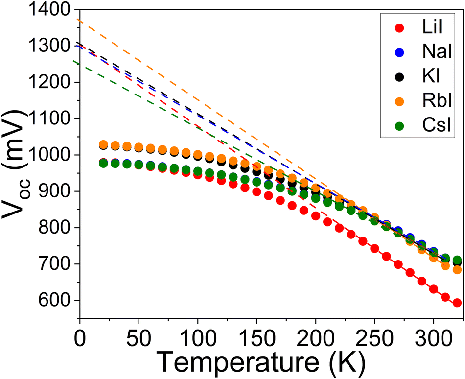 | ||
| Fig. 11 V oc–T measurements of the Cu2ZnSnS4 MGL solar cells. Dashed lines present the extrapolation of the linear part of the Voc–T at T = 0 K for the determination of ΦA. | ||
While the J–V curve parameters at ambient temperature do not change significantly, the temperature dependency of identical cells reveals extremely distinct behavior. We used a single diode equation to fit all the light J–V curves:
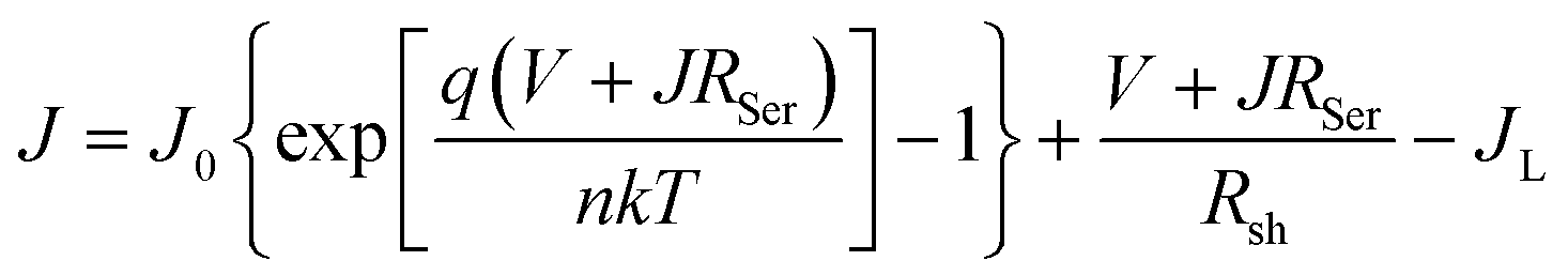 | (3) |
 | (4) |
The most important parameters obtained from the fittings are given in Table 1.
The diode ideality factor n values as a function of temperature typically provide comprehensive information about possible recombination mechanisms in solar cells.52,53 It was demonstrated that the temperature dependence of the ideality factor in the case of tunneling assisted interface recombination is given by:52
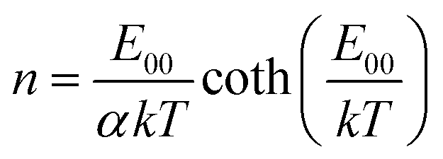 | (5) |
| E00 = (qℏ/2)[NA/(m × ε)]0.5 | (6) |
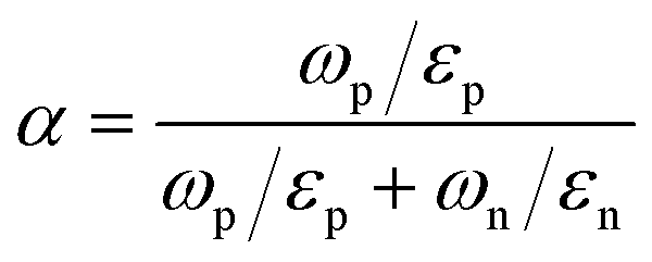 | (7) |
From the single diode model for the J0, the following expression can be derived:
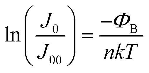 | (8) |
 | (9) |
ln(J0) versus 1/kT should yield a straight line with a slope corresponding to the activation energy of the saturation current ΦB, see Fig. 12.
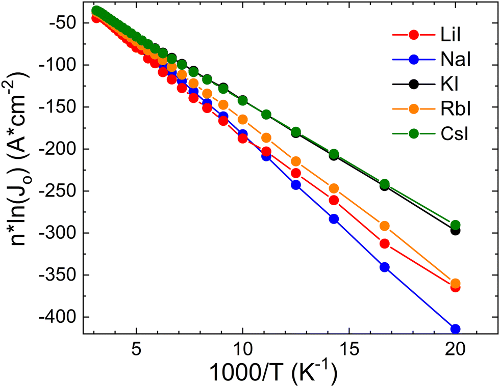 | ||
| Fig. 12
nln(J0) vs. 1000/T plot. Obtained values of ΦB are given in Table 1. | ||
It is known that values ΦB< Eg would indicate interface recombination as the dominant mechanism due to Fermi-level pinning or band gap narrowing at the interface. However, we see extremely high values of ΦB in some samples, see for example NaI and RbI (Table 1). Also, the LiI sample shows not a typical behavior, and it is related to abnormal temperature dependence of ideality factor n. Low temperature J–V measurements thus reveal different recombination channels which are missing at room temperature.
We also measured C–V curves at room temperature to get information about carrier concentration. As can be seen from Table 1, the carrier concentration (NA) of all samples is in the range of 1017 cm−3 and confirms the previous statement, that room temperature properties of all samples are quite similar.
Based on the results of current research, we can conclude that for the technological conditions used in this experimental work, KI and CsI have been found to be the most useful flux materials to enhance PV performance of CZTS MGL solar cells, and LiI as the least suitable.
4. Conclusions
It was found that the synthesis-growth of CZTS MGP crystals is possible in all used molten alkali fluxes. SEM and EDX studies showed that the morphology and composition of the formed crystals are influenced by the nature of the flux materials. Structural studies by XRD showed good crystallinities for all MGPs but revealed lattice expansion of powder grown in LiI. The same powder also showed the widest main Raman peak with FWHM of 7.06 cm−1. According to the Raman and XRD analysis, the growth of CZTS MGP in CsI resulted in a higher level of crystallinity and smallest lattice distortion compared to other produced powders. Low-temperature (T = 8 K) photoluminescence spectra of all the CZTS MGPs were dominated by single broad asymmetric photoluminescence bands with maxima at about 1.26 eV and thermal quenching activation energies of about 130 meV. The tunneling enhanced interface recombination was discovered to be the dominant process in all materials. At low temperatures, recombination channels that were absent at room temperature were revealed for powder crystals grown in LiI, NaI, and RbI. The effective band gap energy values were determined to be ∼1.57 eV for CZTS powders grown in NaI, KI, RbI and CsI. The of absorber material grown in LiI increased to 1.65 eV, but corresponding solar cell showed 100 mV lower Voc value compared to solar cells based on other MGPs. All results confirmed Li+ incorporation from the molten flux (LiI) into the Cu2ZnSnS4 crystal's structure, resulting in the formation of a new (Cu1−xLix)2ZnSnS4 solid solution. The highest efficiency of 10.9% was achieved with MGL solar cell based on CZTS grown in CsI showing output parameters: Voc = 718 mV, Jsc = 23.4 mA cm−2 and FF = 65%. Although CsI resulted in the highest efficiency, it is important to consider other factors such as cost, stability, and scalability when selecting a suitable flux material for large-scale production. Further research and analysis may be required to fully understand the advantages and limitations of each flux material, including their impact on long-term stability, manufacturing cost, and overall device performance.
Author contributions
Kristi Timmo: writing – original draft, project administration, investigation, formal analysis, data curation. Maris Pilvet: methodology, investigation. Katri Muska: methodology, investigation. Mare Altosaar: methodology, investigation. Valdek Mikli: investigation, formal analysis. Reelika Kaupmees: formal analysis, data curation. Raavo Josepson: methodology, formal analysis. Jüri Krustok: writing – review & editing, investigation, formal analysis, data curation. Maarja Grossberg-Kuusk: funding acquisition. Marit Kauk-Kuusik: writing – review & editing, investigation, funding acquisition.Conflicts of interest
There are no conflicts to declare.Acknowledgements
This work was supported by European Union through the European Regional Development Fund, Project TK141, by the European Union's H2020 research and innovation program under grant agreement no. 952982 (Custom-Art project), and by the Estonian Research Council grant PRG1023.References
- S. Hadke, M. Huang, C. Chen, Y. F. Tay, S. Chen, J. Tang and L. Wong, Chem. Rev., 2022, 122, 10170–10265 CrossRef CAS PubMed.
- K. Pal, P. Singh, A. Bhaduri and K. B. Thapa, Sol. Energy Mater. Sol. Cells, 2019, 196, 138–156 CrossRef CAS.
- J. Zhou, X. Xu, H. Wu, J. Wang, L. Lou, K. Yin, Y. Gong, J. Shi, Y. Luo, D. Li, H. Xin and Q. Meng, Nat. Energy, 2023, 8, 526–535 CrossRef CAS.
- M. A. Green, E. D. Dunlop, G. Siefer, M. Yoshita, N. Kopidakis, K. Bothe and X. Hao, Prog. Photovol. Res. Appl., 2023, 31, 3–16 CrossRef.
- H. S. Nugroho, G. Refantero, N. L. W. Septiani, M. Iqbal, S. Marno, H. Abdullah, P. E. C. Nugraha and B. Yuliarto, J. Ind. Eng. Chem., 2022, 105, 83–110 CrossRef CAS.
- R. Sridhar, C. E. Johnson and E. J. Cairns, J. Chem. Eng. Data, 1970, 15, 244–245 CrossRef CAS.
- S. L. Baldochi and I. M. Ranieri, in Encyclopedia of Materials: Science and Technology, ed. K. H. J. Buschow, R. W. Cahn, M. C. Flemings, B. Ilschner, E. J. Kramer, S. Mahajan and P. Veyssière, Elsevier, Oxford, 2001, pp. 74–78 Search PubMed.
- H. Matsushita, T. Ichikawa and A. Katsui, J. Mater. Sci., 2005, 40, 2003–2005 CrossRef CAS.
- Database of HSC Chemistry Ver.6.0., Outoukumpu Research Oy, Pori, Finland Search PubMed.
- M. Kauk-Kuusik, M. Altosaar, K. Muska, M. Pilvet, J. Raudoja, K. Timmo, T. Varema, M. Grossberg, E. Mellikov and O. Volobujeva, Thin Solid Films, 2013, 535, 18–21 CrossRef CAS.
- M. Pilvet, M. Kauk-Kuusik, M. Altosaar, M. Grossberg, M. Danilson, K. Timmo, A. Mere and V. Mikli, Thin Solid Films, 2015, 582, 180–183 CrossRef CAS.
- K. Timmo, M. Kauk-Kuusik, M. Pilvet, M. Altosaar, M. Grossberg, M. Danilson, R. Kaupmees, V. Mikli, J. Raudoja and T. Varema, Sol. Energy, 2018, 176, 648–655 CrossRef CAS.
- K. Timmo, M. Altosaar, M. Pilvet, V. Mikli, M. Grossberg, M. Danilson, T. Raadik, R. Josepson, J. Krustok and M. Kauk-Kuusik, J. Mater. Chem. A, 2019, 7, 24281–24291 RSC.
- X. Li, M. Pilvet, K. Timmo, M. Grossberg, V. Mikli and M. Kauk-Kuusik, Sol. Energy, 2020, 209, 646–652 CrossRef CAS.
- Y. E. Romanyuk, S. G. Haass, S. Giraldo, M. Placidi, D. Tiwari, D. J. Fermin, X. Hao, H. Xin, T. Schnabel, M. Kauk-Kuusik, P. Pistor, S. Lie and L. H. Wong, J. Phys. Energy, 2019, 1, 044004 CrossRef CAS.
- A. Mule, B. Vermang, M. Sylvester, G. Brammertz, S. Ranjbar, T. Schnabel, N. Gampa, M. Meuris and J. Poortmans, Thin Solid Films, 2017, 633, 156–161 CrossRef CAS.
- Y. Wu, M. Zhao, D. Zhuang, N. Zhang, X. Yu, Y. Wei, X. Lyu, G. Ren, C. Wang, L. Hu, Y. Li, J. Wei and Q. Gong, Sol. Energy, 2019, 187, 269–273 CrossRef CAS.
- S. G. Haass, C. Andres, R. Figi, C. Schreiner, M. Bürki, A. N. Tiwari and Y. E. Romanyuk, AIP Adv., 2018, 8, 15133 CrossRef.
- B. Liu, J. Guo, R. Hao, L. Wang, K. Gu, S. Sun and A. Aierken, Sol. Energy, 2020, 201, 219–226 CrossRef CAS.
- J. Zhou, X. Xu, B. Duan, H. Wu, J. Shi, Y. Luo, D. Li and Q. Meng, Nano Energy, 2021, 89, 106405 CrossRef CAS.
- R. Chen, J. Fan, H. Li, C. Liu and Y. Mai, R. Soc. Open Sci., 2018, 5, 171163 CrossRef PubMed.
- K. Muska, K. Timmo, M. Pilvet, R. Kaupmees, T. Raadik, V. Mikli, M. Grossberg-Kuusk, J. Krustok, R. Josepson, S. Lange and M. Kauk-Kuusik, Sol. Energy Mater. Sol. Cells, 2023, 252, 112182 CrossRef CAS.
- M. Kauk-Kuusik, K. Timmo, K. Muska, M. Pilvet, J. Krustok, M. Danilson, V. Mikli, R. Josepson and M. Grossberg-Kuusk, J. Phys. Energy, 2022, 4, 24007 CrossRef.
- E. Mellikov, J. Hiie and M. Altosaar, Int. J. Mater. Prod. Technol., 2007, 28, 291–311 CrossRef CAS.
- J. Hiie, M. Altosaar, E. Mellikov, P. Kukk, J. Sapogova and D. Meissner, Phys. Scr., 1997, 1997, 155 CrossRef.
- K. Timmo, M. Altosaar, J. Raudoja, M. Grossberg, M. Danilson, O. Volobujeva and E. Mellikov, in 2010 35th IEEE Photovoltaic Specialists Conference, 2010, pp. 1982–1985.
- M. Kauk-Kuusik, K. Timmo, K. Muska, M. Pilvet, J. Krustok, R. Josepson, G. Brammertz, B. Vermang, M. Danilson and M. Grossberg, ACS Appl. Energy Mater., 2021, 4, 12374–12382 CrossRef CAS.
- C. Neubauer, E. Babatas and D. Meissner, Appl. Surf. Sci., 2017, 423, 465–468 CrossRef CAS.
- I. Klavina, T. Kaljuvee, K. Timmo, J. Raudoja, R. Traksmaa, M. Altosaar and D. Meissner, Thin Solid Films, 2011, 519, 7399–7402 CrossRef CAS.
- D.-L. Mai, H.-J. Park and I.-H. Choi, J. Cryst. Growth, 2014, 402, 104–108 CrossRef CAS.
- Y. E. Romanyuk, S. G. Haass, S. Giraldo, M. Placidi, D. Tiwari, D. J. Fermin, X. Hao, H. Xin, T. Schnabel, M. Kauk-Kuusik, P. Pistor, S. Lie and L. H. Wong, J. Phys. Energy, 2019, 1, 44004 CrossRef CAS.
- A. Lafond, C. Guillot-Deudon, J. Vidal, M. Paris, C. La and S. Jobic, Inorg. Chem., 2017, 56, 2712–2721 CrossRef CAS PubMed.
- M. R. Balboul, H. W. Schock, S. A. Fayak, A. A. El-Aal, J. H. Werner and A. A. Ramadan, Appl. Phys. A: Mater. Sci. Process., 2008, 92, 557–563 CrossRef CAS.
- W. E. Pottker, R. Ono, M. A. Cobos, A. Hernando, J. F. D. F. Araujo, A. C. O. Bruno, S. A. Lourenço, E. Longo and F. A. La Porta, Ceram. Int., 2018, 44, 17290–17297 CrossRef CAS.
- P. A. Fernandes, P. M. P. Salomé and A. F. da Cunha, Thin Solid Films, 2009, 517, 2519–2523 CrossRef CAS.
- M. Dimitrievska, A. Fairbrother, X. Fontané, T. Jawhari, V. Izquierdo-Roca, E. Saucedo and A. Pérez-Rodríguez, Appl. Phys. Lett., 2014, 104, 021901 CrossRef.
- Y. C. Cheng, C. Q. Jin, F. Gao, X. L. Wu, W. Zhong, S. H. Li and P. K. Chu, J. Appl. Phys., 2009, 106, 123505 CrossRef.
- G. Rey, G. Larramona, S. Bourdais, C. Choné, B. Delatouche, A. Jacob, G. Dennler and S. Siebentritt, Sol. Energy Mater. Sol. Cells, 2018, 179, 142–151 CrossRef CAS.
- M. Grossberg, J. Krustok, C. J. Hages, D. M. Bishop, O. Gunawan, R. Scheer, S. M. Lyam, H. Hempel, S. Levcenco and T. Unold, J. Phys. Energy, 2019, 1, 44002 CrossRef CAS.
- M. Grossberg, J. Krustok, J. Raudoja, K. Timmo, M. Altosaar and T. Raadik, Thin Solid Films, 2011, 519, 7403–7406 CrossRef CAS.
- A. Crovetto, S. Kim, M. Fischer, N. Stenger, A. Walsh, I. Chorkendorff and P. C. K. Vesborg, Energy Environ. Sci., 2020, 13, 3489–3503 RSC.
- S. Oueslati, M. Kauk-Kuusik, C. Neubauer, V. Mikli, D. Meissner, G. Brammertz, B. Vermang, J. Krustok and M. Grossberg, Sol. Energy, 2020, 198, 586–595 CrossRef CAS.
- T. Schmidt, K. Lischka and W. Zulehner, Phys. Rev. B: Condens. Matter Mater. Phys., 1992, 45, 8989–8994 CrossRef PubMed.
- J. Krustok, H. Collan, M. Yakushev and K. Hjelt, Phys. Scr., 1999, 1999, 179 CrossRef.
- W. Li, K. Jiang, J. Zhang, X. Chen, Z. Hu, S. Chen, L. Sun and J. Chu, Phys. Chem. Chem. Phys., 2012, 14, 9936–9941 RSC.
- J. Krustok, H. Collan and K. Hjelt, J. Appl. Phys., 1997, 81, 1442–1445 CrossRef CAS.
- S. Chen, L.-W. Wang, A. Walsh, X. G. Gong and S.-H. Wei, Appl. Phys. Lett., 2012, 101, 223901 CrossRef.
- M. Grossberg, T. Raadik, J. Raudoja and J. Krustok, Curr. Appl. Phys., 2014, 14, 447–450 CrossRef.
- R. Carron, C. Andres, E. Avancini, T. Feurer, S. Nishiwaki, S. Pisoni, F. Fu, M. Lingg, Y. E. Romanyuk, S. Buecheler and A. N. Tiwari, Thin Solid Films, 2019, 669, 482–486 CrossRef CAS.
- J. Krustok, R. Josepson, M. Danilson and D. Meissner, Sol. Energy, 2010, 84, 379–383 CrossRef CAS.
- S. Suckow, T. M. Pletzer and H. Kurz, Prog. Photovol. Res. Appl., 2014, 22, 494–501 CrossRef.
- V. Nadenau, U. Rau, A. Jasenek and H. W. Schock, J. Appl. Phys., 2000, 87, 584–593 CrossRef CAS.
- U. Rau, A. Jasenek, H. W. Schock, F. Engelhardt and T. Meyer, Thin Solid Films, 2000, 361–362, 298–302 CrossRef CAS.
| This journal is © The Royal Society of Chemistry 2023 |