DOI:
10.1039/D3MA00424D
(Paper)
Mater. Adv., 2023,
4, 4520-4527
Photo-enhanced metal-assisted chemical etching of α-gallium oxide grown by halide vapor-phase epitaxy on a sapphire substrate and its applications†
Received
17th July 2023
, Accepted 1st September 2023
First published on 5th September 2023
Abstract
The development of an etching process with controllable etching rate and high selectivity is key to fabricating high-performance electronic and optoelectronic devices. In this paper, we report the photo-enhanced metal-assisted chemical (PE-MAC) etching of an ultrawide-bandgap (UWBG) alpha-phase gallium oxide (α-Ga2O3) semiconductor grown using a halide vapor-phase epitaxy technique. Using the PE-MAC etching process, the reproducible etch of an α-Ga2O3 epilayer was demonstrated at a rate of 8.24 nm min−1 at room temperature; the extent of the reaction increased linearly with increasing time. The Arrhenius plot of the etching rate indicated that this process is an activation-controlled reaction with a high activation energy of 0.90 eV (86.7 kJ mol−1). The Pt metal electrode, which can be removed using an acid solution, created a depletion region, making the exposed α-Ga2O3 epilayer etched with a smooth and tilted sidewall. The effects of the roughness at different etch temperatures were also investigated. An α-Ga2O3-based metal–semiconductor–metal (MSM) photodetector was fabricated by using the proposed PE-MAC etching process, and the fabricated MSM photodetector exhibited improved time-dependent photoresponse characteristics with reduced defect-related time constants, confirming that our PE-MAC etching is a damage-free fabrication process with high anisotropy and selectivity. Our study demonstrates that the PE-MAC etching is an effective wet process for manufacturing electronic and optical devices based on UWBG α-Ga2O3 semiconductors at room temperature without vacuum plasma equipment.
Introduction
Alpha-phase gallium oxide (α-Ga2O3) is an ultrawide-bandgap (UWBG) semiconductor material with great potential for next-generation high-power electronic and deep ultra-violet (UV) photodetector devices because it has the largest energy bandgap (∼5.3 eV) and breakdown field (9.5 MV cm−1) of the five known phases of gallium oxide (Ga2O3) (α, β, γ, δ and ε).1–3 Owing to its ultrawide bandgap energy, α-Ga2O3 is not responsive to visible and UV-A/B wavelengths but selectively reacts to light in the UV-C region, making it an ideal candidate for a solar-blind photodetector (PD).4,5 The high breakdown fields of α-Ga2O3 compared with Si and other wide-bandgap semiconductors, including GaN and SiC, allow it to resist strong electric fields applied under high-power conditions, enabling low-loss and high-voltage operation.6 The bandgap engineering of α-Ga2O3 has been investigated by alloying it with various metals (Ti, Al, Fe, Cr and In) and fabricating versatile α-Ga2O3-based (opto)electronic devices.7 Baliga's figure of merit (BFOM) is a metric to evaluate the conduction loss of a power semiconductor material and is calculated using 4VB2/εμEg3, where VB stands for the breakdown voltage, ε is the dielectric constant, μ is the carrier mobility and Eg is the energy bandgap.8 The BFOMs of α-Ga2O3 is 2.19 times higher than that of GaN. Furthermore, the BFOMs of α-Ga2O3 is 1.64 times higher than that of β-Ga2O3, indicating superior performance of α-Ga2O3 and demonstrating its potential for use in next-generation power electronics.9–11 The devices and the processing of β-Ga2O3 have been extensively studied; however, few studies have been thus far reported on the devices and processing of α-Ga2O3.
As semiconductor devices become increasingly integrated, the importance of controllable etching for producing finely detailed patterns is increasing. The development of a damage-free etching technology that can produce a uniform etching pattern with high anisotropy is required, allowing the manufacture of electronic and optoelectronic devices that utilize the full potential of α-Ga2O3.12 The use of high-density plasma for the anisotropic etching of α-Ga2O3 has been investigated by using chlorine-based inductively coupled plasma (ICP) at an etch rate of 33 nm min−1 with plasma power of 200 W, where a linear relationship was observed between the plasma power and etching rate.13 Dry etching techniques using high-density plasma offer various advantages, such as anisotropy and control of the etching rate by manipulating the plasma power. However, plasma-induced defects can degrade the device performance by increasing the leakage currents or decreasing the free-carrier concentrations.14,15 In contrast, wet (chemical) etching offers a vacuum-free and low-energy-consumption process compared with plasma etching and can prevent the device performance degradation due to plasma-induced damage. In addition, wet etching can be used as a cleaning process to restore the pristine surface.12,16 However, previously reported wet etching processes typically exhibit an isotropic etching mechanism and are not suitable for device fabrication owing to considerably low etching rates at room temperature. Choi et al. etched α-Ga2O3 using a SiO2 etch mask in HCl solution, where the etching was achieved by reacting Ga2O3 with HCl to produce GaCl3. Below the process temperature of 40 °C, the etching rate was less than 5 nm min−1, suggesting very low reactivity.17 Zhang et al. etched β-Ga2O3 using phosphoric acid but did not achieve a suitable etching rate at temperatures below 140 °C (compared with a rate of 2 nm min−1 at 160 °C).18 Chemical etching using an acidic solution at elevated temperatures is generally not preferred because it can generate toxic gases.
Unlike conventional wet etching, metal-assisted chemical (MAC) etching uses a metal catalyst to achieve anisotropic etching and high selectivity.19 A cathodic reaction in the metal catalyst and anodic reaction in the target material are the two key mechanisms in MAC etching. The metal removes electrons from the material to be etched and leaves holes at the interface with the material. The metal is then re-oxidized by oxidants. Subsequently, the material reacts with the holes to form ions, which makes it more reactive with the etchant. The MAC etching of Si has been reported with several metal catalysts (Au, Pd, and Pt) and hydrofluoric acid (HF) with hydrogen peroxide (H2O2).20 Chern et al. produced Si nanowires with a high aspect ratio through MAC etching using Pt metal and HF.21 Because the accumulation of holes is an essential mechanism of MAC etching, the hole concentration is a crucial parameter to initiate and maintain the etching process. A photo-enhanced (PE) MAC etching method using UV wavelengths was developed to accumulate sufficient concentration of holes in WBG semiconductors. MAC etching involves a catalytic reaction of the metal, and etching proceeds at the interface between the metal and the target material. In contrast, the PE-MAC etching reaction occurs in the area not in contact with the metal (irradiated by UV light).22 In addition, in the PE-MAC etching reaction, it is convenient to adjust the etching time by controlling the UV light source. The MAC and PE-MAC etching for InP substrates were demonstrated in the dark and under UV light.23 The etchant consisted of H2SO4 and H2O2 oxidants, and the UV light for PE-MAC etching was generated by a mercury lamp (290–390 nm). In the dark, MAC etching occurred, and the InP in the region in contact with the metal was selectively etched to form a shallow groove-type structure. Conversely, upon UV irradiation, PE-MAC etching occurred, and the InP areas not covered by metal were selectively etched to form microbump arrays. In our study, PE-MAC etching was introduced to realize fast and selective anisotropic etching of α-Ga2O3 epilayer at low temperatures. The etching rate was calculated by varying the temperature of the etchant, and the activation energy of the reaction was estimated using the Arrhenius equation at each temperature. The electrical isolation of α-Ga2O3 epilayer on the insulating sapphire substrate was also achieved via PE-MAC etching, preceded by mesa patterning of Pt catalysts. Subsequently, the UV PD parameters were evaluated to analyze the effects of the PE-MAC etching process on the optoelectronic devices.
Experimental details
The PE-MAC etching of α-Ga2O3 epilayer was demonstrated using metal catalysts with high work functions and irradiation of UV-C light. Unintentionally doped α-Ga2O3 epilayer having a thickness of approximately 850 nm was grown on the c-plane sapphire substrate using the HVPE technique on a sapphire substrate. A Pt (work function: 5.65 eV) metal contact having a thickness of 20 nm was defined on α-Ga2O3 epilayer using a standard photolithography process (MA150e, SUSS Microtec) and electron beam (e-beam) evaporator at a rate of 0.2 Å s−1, followed by a lift-off process. The pre-patterned α-Ga2O3 sample was annealed in a vacuum furnace (250 °C, 2 h) to enhance the adhesion of Pt with α-Ga2O3. High-resolution X-ray diffraction (HR-XRD; smartLab, Rigaku) was conducted to estimate crystal phases and qualities of the α-Ga2O3 epilayer grown on the sapphire substrate. PE-MAC etching was performed by immersing α-Ga2O3 in an etchant consisting of 48 wt% HF in H2O with K2S2O8 (1.5 mM) under UV irradiation (185 nm wavelength), where the light intensity of the 185 nm UV lamp was measured to be 288.6 μW cm−2 (FieldMax II-TO, Coherent). The etched depth was evaluated by using atomic force microscopy (AFM; NX10, Park Systems). The aforementioned procedure was repeated at various etching temperatures (22, 32, 45, and 50 °C).
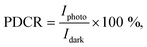
A metal–semiconductor–metal (MSM) PD was fabricated to examine the optoelectrical properties of the PE-MAC-etched α-Ga2O3 epilayer. Mesa-patterned Pt was defined on an unintentionally doped α-Ga2O3 layer grown by HVPE on a sapphire substrate to electrically isolate the active region at room temperature. The mesa-patterned Pt was removed by using aqua regia (35 °C, 30 min) solution, and interdigitated patterns were defined on the active area using e-beam lithography (MIRA3, TESCAN). Pt/Au (20/80 nm) interdigitated electrodes (IDTs) were deposited via e-beam evaporation to obtain the α-Ga2O3 MSM PD. The opto-electrical properties of the UV PD were measured using a semiconductor parameter analyzer (4155C, Agilent) connected to a low-vacuum probe station (MS TECH, 760 mmHg) under 254 nm UV irradiation (VL-6LC, Vilber Lourmat). A function generator (33250A, Agilent) and a shutter (SHB1T, Thorlabs) were utilized to control the UV irradiation time on the fabricated α-Ga2O3 MSM PD to obtain the time-dependent photoresponse characteristics.
Results and discussion
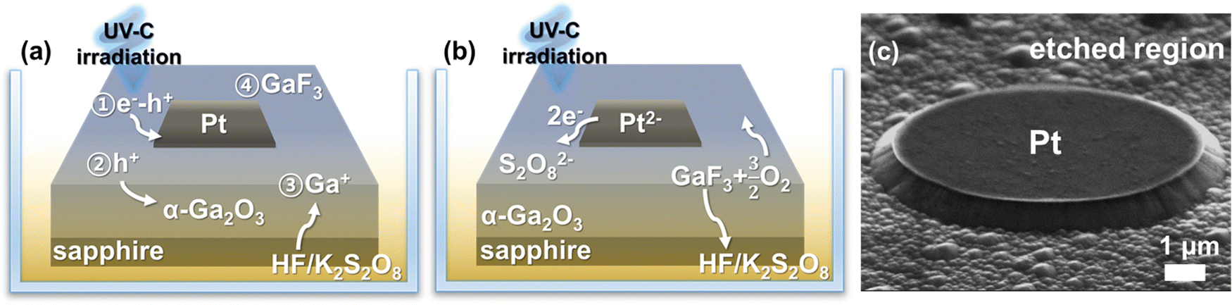
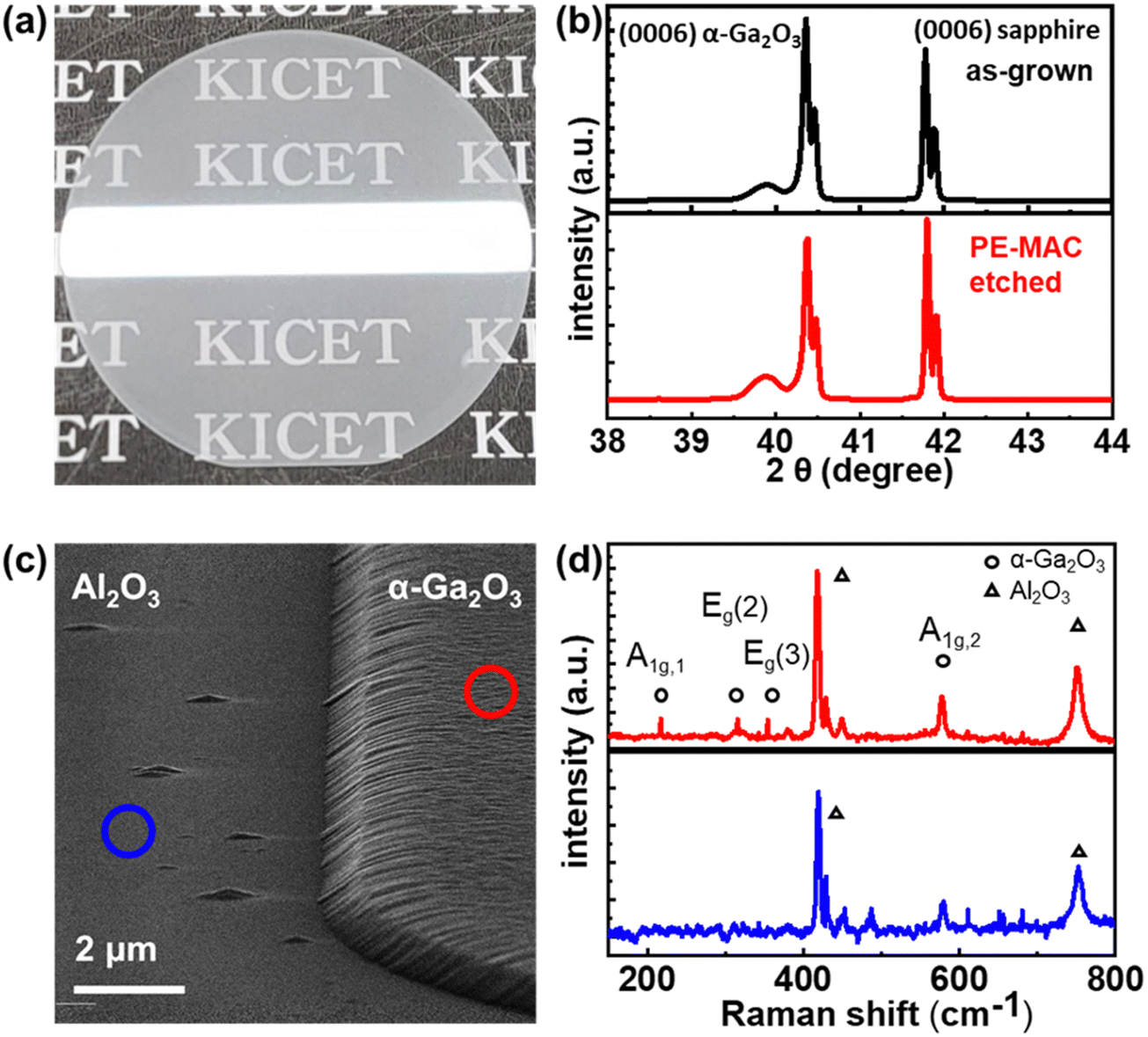
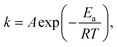
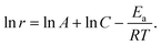
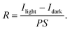
The mechanism of the PE-MAC etching of α-Ga2O3 is illustrated in Fig. 1. Fig. 1(a) shows the Pt-patterned α-Ga2O3 epilayer is irradiated with 185 nm UV light to generate EHPs in the surface. Then, the photogenerated electrons move to Pt with a high work function of 5.12–5.93 eV, making the holes accumulate on the surface of α-Ga2O3, where the holes react with gallium to generate gallium ions (Ga+), and gallium fluoride (GaF3) is finally generated through the reaction between Ga+ and HF. Fig. 1(b) shows the re-oxidation of the Pt2− that was reduced in the process shown in Fig. 1(a). The re-oxidation of Pt2− reduced by accepting electrons from α-Ga2O3 occurs by potassium persulfate (K2S2O8) in the etchant, where K2S2O8 is present as peroxydisulfate (S2O82−). S2O82− is decomposed into sulfate radicals (SO4˙−) when irradiated with UV light of wavelength under 300 nm. Because GaF3 was dissolved in HF, this etching process leads to the formation of a deep etched structure. If the Pt contact is unnecessary, it can be removed by using the aqua regia (35 °C, 30 min) solution. Because the metal-free area is selectively etched, this process is also called inverse-MAC etch. Fig. 1(c) shows the SEM images of α-Ga2O3 after PE-MAC etching. The surface of the etched region exhibits bumpy texture, which can be attributed to the disclosure of various facets of α-Ga2O3.24 A photograph of α-Ga2O3 grown by HVPE on a two-inch c-plane sapphire substrate is shown in Fig. 2(a). HR-XRD measurements revealed that the characteristic XRD peaks of the α-Ga2O3 epitaxial layer and the sapphire substrate appear at 40.12° and 41.56°, respectively, corresponding to the (0006) plane of α-Ga2O3 and (0006) plane of the c-plane sapphire in Fig. 2(b). The full width at half maximum (FWHM) of the α-Ga2O3 layer at 40.38° (2θ) peak slightly decreased from 209 (as-grown) arcsec to 202 arcsec (PE-MAC etched for 30 min), indicating that this process can be used to remove the defective sites. Grain size (D) can be estimated by using the following equation: D = 0.9λ/{FWHM × cos(θ)}, where D of the as-grown and the PE-MAC etched α-Ga2O3 were 146.0 nm and 151.2 nm, respectively. The complete removal of the Pt electrodes using aqua regia was confirmed by field-emission scanning electron microscopy, as shown in Fig. 2(c). Micro-Raman spectroscopy, shown in Fig. 2(d), was performed in each area of the blue and red circles in Fig. 2(c). The Raman modes of α-Ga2O3 that were absent in the blue-circled area were observed in the red-circled area, indicating that the PE-MAC etching process removed the entire α-Ga2O3 layer until the underlying sapphire substrate, which can act as an etch-stop layer.
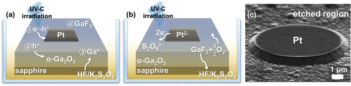 |
| | Fig. 1 Schematics of the PE-MAC etching process. (a) Formation of GaF3 upon UV irradiation and Pt reduction. (b) Oxidation of Pt2− by the oxidant (K2S2O8) and dissolution of GaF3 in HF. (c) Morphology of α-Ga2O3 after PE-MAC etching. | |
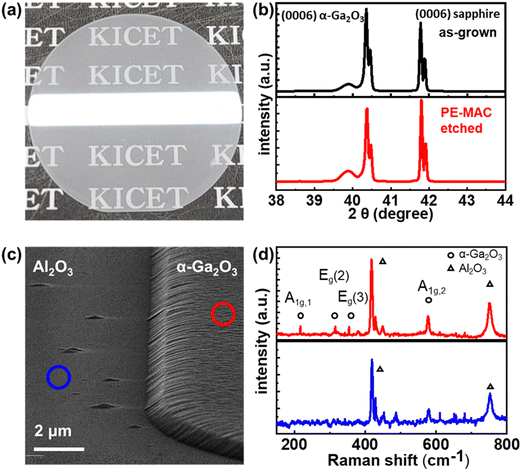 |
| | Fig. 2 (a) Photograph of the α-Ga2O3 epilayer on a two-inch sapphire substrate. (b) XRD patterns of the α-Ga2O3 epilayer on a sapphire substrate. (c) SEM image of PE-MAC-etched α-Ga2O3. (d) Raman spectrum of α-Ga2O3/sapphire (red) and sapphire (blue). | |
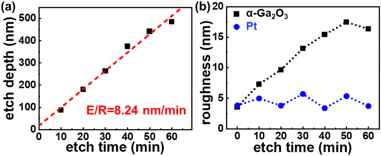
Fig. 3 shows the data for the PE-MAC etching of α-Ga2O3 in intervals of 10 min up to 60 min at room temperature (22 °C). The etch depth increased linearly with time, yielding an etching rate of 8.24 nm min−1. This rate is approximately five times higher than that (2 nm min−1) obtained at PE-MAC etching of β-Ga2O3 at room temperature, which can be attributed to the higher concentrations of the oxidants (from 0.18 (β-Ga2O3) to 1.5 mM (α-Ga2O3)) and the difference in the UV light wavelength (from 254 (β-Ga2O3) to 185 nm (α-Ga2O3)). The linearity of the extent of reaction with time and the relatively high etching rate at room temperature make the PE-MAC etching process compatible with a standard device fabrication process. The surface roughness of α-Ga2O3 increases linearly as etching progresses as shown in Fig. 3(b), saturating when the etching is completed at the smooth sapphire substrate. By sharp contrast, there is no correlation between the progress of etching and the surface roughness of the Pt electrode, indicating that the Pt electrode, which acts as a catalyst, does not directly participate in the etch reaction. As shown in Fig. 4(c), the Pt electrode was intact after the PE-MAC etch, implying that the underlying layer was completely protected from the etch. This is a great advantage over the conventional dry etch because the high-energy particles in the plasma etch can generate the defective sites even in the photoresist-covered region owing to its incomplete coverage.25 The root mean squared (RMS) roughness of the α-Ga2O3 surface was observed to increase by 2.8 nm per 100 nm of etching, which is similar to the roughness change observed during conventional plasma etching (ICP).13
 |
| | Fig. 3 (a) PE-MAC etching rate of α-Ga2O3 at room temperature (22 °C). (b) RMS roughness measured in a 10 × 10 μm2 area with the progress of etching. | |
 |
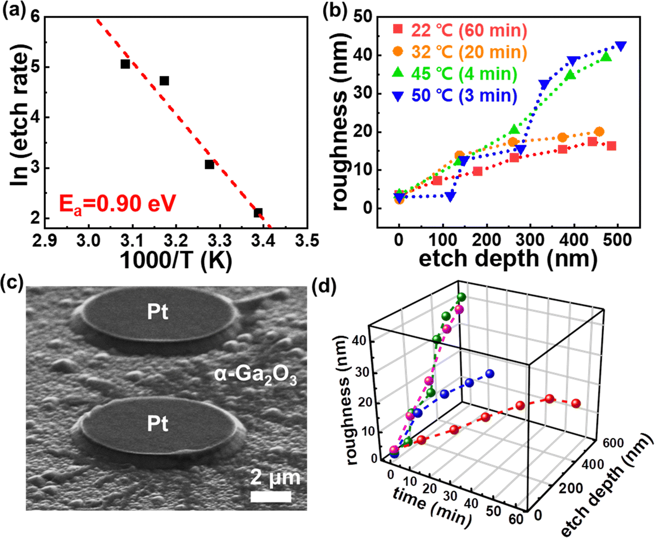
| | Fig. 4 (a) Arrehenius plot of the PE-MAC etching rate of α-Ga2O3. (b) Changes in RMS roughness by etch step was measured at 10 × 10 μm2 and various temperatures. (c) Surface morphology of α-Ga2O3 after PE-MAC etched at 50 °C for 3 min. (d) Dependence of the roughness on time and etching depth for each temperature condition. | |
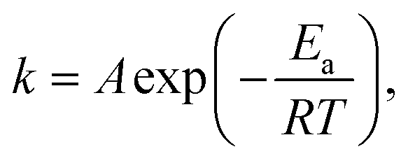
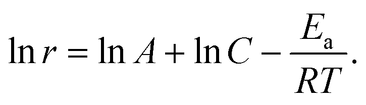
Wet etching involves the (1) surface diffusion of the etchant, (2) chemical reaction between the etchant and exposed surface, and (3) removal of reaction products by etching.26,27 The etching reaction rate, which depends on the diffusion rate or reaction rate, can be controlled by manipulating the process parameters. At the temperature that is comparable to the effective activation energy, the diffusion rate of a substance is slower than the rate of chemical reaction; hence, the overall reaction rate is determined by diffusion and is called a diffusion-controlled reaction. Under low-temperature conditions, the rate of the chemical reaction is slower than that of mass diffusion, and the overall reaction rate is determined by the rate of the chemical reaction that is called an activation-controlled reaction.28 The temperature effect of the reaction was studied to assess the mechanism of PE-MAC etching for α-Ga2O3 (Fig. 4) using the following equation:
| |  | (1) |
where
k is a function of the reaction constant,
Ea is the activation energy, and
A is a pre-exponential factor. The etching rate (
r) is expressed as
k ×
C, where
C is the molar concentration of the etchant. Assuming that the number of atoms present on the surface of α-Ga
2O
3 is constant,
r can be expressed as
| |  | (2) |
As shown in
Fig. 4(a), a high activation energy of 0.90 eV was obtained, indicating that this reaction is activation-controlled.
29,30 In the case of a diffusion-limited reaction, the etching species would react without being saturated on all surfaces of the target, resulting in poor reaction uniformity. Instead, the etchant is saturated on the entire surface of the target in the activation-controlled reactions, which allows a uniform reaction throughout the surface of Ga
2O
3.
Fig. 4(b) demonstrates that the surface roughness increases with increasing PE-MAC etching temperature from 22 to 50 °C, where the duration of the etch process is different because of the limitation in the film thickness. The SEM image in
Fig. 4(c) shows the growth domain in the α-Ga
2O
3 epilayer, where the Pt electrode is intact. The tilted sidewall around the Pt electrode can be explained by the depletion region formed between the Pt contact and α-Ga
2O
3. The dependence of the roughness on time and etching depth for each temperature condition is shown in
Fig. 4(d). The surface roughness increases exponentially with the increase in temperature, which is a similar trend to that observed for the etching rate. RMS roughness exhibits a rapid increase during etching at high temperatures. To achieve smooth surface at high-temperature PE-MAC etch, it is necessary to optimize the process conditions that increase the number of EHPs by increasing the UV intensity, reducing the spacing of the metal catalyst, and increasing the oxidant concentration.
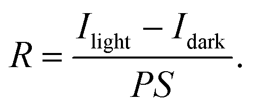
An α-Ga2O3-based UV-C MSM PD was fabricated by employing the PE-MAC etching process (Fig. 5). The UV absorber layer (α-Ga2O3) grown on the sapphire substrate was electrically isolated by PE-MAC etching. The current–voltage (I–V) curves of the MSM PD in the dark and under 254 nm UV irradiation were compared, as shown in Fig. 5(c). At a forward bias of +5 V, the currents obtained in the light and dark states (Ilight and Idark) are 0.43 nA and 90.6 pA, respectively. The responsivity (R), which is defined as the photocurrent normalized by the effective area and power of the incident light, is calculated as
| |  | (3) |
Here,
P is the illumination power and
S is the area of the light-receiving part (effective area). Thus,
R = 2.2 × 10
−2 A W
−1 was obtained using the above equation. The detectivity (
D*) represents the signal-to-noise ratio and is expressed as
| | 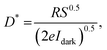 | (4) |
where
S is the effective area and
e is the charge of an electron. The photo-to-dark current ratio (PDCR), which represents the sensitivity of the PD, was estimated to be 4.73 × 10
5% using the following equation:
| |  | (5) |
where,
Iphoto is expressed as
Ilight −
Idark. The photoresponse characteristics of the fabricated MSM PD are summarized in
Table 1, which indicates the high performance of our MSM PD fabricated by the PE-MAC etching. The time-dependent photoresponse characteristics were obtained
via repetitive on/off cycles under these conditions (
Fig. 5(d)). They exhibited stable and reproducible photoresponse characteristics without persistent photocurrent (PPC), which is generally observed in an oxide-based photodevice owing to the defective sites such as oxygen vacancies. J. Bae
et al. reported the PPC effects in an α-Ga
2O
3-based MSM PD because the mid-gap state in α-Ga
2O
3 makes it active to UVB/A regions.
31 In our experiments, the rejection ratio (2.4 × 10
2), calculated as
R254nm/
R365nm, indicates that few mid-gap states existed in α-Ga
2O
3 after PE-MAC etching. The on/off cycles shown in
Fig. 5(d) are plotted as a bi-exponential function to obtain the rise and decay time constants (
Fig. 6). The bi-exponential function is given by
| | | I(t) = I0 + Ae−t/τ1 + Be−t/τ2. | (6) |
Here,
I0 is the dark current,
A and
B are constants, and
τ1 and
τ2 are time constants.
32 The time constants in the rise domain were
τr1 = 0.70 s and
τr2 = 1.97 s, and those in the decay domain were
τd1 = 0.03 s and
τd2 = 0.83 s. The rise/decay time constants of the UV-C MSM PD fabricated using PE-MAC etching were compared with the results reported in β-Ga
2O
3-based PD fabricated using conventional SF
6-based plasma etching methods, which employed a capacitively induced plasma etcher operating at 150 W and 13.56 MHz.
33 The PE-MAC-etched PD recorded notably lower
τ1 and
τ2, linked to intrinsic band-to-band transitions and slow reactions related to surface oxygen species or defects, respectively.
5,34 The decrease was significant in
τ2 than
τ1 in both rise and decay. Significantly lower
τ2 implies a significant reduction in plasma-induced damage with PE-MAC etching compared with conventional plasma etching. We also confirmed the electrical isolation by comparing the current of the active region and the current at adjacent electrodes. For further analysis of the defects in the fabricated UV PD, we investigated the spectral selectivity, which is shown in
Fig. 5(c); this figure also demonstrates that the electrical isolation by the PE-MAC etching is extremely effective because the isolation currents between the active layer are nominal even under UV-C illumination. Our PE-MAC etching maintained the solar-blind characteristics of α-Ga
2O
3 without creating a mid-gap state while achieving electrical isolation. The PE-MAC etching, which enables rapid etching at room temperature while maintaining crystallinity, is a highly promising technique for the fabrication of optoelectronic/electronic devices to exploit the potential of α-Ga
2O
3.
 |
| | Fig. 5 (a) Schematic of the metal–semiconductor–metal photodetector (MSM PD) fabrication process. (b) The optical-microscope image of the produced PD. (c) I–V characteristics of the PD and isolated current under 254 nm UV irradiation/dark condition. (d) Time-dependent photoresponse characteristics of the fabricated MSM PD under 254 and 365 nm UV irradiations. | |
Table 1 Photoresponse parameters of the MSM PD under 254 nm UV irradiation (power density: 2.8 W m−2; bias: 5 V)
| Wavelength (nm) |
R (A W−1) |
D* (Jones) |
PDCR (%) |
Rise time (s) |
Decay time (s) |
| 254 (UV-C) |
0.017 |
2.6 × 10⁹ |
3.53 × 10⁴ |
0.34/1.2 |
0.07/0.07 |
| 365 (UV-A) |
7.0 × 10⁻⁵ |
1.0 × 10⁷ |
2.7 × 10² |
0.16/3.3 |
0.12/1.6 |
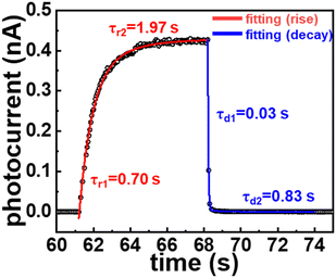 |
| | Fig. 6 Bi-exponential curve fitting of photoresponse to irradiation with 254 nm UV light. | |
Conclusion
We identified the mechanism of PE-MAC etching by applying it to a HVPE-grown α-Ga2O3 epilayer, and achieved stable, damage-free, and highly anisotropic wet etching. We also evaluated the performance of this technique by fabricating electrically isolated MSM PD devices by PE-MAC etching and demonstrated anisotropic etching by irradiating the sample with a short-wavelength light source to generate EHPs, using patterned Pt metal catalysts to withdraw electrons. The patterned Pt metal remained intact and could be removed when necessary. PE-MAC etching yielded an etching rate of 8.24 nm min−1 at room temperature with a smooth sidewall, and the reaction progress increased linearly with time. An activation energy of 0.90 eV (86.7 kJ mol−1) was obtained from the Arrhenius plot of the etching rates at various temperatures. The linearity of the extent of reaction over time, high activation energy, and rapid increase in the etching rate with increase in temperature indicate that the PE-MAC etching of α-Ga2O3 is an activation-controlled reaction. The reaction mechanism is governed by an activation-controlled reaction, and the observed etching rate of several nanometers per minute at room temperature makes PE-MAC etching a promising method for electronic device fabrication. Time-dependent photoresponse characteristics from the MSM PD devices electrically isolated by PE-MAC etching were considerably improved; this confirmed that PE-MAC etching is a damage-free removal process that maintains crystal quality. The simplicity and vacuum-plasma-free characteristics of PE-MAC etching, as well as its high etching rate at room temperature and ability to prevent the formation of defects, indicate that it is a viable method for manufacturing electronic and optical devices based on α-Ga2O3.
Author contributions
Woong Choi – experiments, data analysis and writing. Dae-Woo Jeon – sample preparation, review and editing. Ji-Hyeon Park – sample preparation, review and editing. Dongryul Lee – data curation, methodology, review and editing. Soobeen Lee – investigation, data curation and review. Kwang Hyeon Baik – review and editing. Jihyun Kim – supervision, conceptualization, writing, review and editing.
Conflicts of interest
There is no conflict to declare.
Acknowledgements
This work was supported by Korea Institute for Advancement of Technology (KIAT) grant funded by the Korea Government (P0012451, The Competency Development Program for Industry Specialist), K-Sensor Development Program (RS-2022-00154729) funded by the Ministry of Trade, Industry and Energy (MOTIE, Korea), and Korea Research Institute for defense Technology planning and advancement (KRIT) – Grant funded by Defense Acquisition Program Administration (DAPA) (KRIT-CT-22-046).
References
- E. Ahmadi and Y. Oshima, J. Appl. Phys., 2019, 126, 160901 CrossRef.
- N. S. Jamwal and A. Kiani, Nanomaterials, 2022, 12, 2061 CrossRef CAS PubMed.
- S. J. Pearton, J. Yang, P. H. Cary, F. Ren, J. Kim, M. J. Tadjer and M. A. Mastro, Appl. Phys. Rev., 2018, 5, 011301 Search PubMed.
- C. Yang, H. Liang, Z. Zhang, X. Xia, P. Tao, Y. Chen, H. Zhang, R. Shen, Y. Luo and G. Du, RSC Adv., 2018, 8, 6341 RSC.
- J. Kim, S. Oh, J. Kim, F. Ren and S. J. Pearton, J. Mater. Chem. C, 2016, 4, 9245 RSC.
- H. Son and D. W. Jeon, J. Alloys Compd., 2019, 773, 631 CrossRef CAS.
- H. Ito, K. Kaneko and S. Fujitaice, Jpn. J. Appl. Phys., 2012, 51, 100207 CrossRef.
- B. J. Baliga, IEEE Electron Dev. Lett., 1989, 10, 455 Search PubMed.
- N. Allen, M. Xiao, X. Yan, K. Sasaki, M. J. Tadjer, J. Ma, R. Zhang, H. Wang and Y. Zhang, IEEE Electron Device Lett., 2019, 40, 1399 CAS.
- C. W. Tsou, K. P. Wei, Y. W. Lian and S. S. H. Hsu, IEEE Electron Device Lett., 2016, 37, 70 CAS.
- L. Cheng, J. Y. Yang and W. Zheng, ACS Appl. Electron. Mater., 2022, 4, 4140 CrossRef CAS.
- H. Okumura and T. Tanaka, Jpn. J. Appl. Phys., 2019, 58, 120902 CrossRef CAS.
- Z. Jian, Y. Oshima, S. Wright, K. Owen and E. Ahmadi, Semicond. Sci. Technol., 2019, 34, 035006 CrossRef CAS.
- J. Yang, S. Ahn, F. Ren, R. Khanna, K. Bevlin, D. Geerpuram, S. J. Pearton and A. Kuramata, Appl. Phys. Lett., 2017, 110, 142101 CrossRef.
- S. J. Pearton, E. A. Douglas, R. J. Shul and F. Ren, J. Vac. Sci. Technol., A, 2020, 38, 020802 CrossRef CAS.
- Y. Yao, Y. Ishikawa and Y. Sugawara, Phys. Status Solidi A, 2020, 217, 2 CrossRef.
- B. S. Choi, J. H. Um, H. J. Eom, D. Jeon, S. Hwang and J. K. Kim, J. Korean Cryst. Growth Cryst. Technol., 2022, 32, 40 Search PubMed.
- Y. Zhang, A. Mauze and J. S. Speck, Appl. Phys. Lett., 2019, 115, 013501 CrossRef.
- X. Li and P. W. Bonn, Appl. Phys. Lett., 2000, 77, 2572 CrossRef CAS.
- X. Li and Curr Opin, Solid State Mater. Sci., 2012, 16, 71 CrossRef CAS.
- W. Chern, K. Hsu, I. S. Chun, B. P. D. Azeredo, N. Ahmed, K. H. Kim, J. M. Zuo, N. Fang, P. Ferreira and X. Li, Nano Lett., 2010, 10, 1582 CrossRef CAS PubMed.
- M. Dejarld, J. C. Shin, W. Chern, D. Chanda, K. Balasundaram, J. A. Rogers and X. Li, Nano Lett., 2011, 11, 5259 CrossRef CAS PubMed.
- H. Asoh, T. Yokoyama and S. Ono, Jpn. J. Appl. Phys., 2010, 49, 0465051 CrossRef.
- S. Shapenkov, O. Vyvenko, V. Nikolaev, S. Stepanov, A. Pechnikov, M. Scheglov and G. Varygin, Phys. Status Solidi B, 2022, 259, 2100598 CrossRef.
- A. N. Noemaun, F. W. Mont, J. Cho, E. F. Schubert, G. B. Kim and C. Sone, J. Vac. Sci. Technol. A, 2011, 29, 051302 CrossRef.
- Z. Jin, Y. Liu, N. Xia, X. Guo, Z. Hong, H. Zhang and D. Yang, CrystEngComm, 2022, 24, 1127 RSC.
- S. Ohira and N. Arai, Phys. Status Solidi C, 2008, 5, 3116 CrossRef CAS.
- T. Oshima, T. Okuno, N. Arai, Y. Kobayashi and S. Fujita, Jpn. J. Appl. Phys., 2009, 48, 040208 CrossRef.
- Y. H. Choi, K. H. Baik, S. Kim and J. Kim, Appl. Surf. Sci., 2021, 539, 148130 CrossRef CAS.
- Y. H. Choi, K. H. Baik, R. Choi, J. Oh and J. Kim, ECS J. Solid State Sci. Technol., 2019, 8, N42 CrossRef CAS.
- J. Bae, D.-W. Jeon, J. H. Park and J. Kim, J. Vac. Sci. Technol., A, 2021, 39, 033410 CrossRef CAS.
- A. Kim, G. Lee and J. Kim, J. Vac. Sci. Technol., A, 2021, 39, 053412 CrossRef CAS.
- Y. Kwon, G. Lee, S. Oh, J. Kim, S. J. Pearton and F. Ren, Appl. Phys. Lett., 2017, 110, 131901 CrossRef.
- J. Yu, J. Lou, Z. Wang, S. Ji, J. Chen, M. Yu, B. Peng, Y. Hu, L. Yuan, Y. Zhang and R. Jia, J. Alloys Compd., 2021, 872, 159508 CrossRef CAS.
Footnote |
| † Electronic supplementary information (ESI) available: The data of PE-MAC etching are shown in Fig. S1 (32, 45, and 50 °C). Fig. S2 shows the I–V characteristics of α-Ga2O3 PD under dark condition as well as 254 and 365 nm lights illuminations. See DOI: https://doi.org/10.1039/d3ma00424d |
|
| This journal is © The Royal Society of Chemistry 2023 |
Click here to see how this site uses Cookies. View our privacy policy here. 
 Open Access Article
 This Open Access Article is licensed under a Creative Commons Attribution-Non Commercial 3.0 Unported Licence
 a,
Dae-Woo
Jeon
b,
Ji-Hyeon
Park
b,
Dongryul
Lee
a,
Dae-Woo
Jeon
b,
Ji-Hyeon
Park
b,
Dongryul
Lee