DOI:
10.1039/D3MA00398A
(Paper)
Mater. Adv., 2023,
4, 4204-4215
A first-principles study of the electronic, optical, and transport properties of novel transition-metal dichalcogenides
Received
12th July 2023
, Accepted 15th August 2023
First published on 15th August 2023
Abstract
Transition-metal dichalcogenides have great potential to be used as photoconductors and in optoelectronic devices. Using density functional theory calculations, we investigated the electronic, structural, optical, and thermoelectric properties of tungsten-based novel dichalcogenide materials. The electronic band profiles well support the density of states, confirming the semiconducting nature of the examined materials. The formation energies are calculated to predict the stability of these materials and the cohesive energies are also computed. Additionally, optical constants including the components of complex dielectric functions, energy loss functions, absorption coefficients, refractive indexes, reflectivity, extinction coefficients, and the real parts of optical conductivity were computed and explicated for their potential application in optoelectronic devices. The significant thermoelectric parameters were also predicted and the obtained outcomes were discussed, signifying that the materials are appropriate for thermoelectric applications. Primarily, this current study could help the development of distinct and potential semiconducting devices and their applications.
1. Introduction
Transition metal dichalcogenides (TMDCs) have many potential uses especially in solar energy harvesters and some other high technological optoelectronic devices.1–5 The possible employment of these materials has drawn the interest of many researchers during the last few years. These TMDCs have a variety of two-dimensional (2D) structures reliant on selecting a chalcogen and transition metal, including Mott insulators,6 metals,7–9 charging density wave systems,10,11 superconductors,12 and semiconducting materials.13 Semiconducting TMDCs such as, MoS2, MoSe2, MoTe2, TcS2, TcSe2, TcTe2, TSi2, HfS2, and HfSe2, are considered potential candidates for a variety of applications.14 The materials from the family have intriguing and technologically advantageous features, particularly their two-dimensional (2D) counterparts.15,16 The materials with the formula MZ2, where M stands for transition metals and Z for chalcogen, can either be metals or semiconductors with direct or indirect band gaps, depending on their stoichiometry. To accurately reproduce the description of electronic properties, these materials have been investigated using a variety of techniques and approximations. Wilson and Yoffe17 have evaluated the electronic characteristics of the ZrS2 material. The same material was predicted as a semiconductor with an indirect band gap of 1.68 eV, according to a study by Greenway and Nitsche.18 They also investigated the optical absorption over the energy range of 0.05–2.5 eV. Materials such as ZrSe2 have an indirect band gap of 1.2 eV, according to Lee et al.19 Similarly, Bell and Liang20 used the Kramers–Kronig analysis to determine the frequency-dependent complex dielectric function and associated optical properties from the energy loss data of ZrS2 for electric field vector Ec. For the same electric vector Ec, Hughes et al.21 studied the reflectance spectra of ZrS2 and ZrSe2 in the photon energy range from 4.5 to 14 eV. Besides this, Bayliss and Liang22 studied the reflectivity of ZrS2 over the energy range of 0.5–5.0 eV, and they discovered a significant polarization dependency. In the production of third generation solar cells, materials having band gaps in this range are promising. For application in rechargeable batteries, cathodes can be produced using their chain-like layered nature.23 The structural, electrical, and optical characteristics of TcS2, TcSe2, and TcTe2 were theoretically explored using appropriate van der Waals corrections, and the post-DFT techniques such as the GW method were used for correcting the DFT-predicted band gap errors.24
The tight binding linear muffin-tin orbitals (FP-LMTOs), used by Kalpana et al.,25 were employed to examine the structural and electrical characteristics of materials from the family. Fleszar and Hanke26 have studied the electronic excitations of these TMDCs using an ab initio GW-approach. To the best of our knowledge, theoretical data have been presented by J. Wang et al.,27 who reported the electronic and optical properties of tungsten-based binary dichalcogenide monolayers under biaxial strain employing conventional local density approximation and GGA as the exchange–correlation functional. The structures are layered, though, and it has been noted that traditional GGA functions were unable to accurately predict or describe the structural features of the layered systems.28 For an accurate representation of the structural features of WS2, WSe2, and WTe2, on which the materials’ electronic characteristics depend, long-term dispersive forces were crucial components. The band gap of semiconductors is also known to be 10–40% underestimated using PBE and LDA techniques. Given the potential use of these materials in the fabrication of third generation solar energy photovoltaic converters, it is surprising that knowledge is scarce. The materials from the family have semiconductor properties and their DFT band gaps fall mostly in between 0.3 and 1.0 eV.29 In this study, we explored the structural, electronic, optical, and thermoelectric properties of WS2, WSe2, and WTe2 compounds using the Kohn–Sham density functional theory approach. We calculate their electronic properties using the modified Becke–Johnson potential to finely understand their electronic nature. We solve the Bethe–Salpeter equation (BSE)30 to determine their optical characteristics. The mBJ approximation is thought to be the most up-to-date first principles technique for accurately modeling semiconductor band gaps with a degree of precision comparable to experiments with an accuracy of 10%. Due to the scarcity of data for electronic, optical, and thermoelectric properties, and for their usage in optoelectronic, and thermoelectric applications, certain WZ2 (Z = S, Se, and Te) caught our attention. This paper is organized as follows: in the 2nd section, we describe the methodology used in the computation. In the 3rd section, we present the results and discussion. In the 4th section, the obtained results were presented.
2. Computational details
The structure, electronic, optical, and thermoelectric properties of tungsten-based binary WZ2 (Z = S, Se, and Te) chalcogenides have been studied with first principles computation that is based on density functional theory.31 The WIEN2k code,32 which employs the full-potential linearized augmented plane wave technique, is used to conduct the studies. The generalized gradient approximation PBE-GGA scheme33 is used to characterize the exchange correlation potentials. In DFT calculations, the choice of the exchange–correlation functional, such as PBE-GGA, is essential since it takes into consideration the effects of electron exchange and correlation. Due to their distinguished nature, electrons interact and this is described by the exchange term, whereas the correlation term takes into consideration the repulsion between electrons. The TB-mBJ potential, which incorporates a modified Becke–Johnson potential, adds a self-interaction correction to the exchange–correlation function and addresses this problem. For precisely estimating the electronic properties like band gaps, this adjustment aids in capturing the appropriate energy gap between the occupied and unoccupied states. It has been demonstrated that a variety of materials, including semiconductors, transition metal oxides, and materials with significant spin–orbit coupling, perform better when the TB-mBJ potential is used. It can more precisely predict the electronic structure characteristics, such as band alignments and band gaps, as well as better replicate experimental characteristics, such as lattice constants and formation energies. To increase the precision of the computations for the electronic band gap in the present work, the TB-mBJ potential34 was employed. The electronic states are expanded using the spherical harmonic inside the atomic spheres having angular maximum number Lmax = 10. In the interstitial zones, the threshold for plane wave expansion is equal to RMT × Kmax = 7, where RMT is the smallest muffin-tin radius and Kmax is the largest wave vector. For cycles that are self-consistent, 0.0001 Ry is the convergence criteria. A k-mesh of 6 × 6 × 6 was used during the structural optimization process. For the calculations for the electronic characteristics, we used a denser 14 × 14 × 14 k-mesh.
We also investigated the linear response of the system to an external electromagnetic field using a frequency-dependent complex dielectric function. We add a transition from the occupied to the unoccupied orbital states in the first Brillouin zone (FBZ) using the following method to get the inter-band contributions to the imaginary component:35,36
| |  | (1) |
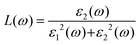
In the formula given, M stands for the dipole matrix, Ei stands for the energy of electron in the ith state, i and j stand for ith state's initial and final states, respectively, and fi is ith state's distribution function of Fermi energy. The letter ‘ω’ stands for the incident light's frequency, while the letter “k” stands for the wave vector of the electrons participating in the transition. We determine the real component, ε1(ω), of the dielectric function using the Kramers–Kronig relation:35,36
| |  | (2) |
The principal value and complex shift are represented by p in the equation above. These characteristics can be calculated using conventional equations:35,36
| |  | (3) |
| |  | (4) |
| |  | (5) |
| |  | (6) |
| |  | (7) |
The rigid-band method and the Boltzmann theory, which have successfully been used to estimate the thermoelectric properties of numerous materials for a decade, were used to compute the transport properties. The constant scattering time estimate was used to put this strategy into practice in the BoltzTrap code.
3. Results and discussion
3.1 Structural properties
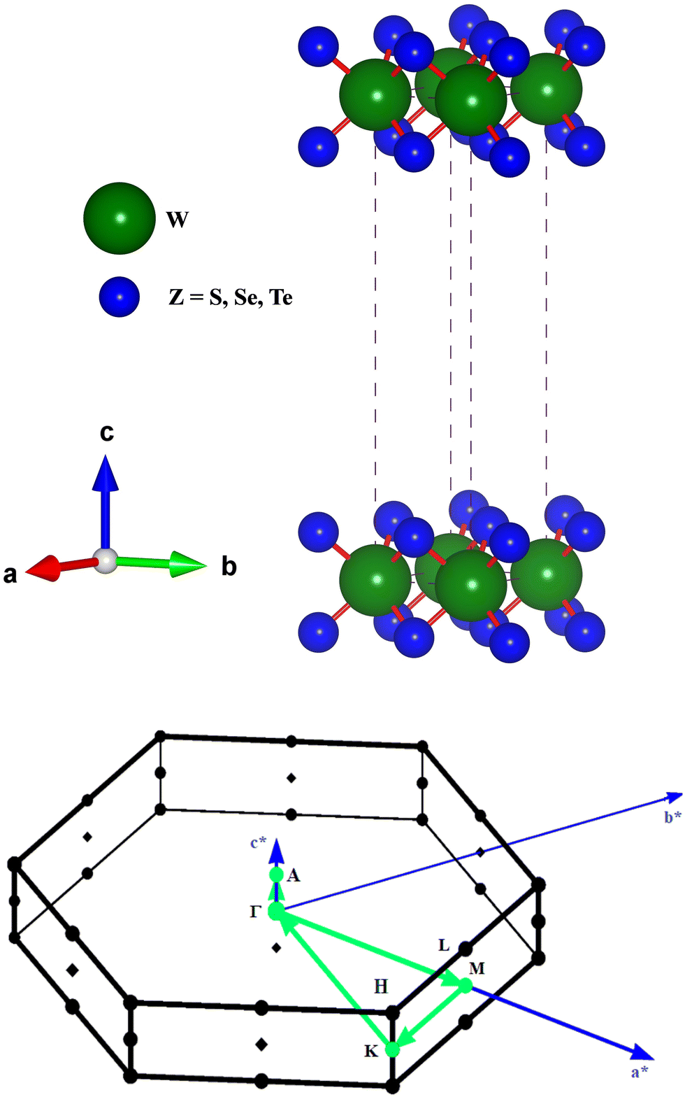
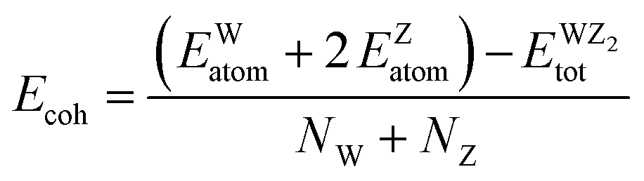
The hexagonal-type structure of tungsten-based WZ2 (W = S, Se, and Te) TMDC crystallizes with space group P63/mmc. The PBE-GGA and TB-mBJ approximations were used to perform the structural relaxation of these materials. To find the functional that will better forecast qualities, many functionals were tried. We relax the structures in the first stage by permitting changes in volume and atomic locations to estimate the equilibrium volume. The second stage involves creating thirteen distinct volumes inside the equilibrium-guessed volume, which is fixed, and the structure is relaxed by shifting the atomic locations. We derive cohesive energy from the various exchange correlations taken into account for the structures with various atomic volumes. The most advantageous volume of the structure is thought to be the one that has the lowest cohesive energy and it is from this volume that structural parameters are deduced. The computed unit cell structure is depicted in Fig. 1 together with the equilibrium structural features; the larger atoms in the illustration represent the metal. With an increase in the charge number of the chalcogen atoms, the formation and cohesive energies per atom decline in their magnitude, indicating the compounds to be relatively less stable. Phonon dispersion plots provide helpful knowledge regarding the lattice dynamics and material stability. These plots depict the link between the phonon frequency and the crystal lattice's wave vector. Stable materials feature a smooth and well-behaved phonon dispersion plot with no negative frequencies or imaginary modes.37,38 The CASTEP package,39 which also operates within the context of DFT, is used for obtaining the phonon dispersion plots of the materials under investigation as displayed in Fig. 2(a)–(c). The phonon dispersion calculations predicted and confirmed the studied materials’ stable nature. The results of our calculations conclusively show that the absence of negative frequencies proved that the material systems we examined have stable structures.
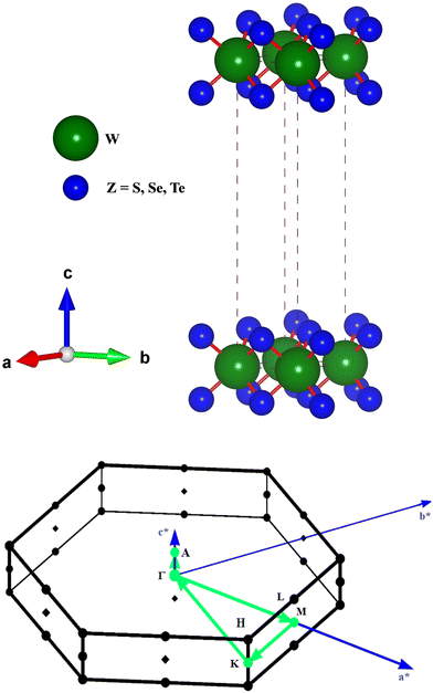 |
| | Fig. 1 The unit cell structure for WZ2 (Z = S, Se, and Te) materials and the BZ for the calculated band profiles. | |
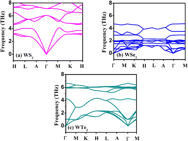 |
| | Fig. 2 The calculated phonon dispersion plots for the (a) WS2, (b) WSe2, and (c) WTe2 materials. | |
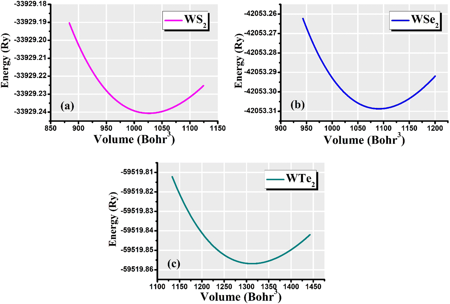
The volume of the unit cell of WZ2 (Z = S, Se, and Te) compounds was optimized with the goal of determining ground state parameters such as the lattice constants a, b, and c and the bulk modulus B. The stability of these investigated materials in their current structural phase is revealed by the energy vs. volume optimization curves shown in Fig. 3(a)–(c), which are obtained by analyzing the form of the curve and figuring out the volume at which the energy is minimized. The region of the curve where the total energy is the lowest is known as the equilibrium volume. The stability is confirmed by the energy vs. volume curve, which exhibits a negative curvature around the equilibrium volume. This occurs as a result that the material being pushed back towards the equilibrium volume by an increase in energy caused by each small volume deviation from the equilibrium volume. During the optimization phase, total energy values for different volumes of the unit cell were computed. Additionally, as a result, the volume and overall ground state energy increase, while the bulk modulus decreases. The predicted cohesive energy supports the conclusions obtained using the formula given below:40,41
| |  | (8) |
Here
NW and
Nz represent the number of W and Z atoms, respectively. The
EWatom and
EZatom values represent the energy of W and Z atoms, respectively.

signifies the bulk energy of the WZ
2 system.
40,41 To determine the total energies and the isolated free atoms in our work, we estimated the cohesive energies of WS
2, WSe
2, and WTe
2 using DFT calculations. The cohesive energy values for WS
2, WSe
2, and WTe
2 were determined to be 3.56 eV per atom, 3.82 eV per atom, and 4.15 eV per atom, respectively. According to these figures, WS has the strongest bonding of the three materials, while WTe
2 has the worst bonding. This conclusion is in line with the trend in the bulk modulus data, which was supported by the finding that WS is the material most resistant to external pressure:
40,41| | 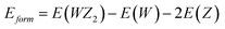 | (9) |
 |
| | Fig. 3 Total-energy vs. volume optimization for the (a) WS2, (b) WSe2, and (c) WTe2 materials. | |
For WS2, WSe2, and WTe2, the formation energies that were examined were −1.36, −1.42, and −1.75 (eV f. u.−1), respectively. These materials’ energies, which range from −1.3 to −3.0 eV f. u.−1 and are much lower than those of the equivalent elemental hull, attest their stability. Lower formation energies are linked to more ionic bonds, as shown by the strong correlation between this formation energy and the grade of ionicity between W–Z bonds. The convex hull, a model for formation energy as a function of composition, connects phases with lower formation energies than all other phases. The convex hull that is the closest to the compositions of interest is more reliable and connected to the formation energy values that we discovered.40,41
3.2 Electronic properties
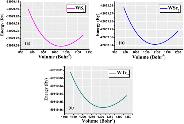
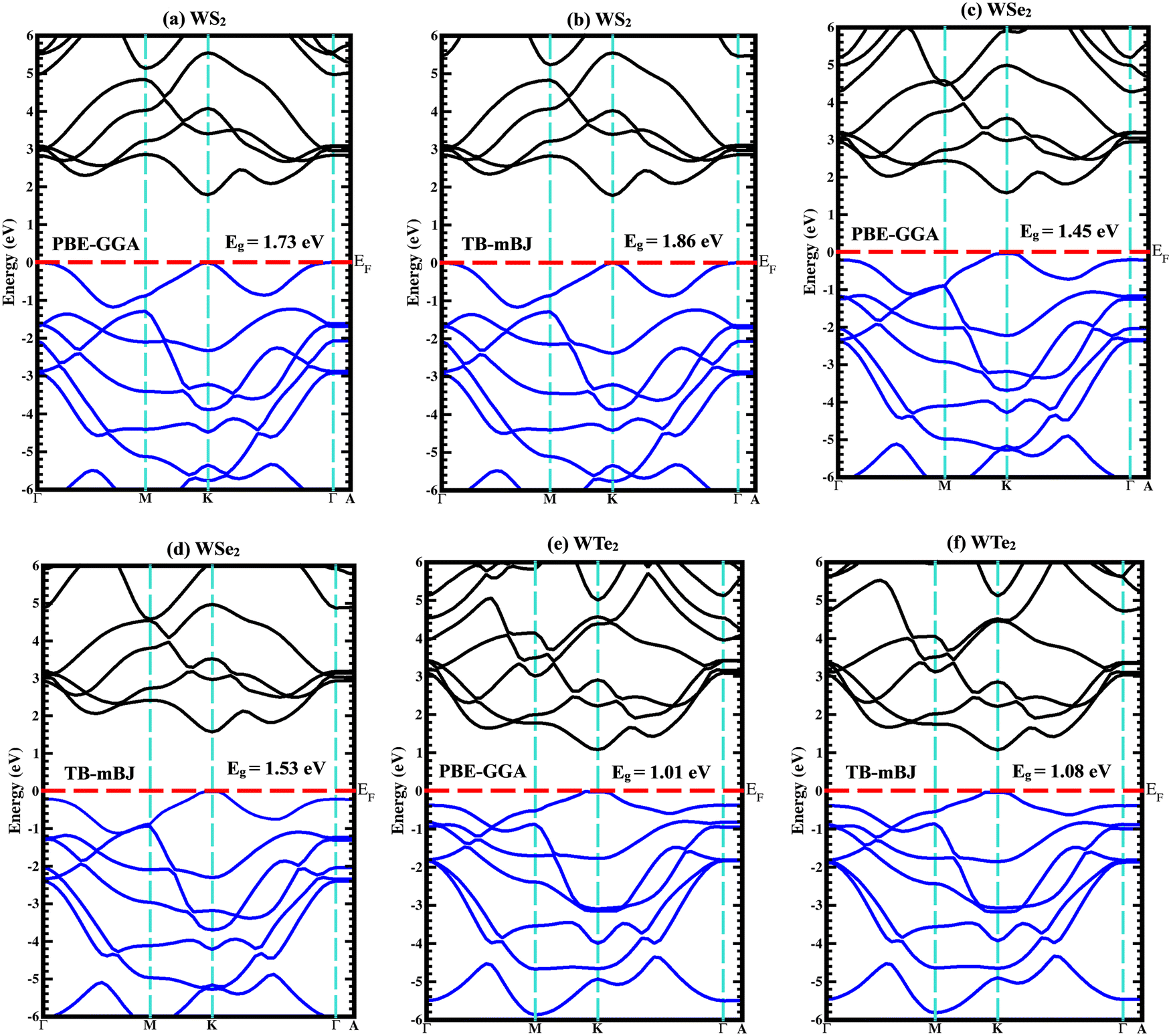
The majority of the physical characteristics of solid materials are influenced by the electronic band structure; as a result, understanding the electronic band structure is crucial. The energy band gap and its magnitude affect every semiconductor's optical and charge-transfer characteristics. Even though KS-DFT is particularly useful for predicting a material's properties in its ground state, it is unable to accurately describe a material's electronic properties. The Trans- and Blaha-modified Becke–Johnson potential (TB-mBJ) was used to determine the band gaps of the WZ2 (Z = S, Se, and Te) structures to improve band gap predictions. In the first Brillouin zone (BZ), the band structure is examined in a very symmetrical fashion. The extremely symmetric points in this instance are crucial points connected to a single primitive cell of the reciprocal lattice. The crystalline structure of the particular symmetry group determines the coordinates of highly symmetric points. The unit primitive cell and all of the unit vector coefficients are determined using the lattice parameters for both the real and reciprocal lattices. One tungsten and three chalcogenide (S, Se, and Te) atoms make up the unit cell. The band structure and density of states (DOS) of binary WZ2 (Z = S, Se, and Te) TMDCs have been investigated. Both the PBE-GGA and TB-mBJ band structures for these three materials are shown in Fig. 4(a)–(f) along with predicted band gap values. Although the PBE-GGA approach is well-liked and computationally effective, it may not offer precise band gap measurements, especially for insulating and semiconducting materials. TB-mBJ, on the other hand, is a more sophisticated technique that addresses the band gap underestimation problem and can produce better outcomes for materials with narrow band gaps and significant electronic state localization. The WS2 family of structures all are indirect band gap semiconductors with valence band maxima (VBM) and conduction band minima (CBM) positioned at different high symmetric points as illustrated in Fig. 4(a) and (b). The three compounds’ dominant orbital characteristics are comparable but not much identical. A semiconducting behavior with an indirect band gap of 1.86 eV was predicted for the WS2 material. The W-f and S-s orbitals are primarily responsible for the band formation in the 2.0 eV to 5.5 eV range in the conduction band and the 0 eV to −6.0 eV range in the valence band region. The WSe2 band structure is depicted in Fig. 4(c) and (d). WSe2 has an indirect band gap of 1.53 eV calculated by employing the TB-mBJ potential. The W-f and Se-p orbitals are primarily responsible for the band formation ranging from 1.91 to 5.0 eV in the conduction band and in the range of 0 to −6.0 eV in the valence band region. Similar results can be seen (Fig. 4(e) and (f)) for the WTe2 material, which also has an indirect band gap of 1.08 eV and the W-f and Te-p orbitals are primarily responsible for the band formation in the 1.5 eV to 4.5 eV range in the conduction band and in the 0 eV to −5.5 eV range in the valence band region. The band gaps are listed in the following order: the Eg for WS2 > WSe2 > WTe2, that is when the atomic number of these chalcogenide atoms surges, the electronic band gap narrows.
 |
| | Fig. 4 Calculated band structures using both PBE-GGA and TB-mBJ potentials for (a), (b) WS2, (c), (d) WSe2, and (e), (f) WTe2 materials. | |
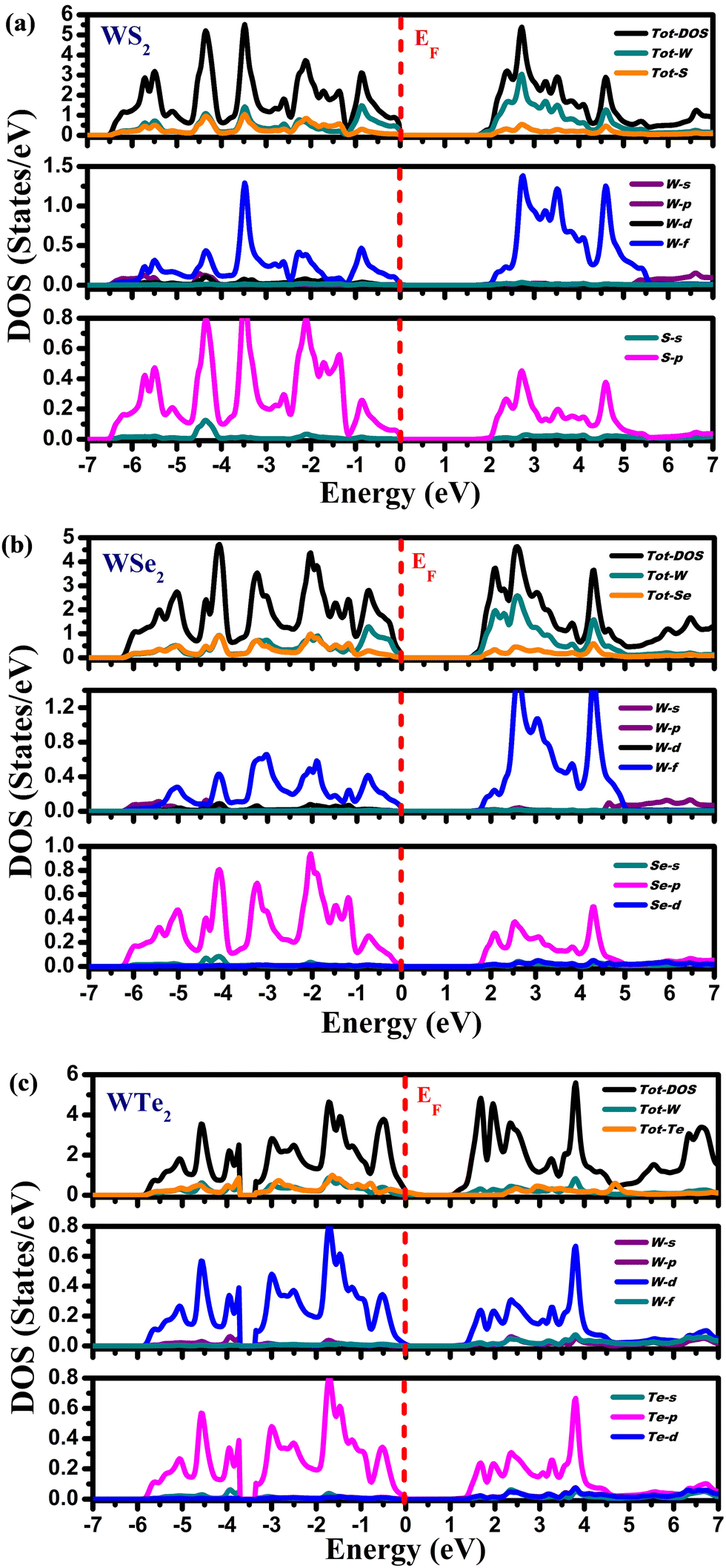
Fig. 5 depicts the partial (PDOS) and total density of states (TDOS). The computed density of states for these compounds exhibits a consistent pattern of behavior. Different energy states’ contributions to the valence and conduction bands are explained by these DOS calculations. The compounds exhibit semiconducting nature because the Fermi level divides the valence band (VB) and the conduction band (CB). According to Fig. 5(a), the Tot-W and Tot-S atoms contribute marginally to the valence band's energy range from 0.0 eV to −6.5 eV. The W-f and S-p states in PDOS play a significant role in this energy range. In the energy range from 2.0 eV to 5.5 eV, the Tot-W atom makes the largest contribution to the conduction band, whereas, in PDOS, the W-f and S-p states provide the largest contributions in this energy range. The Tot-W and Tot-Se have negligible contributions in the energy range from 0.0 eV to −6.5 eV in WSe2, as illustrated in Fig. 5(b). The W-f and Se-p states play a significant role in PDOS. The Tot-W makes the largest contribution in the energy range between 2.0 and 5.5 eV in the conduction band, and in PDOS, the W-f and Se-p states make the largest contributions. Similar to WTe2, from Fig. 5(c) the Tot-W and Tot-Te atoms provide a negligible contribution to the valence band ranging from 0.0 to −6.5 eV. The W-f and -p states of Te in the PDOS play a significant role in this energy range. Similarly, in the conduction band, the Tot-W state makes the largest contribution ranging from 2.0 to 5.5 eV, but in PDOS, W-f and Te-p states make the largest contributions in this energy range.
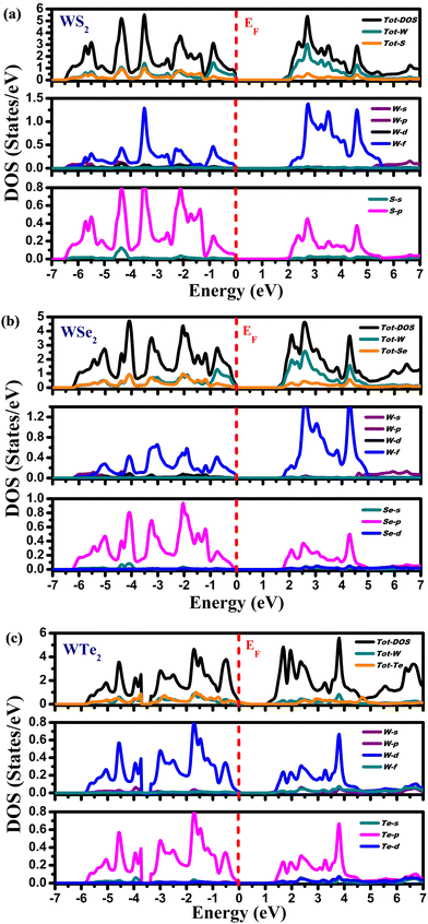 |
| | Fig. 5 The density of states for (a) WS2, (b) WSe2, and (c) WTe2 materials. | |
3.3 Optical properties
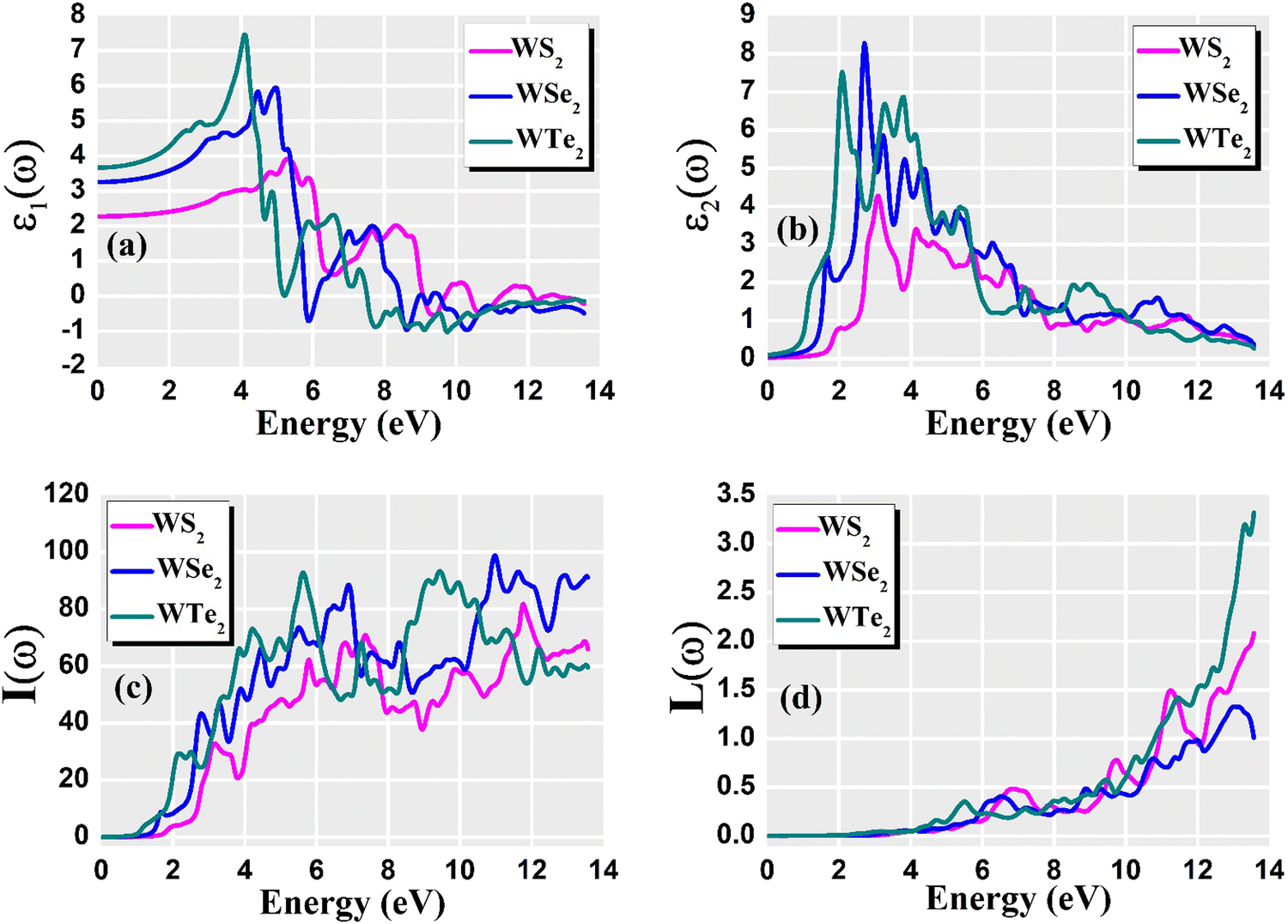
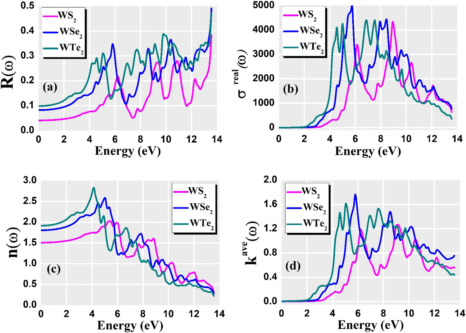
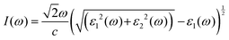
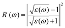
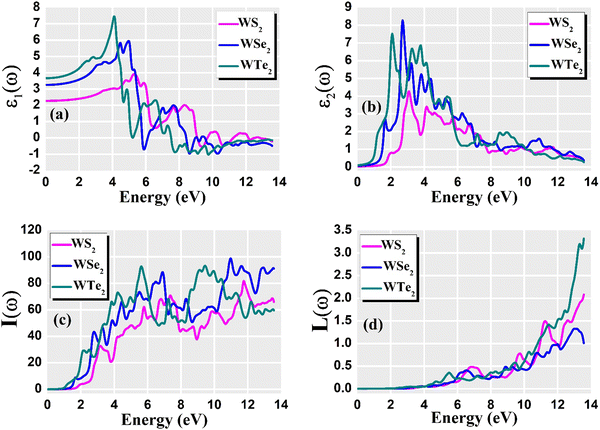
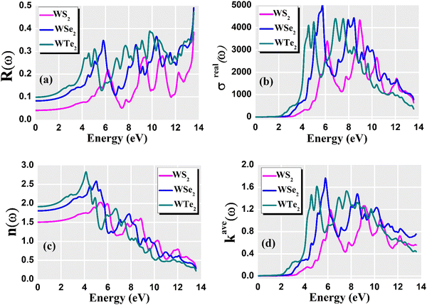
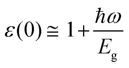
For optoelectronic device applications, optical dispersion abilities are crucial. The real and imaginary parts of the dielectric function are vital and are used to find all other significant optical parameters. The calculated real component ε1(ω) of the dielectric function of WZ2 (Z = S, Se, and Te) binary chalcogenides is depicted in Fig. 6(a) as a function of energy. The static dielectric constant, often known as the zero-frequency limit ε1(0), values are 2.31, 3.38, and 3.81 for the binary chalcogenides WS2, WSe2, and WTe2, respectively. According to the well-known inverse proportionality of these two parameters, when the chalcogenide Z atom is changed from S to Te, the ε1(0) value shows an opposite change from the electronic band gap as determined by Penn42 using  . Be aware that there are two significant sharp peaks in each case, which are caused by interband transitions. For WS2, WSe2, and WTe2, respectively, the first set of peaks was precisely present at 5.62, 5.10, and 4.20 eV, while the second set of peaks was at 8.38, 7.89, and 7.20 eV, respectively. Maximum peaks for the real component of the dielectric functions show high light absorption at particular energies. These peaks are a result of the material's electronic states absorbing photons resonantly. These high peaks also depend on the material's band structure and electronic characteristics. The real part of the dielectric function declines and may even turn negative after reaching the highest peaks. This behaviour results from the interaction of the material's band structure and interband transitions. A decrease in the material's capacity to absorb light at these energies is indicated by a drop in the real part of the dielectric function. It is crucial to note that WS2, WSe2, and WTe2 show negative ε1(ω) values in the energy ranges from 9.10 to 9.92 eV, 6.00 to 6.94 eV, and 7.50 to 13.00 eV, respectively. The electronic band structure and the interband transitions in WZ2 (Z = S, Se, and Te) binary chalcogenides control the behavior of the imaginary part ε2(ω) of the dielectric function at higher energies. Fig. 6(b) displays the computed imaginary components ε2(ω) of WZ2 (Z = S, Se, and Te). When energy changes, the plot shows pretty comparable characteristics. As seen, WS2, WSe2, and WTe2 binary chalcogenides, respectively, exhibit sharp peaks at 1.93, 1.72, and 1.50 eV. The most noticeable peaks, however, may be observed at energies of 3.10, 2.75, and 2.23 eV, with maximum values for ε2(ω) of 4.24, 8.50, and 7.68, respectively. The ε2(ω) characteristics exhibit a notable diminishing tendency after these energies, and for energies greater than 10.23 eV, they become insignificant. When the Z atom is switched from Te to Se to S, the rise in the band gap in this direction leads the whole spectra to shift to higher energies. Phase space-filling effects frequently place a cap on the absorption coefficient in materials with a high density of states. This implies that when more electronic states are filled, states are left over for transition. The number of transition-ready states may fill up at higher energies, which would reduce the absorption coefficient. The electron–electron interactions and screening effects are stronger at higher energies. These interactions can alter the material's optical characteristics and have an impact on the dielectric response. At higher energies, the screening effects might lower the absorption coefficient. The computed absorption coefficients of WZ2 (Z = S, Se, and Te) are shown in Fig. 6(c) as a function of energy. It should be noted that the binary chalcogenides WZ2 (Z = S, Se, and Te) exhibit capacity to absorb visible and ultraviolet lights. For WS2, WSe2, and WTe2, the I(ω) maximum values are 85.12, 100.35, and 95.13, respectively. These highest values are precisely located at energies of 11.92, 11.0, and 9.50 eV in the ultraviolet range. The incident photon energy is close to or slightly greater than the material's band gap energy, which causes a peak in the absorption coefficient in the energy range from 5.0 eV to 7.0 eV. The absorption coefficient decreases from 7.5 eV to 10.0 eV in the energy range. This drop occurs because there is less chance that electrons will be driven to the conduction band. After all, the photon energy is now substantially higher than the band gap energy. Fewer photons are being absorbed in this energy range, according to the declining absorption coefficient. The absorption coefficient starts to increase once more above 10.0 eV. The reason for this increase is that the incident photon energy is now greater than the energy of other levels or transitions in the material. As these extra energy levels become accessible, the absorption coefficient increases once more. The plasma oscillations that cause peaks in the energy loss function L(ω) are responsible for these frequencies, which are also known as plasma frequencies. The reason for this is a result of the collective longitudinal reaction of valence electron oscillations to background plasma-frequency atomic cores. As illustrated in Fig. 6(d), energy loss began at 5.0 eV and the energy level changes gradually up to approximately 10.0 eV. The peaks were sharpened at 13.5 eV finally and an isotropic behavior of energy loss functions was noticed. The presence of valence electron excitations can be linked to a decrease in the energy loss function in the 0–8 eV energy range. These excitations include valence band transitions from occupied to unoccupied electronic states. The energy loss function, however, becomes more pronounced at higher energies between 10.0 and 14.0 eV. The WZ2 chalcogenide material's electrical structure and optical characteristics have an impact on how the energy loss function behaves. The precise energy ranges in which these behaviors take place can differ depending on factors like the band gap size, band structure, and material composition. The reflection of electromagnetic radiation from a material is related to the reflectivity dispersion R(ω). The reflectivity R(ω) of WZ2 (Z = S, Se, and Te) compounds against spectral energy is shown in Fig. 7(a). The optical reflectivity R(ω) average of the nonzero components shows that there is no obvious change in the reflectivity spectrum concerning varying material concentrations in the WZ2 compounds. Small fluctuating peaks that are connected to inter-band transitions are accompanied by a striking increase in the reflectivity value. Fig. 7(a) shows an abrupt increase in reflectivity at 5.72 eV, which then gradually decreases as it approaches 8.45 eV. Higher energy range (5.72 to 12 eV) reflectance values for our examined dichalcogenides are similarly good. The materials may show reduced absorption in the energy range where reflectivity increases. This may be caused by the absence of interband transitions or their diminished intensity in that energy range, as well as other absorption mechanisms. Reflectivity increases when incident light is reflected more often than it is absorbed, which reduces absorption. The ability of a substance to conduct light or other electromagnetic radiation is represented by the real part of optical conductivity. The optical conductivity for WZ2 (Z = S, Se, and Te) reaches its peak between 4.0 and 6.0 eV and it falls as the charge concentration increases at point 10.0 eV due to a variety of behaviors. The greater peaks in the real part of the optical conductivity range from 4.0 eV to 9.0 eV indicating considerable absorption or the materials’ capacity to conduct light at these energies. These peaks often signify interband transitions, as electrons move across the band gap from occupied to unoccupied states. The band structure and electrical characteristics of the WZ2 chalcogenide materials determine where these peaks are energetically located. Reduced interband transitions or modifications to the materials’ electronic structure are the reasons for the decline in the real component of the optical conductivity after the energy range of 9.0 eV. The drop in optical conductivity means that these materials have less capacity to conduct or absorb light within that particular energy range. Fig. 7(c) displays the refractive index variation vs. spectral energy for these materials. There is no visible change in the refraction spectra for varying material concentrations in the WZ2 compounds, as shown by the average of non-zero components of the refractive index n(ω). Small fluctuating peaks that are connected to inter-band transitions show a striking increase in the refraction value. Refraction increases abruptly at 3.0 eV and approaches 5.0 eV before decreasing, as shown in Fig. 7(c). At higher energy ranges (6.5 to 10.0 eV), our dichalcogenides under investigation also show good refraction values. It is important to stress that every compound
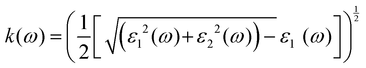
has demonstrated a good refraction value in both the visible and ultraviolet regions of the spectrum. Higher energy states or transitions across the material's band gap are involved in the electronic transitions at higher energies. The refractive index may drop as a result of these transitions in these dichalcogenides. The fluctuation of the WZ2 (Z = S, Se, and Te) compounds’ extinction coefficients k(ω) with energy is shown in Fig. 7(d). For WZ2 (Z = S, Se, and Te), the threshold energies for each compound are 3.0, 2.5, and 2.2 eV, respectively. Above these thresholds, the extinction coefficient steadily increases with energy. The sharp peaks of the k(ω) spectra are observed to occur between 4.5 and 6.0 eV, and the corresponding peak values for WS2, WTe2, and WSe2 are 1.2, 1.6, and 1.8, respectively. Peaks of k(ω) values for the compounds WZ2 (Z = S, Se, and Te) are interpreted physically to represent the materials’ maximum absorption behavior where additional increases in photon energy result in a significant drop in the magnitude of the k(ω) spectra.
. Be aware that there are two significant sharp peaks in each case, which are caused by interband transitions. For WS2, WSe2, and WTe2, respectively, the first set of peaks was precisely present at 5.62, 5.10, and 4.20 eV, while the second set of peaks was at 8.38, 7.89, and 7.20 eV, respectively. Maximum peaks for the real component of the dielectric functions show high light absorption at particular energies. These peaks are a result of the material's electronic states absorbing photons resonantly. These high peaks also depend on the material's band structure and electronic characteristics. The real part of the dielectric function declines and may even turn negative after reaching the highest peaks. This behaviour results from the interaction of the material's band structure and interband transitions. A decrease in the material's capacity to absorb light at these energies is indicated by a drop in the real part of the dielectric function. It is crucial to note that WS2, WSe2, and WTe2 show negative ε1(ω) values in the energy ranges from 9.10 to 9.92 eV, 6.00 to 6.94 eV, and 7.50 to 13.00 eV, respectively. The electronic band structure and the interband transitions in WZ2 (Z = S, Se, and Te) binary chalcogenides control the behavior of the imaginary part ε2(ω) of the dielectric function at higher energies. Fig. 6(b) displays the computed imaginary components ε2(ω) of WZ2 (Z = S, Se, and Te). When energy changes, the plot shows pretty comparable characteristics. As seen, WS2, WSe2, and WTe2 binary chalcogenides, respectively, exhibit sharp peaks at 1.93, 1.72, and 1.50 eV. The most noticeable peaks, however, may be observed at energies of 3.10, 2.75, and 2.23 eV, with maximum values for ε2(ω) of 4.24, 8.50, and 7.68, respectively. The ε2(ω) characteristics exhibit a notable diminishing tendency after these energies, and for energies greater than 10.23 eV, they become insignificant. When the Z atom is switched from Te to Se to S, the rise in the band gap in this direction leads the whole spectra to shift to higher energies. Phase space-filling effects frequently place a cap on the absorption coefficient in materials with a high density of states. This implies that when more electronic states are filled, states are left over for transition. The number of transition-ready states may fill up at higher energies, which would reduce the absorption coefficient. The electron–electron interactions and screening effects are stronger at higher energies. These interactions can alter the material's optical characteristics and have an impact on the dielectric response. At higher energies, the screening effects might lower the absorption coefficient. The computed absorption coefficients of WZ2 (Z = S, Se, and Te) are shown in Fig. 6(c) as a function of energy. It should be noted that the binary chalcogenides WZ2 (Z = S, Se, and Te) exhibit capacity to absorb visible and ultraviolet lights. For WS2, WSe2, and WTe2, the I(ω) maximum values are 85.12, 100.35, and 95.13, respectively. These highest values are precisely located at energies of 11.92, 11.0, and 9.50 eV in the ultraviolet range. The incident photon energy is close to or slightly greater than the material's band gap energy, which causes a peak in the absorption coefficient in the energy range from 5.0 eV to 7.0 eV. The absorption coefficient decreases from 7.5 eV to 10.0 eV in the energy range. This drop occurs because there is less chance that electrons will be driven to the conduction band. After all, the photon energy is now substantially higher than the band gap energy. Fewer photons are being absorbed in this energy range, according to the declining absorption coefficient. The absorption coefficient starts to increase once more above 10.0 eV. The reason for this increase is that the incident photon energy is now greater than the energy of other levels or transitions in the material. As these extra energy levels become accessible, the absorption coefficient increases once more. The plasma oscillations that cause peaks in the energy loss function L(ω) are responsible for these frequencies, which are also known as plasma frequencies. The reason for this is a result of the collective longitudinal reaction of valence electron oscillations to background plasma-frequency atomic cores. As illustrated in Fig. 6(d), energy loss began at 5.0 eV and the energy level changes gradually up to approximately 10.0 eV. The peaks were sharpened at 13.5 eV finally and an isotropic behavior of energy loss functions was noticed. The presence of valence electron excitations can be linked to a decrease in the energy loss function in the 0–8 eV energy range. These excitations include valence band transitions from occupied to unoccupied electronic states. The energy loss function, however, becomes more pronounced at higher energies between 10.0 and 14.0 eV. The WZ2 chalcogenide material's electrical structure and optical characteristics have an impact on how the energy loss function behaves. The precise energy ranges in which these behaviors take place can differ depending on factors like the band gap size, band structure, and material composition. The reflection of electromagnetic radiation from a material is related to the reflectivity dispersion R(ω). The reflectivity R(ω) of WZ2 (Z = S, Se, and Te) compounds against spectral energy is shown in Fig. 7(a). The optical reflectivity R(ω) average of the nonzero components shows that there is no obvious change in the reflectivity spectrum concerning varying material concentrations in the WZ2 compounds. Small fluctuating peaks that are connected to inter-band transitions are accompanied by a striking increase in the reflectivity value. Fig. 7(a) shows an abrupt increase in reflectivity at 5.72 eV, which then gradually decreases as it approaches 8.45 eV. Higher energy range (5.72 to 12 eV) reflectance values for our examined dichalcogenides are similarly good. The materials may show reduced absorption in the energy range where reflectivity increases. This may be caused by the absence of interband transitions or their diminished intensity in that energy range, as well as other absorption mechanisms. Reflectivity increases when incident light is reflected more often than it is absorbed, which reduces absorption. The ability of a substance to conduct light or other electromagnetic radiation is represented by the real part of optical conductivity. The optical conductivity for WZ2 (Z = S, Se, and Te) reaches its peak between 4.0 and 6.0 eV and it falls as the charge concentration increases at point 10.0 eV due to a variety of behaviors. The greater peaks in the real part of the optical conductivity range from 4.0 eV to 9.0 eV indicating considerable absorption or the materials’ capacity to conduct light at these energies. These peaks often signify interband transitions, as electrons move across the band gap from occupied to unoccupied states. The band structure and electrical characteristics of the WZ2 chalcogenide materials determine where these peaks are energetically located. Reduced interband transitions or modifications to the materials’ electronic structure are the reasons for the decline in the real component of the optical conductivity after the energy range of 9.0 eV. The drop in optical conductivity means that these materials have less capacity to conduct or absorb light within that particular energy range. Fig. 7(c) displays the refractive index variation vs. spectral energy for these materials. There is no visible change in the refraction spectra for varying material concentrations in the WZ2 compounds, as shown by the average of non-zero components of the refractive index n(ω). Small fluctuating peaks that are connected to inter-band transitions show a striking increase in the refraction value. Refraction increases abruptly at 3.0 eV and approaches 5.0 eV before decreasing, as shown in Fig. 7(c). At higher energy ranges (6.5 to 10.0 eV), our dichalcogenides under investigation also show good refraction values. It is important to stress that every compound
has demonstrated a good refraction value in both the visible and ultraviolet regions of the spectrum. Higher energy states or transitions across the material's band gap are involved in the electronic transitions at higher energies. The refractive index may drop as a result of these transitions in these dichalcogenides. The fluctuation of the WZ2 (Z = S, Se, and Te) compounds’ extinction coefficients k(ω) with energy is shown in Fig. 7(d). For WZ2 (Z = S, Se, and Te), the threshold energies for each compound are 3.0, 2.5, and 2.2 eV, respectively. Above these thresholds, the extinction coefficient steadily increases with energy. The sharp peaks of the k(ω) spectra are observed to occur between 4.5 and 6.0 eV, and the corresponding peak values for WS2, WTe2, and WSe2 are 1.2, 1.6, and 1.8, respectively. Peaks of k(ω) values for the compounds WZ2 (Z = S, Se, and Te) are interpreted physically to represent the materials’ maximum absorption behavior where additional increases in photon energy result in a significant drop in the magnitude of the k(ω) spectra.
 |
| | Fig. 6 The calculated frequency-dependent (a) real and (b) imaginary components of dielectric functions (c) absorption coefficients and (d) energy loss functions, for WZ2 (Z = S, Se, and Te) materials. | |
 |
| | Fig. 7 The calculated frequency-dependent (a) reflectivity, (b) real part of optical conductivity, (c) refractive index, and (d) extinction coefficient for WZ2 (Z = S, Se, and Te) materials. | |
3.4 Thermoelectric properties
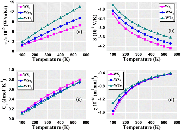
For understanding and evaluating the thermoelectric performance of materials, thermoelectric parameters are vital. These variables determine a material's capacity to turn heat into electricity (the Seebeck effect) or vice versa. Overall, these thermoelectric parameters give materials scientists and engineers crucial knowledge that they may use to create effective thermoelectric materials and devices for a variety of applications, such as waste heat recovery, power generation, and solid-state cooling. The relaxation time plays an important role because it impacts how the relaxation time approximation of the semi-classical Boltzmann transport theory determines the electronic transport coefficient of the TE material. The relaxation time is typically influenced by a variety of scattering phenomena, including magnetic scattering, electron–electron interactions, electron–phonon interactions, defects, and impurity scattering, among others. Choosing a time to rest is so usually difficult. The relaxation time was frequently assumed to be independent of energy and was equal to 8.1 × 10⁻¹⁵ (s) in these thermoelectric property calculations. Fig. 8(a) shows the predicted thermal conductivity of the dichalcogenides WZ2 (Z = S, Se, and Te). The value increases with the chalcogenide's atomic number for temperatures up to 100 K. The values for the WS2, WSe2, and WTe2 compounds at room temperature are 0.04, 0.02, and 0.01 (1015 W m−1 K−1 s−1), respectively. WTe2, WSe2, and WS2 exhibit the maximum thermal conductivity at 550 K. The electronic thermal conductivity values of WS2, WSe2, and WTe2 at 550 K are 8.2, 11.0, and 14.0 (1015 W m−1 K−1 s−1), respectively. Increased thermal transport results from an increase in phonon density at higher temperatures. The thermal conductivity of these dichalcogenides increases as temperature increases because there are more phonons available to transport heat through the lattice. Due to the small number of phonon–phonon interactions at low temperatures in these dichalcogenides, phonon–phonon scattering processes are often less efficient. But when the temperature increases, anharmonic effects become more pronounced, leading to more phonon scattering in these dichalcogenides. By enabling heat transmission through more frequent phonon interactions, this improved scattering can increases thermal conductivity. In the 100 K to 600 K range, the predicted spectra of the Seebeck coefficient for WZ2 (Z = S, Se, and Te) are displayed in Fig. 8(b). The results show that WZ2 (Z = S, Se, and Te) are p-type semiconductors, meaning that there are more holes than electrons throughout the whole temperature range. The S values for WZ2 (Z = S, Se, and Te) typically fall exponentially as the temperature increases. The tendency of Seebeck coefficient values of these dichalcogenides at low temperatures is of the order of Te > Se > S, which is caused by the variation in carrier concentrations. It is the same as that observed by introducing/removing electrons or holes into/from these compounds when Se and Te are used in place of S. When compared to other compounds, WTe2 has the highest value of S at 600 K, which indicates that it contains the fewest holes. The values of S for WZ2 (Z = S, Se, and Te) decrease due to a larger carrier concentration. The system's thermal energy increases together with temperature. As a result, the electronic energy levels become broader, which causes the density of states (DOS) to decline close to the Fermi level. Since the DOS derivative concerning energy determines the Seebeck coefficient, a decline in DOS close to the Fermi level tends to lower the Seebeck coefficient. Furthermore, as temperature increases, the number of phonon scattering events increases in these dichalcogenides, which has an impact on the movement of charge carriers. Phonons, which are lattice vibrations, can scatter charge carriers and obstruct their motion, which lowers the conductivity overall and changes the Seebeck coefficient. The Seebeck coefficient decreases as temperature increases because of the increasing thermal vibrations and scattering mechanisms that cause more interactions between the charge carriers and the phonons.
 |
| | Fig. 8 Calculated (a) thermal conductivity, (b) Seebeck coefficient, (c) specific heat capacity, and (d) susceptibility of the WZ2 (Z = S, Se, and Te) materials. | |
The dominant contribution to the specific heat capacity of tungsten materials is known to come from lattice vibrations, whereas the contribution of free conduction electrons is minimal. Specific heat is an important factor in determining a material's thermal conductivity. High specific heat means that the material can store more heat energy per unit mass, lowering the temperature gradient and influencing thermal conductivity. Fig. 8(c) shows the Cv for WZ2 (Z = S, Se, and Te) structures up to 600 K, where structural stability is still preserved. Our findings show that Cv increases with temperature and becomes closer to the standard Dulong–Petit limit, which is 3NkB, where N is the number of atoms in the unit cell and kB is the Boltzmann constant. The shift of the optical phonon modes with “Z” can be associated with a moderate increase of Cv in the chalcogen group for both phases up to room temperature. At low temperatures, Cv varies more quickly for the high-frequency optical branches than the low-frequency acoustic branches. The behavior of a material's electrons is what causes the electronic component of the specific heat capacity. Low-energy electronic excitations close to the Fermi level often dominate the electronic-specific heat capacity at low temperatures. Thermal stimulation in these dichalcogenides, however, enables more electrons to inhabit higher energy states as the temperature increases. As a result, more electronic states can be used, which increases the electronic-specific heat capacity. The vibrational motion of the atoms in the crystal lattice is linked to the lattice's contribution to the specific heat capacity. Calculating the lattice dynamics and phonon characteristics using DFT can give us information on how the lattice affects the specific heat capacity. The crystal lattice's harmonic vibrations often dominate the lattice contribution at low temperatures. However, when the temperature increases, the importance of anharmonic effects increases, leading to more vibrational modes and a higher lattice-specific heat capacity. WZ2 (Z = S, Se, and Te) exhibit the maximum specific heat capacity at 550 K. The specific heat capacity values of WS2, WSe2, and WTe2 at 550 K are 0.8, 0.75, and 0.76 (Cv) (J mol−1 K−1), respectively. The susceptibility is frequently correlated with the electronic density of states (DOS) and the effective mass of charge carriers in DFT calculations. When the temperature increases, the thermal energy does as well, which causes electrons to occupy higher energy states in these dichalcogenides. The susceptibility is important in thermoelectric materials for numerous reasons: it has a large impact on the electrical and thermal transport properties of thermoelectric materials that is displayed in Fig. 8(d). Understanding the susceptibility aids in determining the influence of magnetic impurities on the electronic structure and transport behavior. It has the potential to improve the thermoelectric efficiency of certain magnetic thermoelectric materials. Low temperatures can cause the DOS at the Fermi level to be relatively low, which reduces the number of electronic states that are available for conduction. Lower susceptibility values may be the outcome of this. The DOS at the Fermi level increases when the temperature increases because thermal energy enables electrons to occupy higher energy states. Due to the increased DOS, there are more charge carriers in these dichalcogenides, which increases vulnerability. The effective mass of charge carriers is another factor that affects susceptibility. Measured by the effective mass, charge carriers’ reactivity to an external electric field can be determined. Due to the scattering of charge carriers by lattice vibrations (phonons), the effective mass of some materials can increase with temperature. The susceptibility is increased due to the higher effective mass. At a higher temperature of 550 K, the maximum susceptibility was around −0.4 × 10⁻¹⁵ m3 mol−1.
4. Conclusions
In conclusion, novel WZ2 (Z = S, Se, and Te) materials’ structural, electrical, optical, and thermoelectric properties were studied employing density functional theory. For these three materials, a semiconducting nature with an indirect band gap was predicted. In the conduction band, band formation ranges from 1.91 to 5.0 eV, while in the valence band region, band formation ranges from 0 to −6.0 eV. These bands are predominantly caused by the W-f and Z-p orbitals. Following is a list of the band gaps in the ascending order: when the atomic number of these chalcogenide atoms increases, the electronic band gap narrows, as the Eg for WS2 > WSe2 > WTe2. The W-f and Z-p states, once more, are also important to the PDOS of the three materials. The well-known inverse relationship between these two parameters predicts that when the chalcogenide “Z” atom is switched from S to Te, the ε1(0) value will move in the opposite direction to the electronic band gap. High light absorption at specific energies can be seen in the real part's maximum peaks of the dielectric function. After reaching its maximum peaks, the dielectric function's real part starts to fall and may even become negative. Interband transitions and the band structure of the materials interact to produce this behavior. The entire hypothetical spectra shift to higher energies when the Z atom is changed from Te to Se to S due to the increase in the band gap in this direction. The screening effects may cause the absorption coefficient to decrease at higher energies. In the energy range, the absorption coefficient falls from 10.0 eV to 7.5 eV. Since the photon energy is now significantly larger than the band gap energy, there is less probability that electrons will be forced into the conduction band. According to the falling absorption coefficient, less photons are being absorbed in this energy range. The energy loss function in the 0–8 eV energy range can be attributed to a reduction in the presence of valence electron excitations. A considerable increase in the reflectivity value is observed in conjunction with small fluctuating peaks associated with inter-band transitions. Greater peaks imply significant absorption or the materials’ ability to conduct light at these energies in the real part of the optical conductivity range from 4.0 eV to 9.0 eV. A dramatic increase in the refraction value can be seen in small fluctuating peaks associated with inter-band transitions. With increasing temperature, there is an increase in phonon density, which leads to increased thermal transport. As temperature increases, more phonons are available to carry heat through the lattice, increasing thermal conductivity. The change in carrier concentrations accounts for the tendency for these compounds’ low-temperature Seebeck coefficient values to be Te > Se > S. Additionally, as the temperature increases, there are more phonon scattering events, which affect charge carriers flow. According to our research, Cv increases with temperature and approaches the typical Dulong–Petit limit. However, when the temperature increases, thermal stimulation enables more electrons to occupy higher energy states. The higher effective mass causes a greater vulnerability.
Author contributions
Banat Gul: software, data curation, and formal analysis. Muhammad Salman Khan: conceptualization, project administration, and writing – original draft, review and editing. Bashir Ahmad: writing – original draft, review and editing. Mostafizur Rahaman: software and data curation. Paride O. Lolika: conceptualization, project administration, and writing – original draft, review and editing. Guenez Wafa: software, formal analysis, and writing – original draft. Hijaz Ahmad: formal analysis and writing – original draft.
Conflicts of interest
The authors declare that they have no known competing financial interests or personal relationships that could have appeared to influence the work reported in this paper.
Acknowledgements
The authors are grateful to Researchers Supporting project number (RSPD2023R674), King Saud University, Riyadh, Saudi Arabia for the financial support.
References
- K. S. Novoselov, D. Jiang, F. Schedin, T. J. Booth, V. V. Khotkevich and S. V. Morozov,
et al.
, Proc. Natl. Acad. Sci. U. S. A., 2005, 102, 10451–10453 CrossRef CAS PubMed.
- R. Tenne and A. Wold, Appl. Phys. Lett., 1985, 47, 707–709 CrossRef CAS.
- R. Khenata, M. Sahnoun, H. Baltache, M. Rérat, A. Reshak and Y. Al-Douri,
et al.
, Phys. Lett. A, 2005, 344, 271–279 CrossRef CAS.
- M. Remskar, A. Mrzel, Z. Skraba, A. Jesih, M. Ceh and J. Demšar,
et al.
, Science, 2001, 292, 479–481 CrossRef CAS PubMed.
- A. Reshak, M. Piasecki, S. Auluck, I. Kityk, R. Khenata and B. Andriyevsky,
et al.
, J. Phys. Chem. B, 2009, 113, 15237–15242 CrossRef CAS PubMed.
- B. Sipos, A. F. Kusmartseva, A. Akrap, H. Berger, L. Forró and E. Tutiš, Nat. Mater., 2008, 7, 960–965 CrossRef CAS PubMed.
- Y. Ding, Y. Wang, J. Ni, L. Shi, S. Shi and W. Tang, Phys. B, 2011, 406, 2254–2260 CrossRef CAS.
- A. Ayari, E. Cobas, O. Ogundadegbe and M. S. Fuhrer, J. Appl. Phys., 2007, 101, 014507 CrossRef.
- K. Rossnagel, L. Kipp, M. Skibowski, C. Solterbeck, T. Strasser and W. Schattke,
et al.
, Phys. Rev. B: Condens. Matter Mater. Phys., 2001, 63, 125104 CrossRef.
- H. Li, B. Wang, J. Chen, H. Jiang, X. Li and J. Liu,
et al.
, Phys. Rev. A: At., Mol., Opt. Phys., 2007, 76, 033405 CrossRef.
- M. S. Khan, T. Alshahrani, B. Haq, S. Azam, G. Khan and H. Alrobei,
et al.
, J. Solid State Chem., 2021, 293, 121778 CrossRef CAS.
- A. M. Gabovich, A. I. Voitenko, J. F. Annett and M. Ausloos, Supercond. Sci. Technol., 2001, 14, R1–R27 CrossRef CAS.
- S. W. Han, H. Kwon, S. K. Kim, S. Ryu, W. S. Yun and D. H. Kim,
et al.
, Phys. Rev. B: Condens. Matter Mater. Phys., 2011, 84, 045409 CrossRef.
- K. K. Kam and B. A. Parkinson, J. Phys. Chem., 1982, 86, 463–467 CrossRef CAS.
- Q. H. Wang, K. Kalantar-Zadeh, A. Kis, J. N. Coleman and M. S. Strano, Nat. Nanotechnol., 2012, 7, 699–712 CrossRef CAS PubMed.
- D. Jariwala, V. K. Sangwan, L. J. Lauhon, T. J. Marks and M. C. Hersam, ACS Nano, 2014, 8, 1102–1120 CrossRef CAS PubMed.
- J. A. Wilson and A. D. Yoffe, Adv. Phys., 1969, 18, 193–335 CrossRef CAS.
- D. L. Greenaway and R. Nitsche, J. Phys. Chem. Solids, 1965, 26, 1445–1458 CrossRef CAS.
- P. A. Lee, G. Said, R. Davis and T. H. Lim, J. Phys. Chem. Solids, 1969, 30, 2719–2729 CrossRef CAS.
- M. G. Bell and W. Y. Liang, Adv. Phys., 1976, 25, 53–86 CrossRef CAS.
- H. P. Hughes and W. Y. Liang, J. Phys. C-Solid State Phys., 1977, 10, 1079–1087 CrossRef CAS.
- S. C. Bayliss and W. Y. Liang, J. Phys. C-Solid State Phys., 1982, 15, 1283–1296 CrossRef CAS.
- P. Novák, R. Imhof and O. Haas, Electrochim. Acta, 1999, 45, 351–367 CrossRef.
- M. Abdulsalam and D. Joubert, Comput. Mater. Sci., 2016, 115, 177–183 CrossRef CAS.
- G. Kalpana, G. Pari, A. Mookerjee and A. K. Bhattacharyya, Int. J. Mod. Phys. B, 1998, 12, 1975–1984 CrossRef CAS.
- A. Fleszar and W. Hanke, Phys. Rev. B: Condens. Matter Mater. Phys., 2000, 62, 2466–2474 CrossRef CAS.
- J. Liu, H. Liu, J. Wang, H. Sheng, G. Tang and J. Zhang,
et al.
, Phys. B, 2019, 568, 18–24 CrossRef CAS.
-
T. R. Tölle, Der Schmerz, 2014, vol. 28, pp. 547–553 Search PubMed.
- P. F. Weck, E. Kim and K. R. Czerwinski, Dalton Trans., 2013, 42, 15288 RSC.
- G. Onida, L. Reining and A. Rubio, Rev. Mod. Phys., 2002, 74, 601–659 CrossRef CAS.
- J. Perdew, K. Burke and M. Ernzerhof, Phys. Rev. Lett., 1996, 77, 3865–3868 CrossRef CAS PubMed.
-
P. Blaha, K. Schwarz, G. K. H. Madsen, D. Hvasnicka and J. Luitz, WIEN2k, an Augmented Plane Wave + Local Orbitals Program for Calculating Crystal Properties, Karlheinz Schwarz, Techn. Universit Wien, Austria, 2001 Search PubMed.
- Z. Wu and R. Cohen, Phys. Rev. B: Condens. Matter Mater. Phys., 2006, 73, 235116 CrossRef.
- M. Moakafi, R. Khenata, A. Bouhemadou, F. Semari, A. Reshak and M. Rabah, Comput. Mater. Sci., 2009, 46, 1051–1057 CrossRef CAS.
- M. Salman Khan, B. Gul, G. Wafa and G. Khan, Phys. Chem. Chem. Phys., 2023, 25, 4035–4046 RSC.
- B. Gul, M. Salman Khan, H. Ahmad and P. Thounthong, J. Solid State Chem., 2023, 318, 123726 CrossRef CAS.
- G. Ding, C. Xie, J. Bai, Z. Cheng, X. Wang and W. Wu, Phys. Rev. B, 2023, 108, L020302 CrossRef CAS.
- Y. Yang, J. Wang, Y. Liu, Y. Cui, G. Ding and X. Wang, Phys. Rev. B, 2023, 107, 024304 CrossRef CAS.
- H. Abu-Farsakh, B. Gul and M. Salman Khan, ACS Omega, 2023, 8, 14742–14751 CrossRef CAS PubMed.
- M. Salman Khan, B. Gul, H. Abu-Farsakh and G. Khan, J. Mater. Chem. C, 2022, 10, 12001 RSC.
- K. Boudiaf, A. Bouhemadou, Y. Al-Douri, R. Khenata, S. Bin-Omran and N. Guechi, J. Alloys Compd., 2018, 759, 32–43 CrossRef CAS.
- D. R. Penn, Phys. Rev., 1962, 128, 2093–2097 CrossRef CAS.
|
| This journal is © The Royal Society of Chemistry 2023 |
Click here to see how this site uses Cookies. View our privacy policy here. 
 Open Access Article
 This Open Access Article is licensed under a Creative Commons Attribution-Non Commercial 3.0 Unported Licence
 b,
Bashir
Ahmad
b,
Mostafizur
Rahaman
c,
Paride O.
Lolika
b,
Bashir
Ahmad
b,
Mostafizur
Rahaman
c,
Paride O.
Lolika


 signifies the bulk energy of the WZ2 system.40,41 To determine the total energies and the isolated free atoms in our work, we estimated the cohesive energies of WS2, WSe2, and WTe2 using DFT calculations. The cohesive energy values for WS2, WSe2, and WTe2 were determined to be 3.56 eV per atom, 3.82 eV per atom, and 4.15 eV per atom, respectively. According to these figures, WS has the strongest bonding of the three materials, while WTe2 has the worst bonding. This conclusion is in line with the trend in the bulk modulus data, which was supported by the finding that WS is the material most resistant to external pressure:40,41
 . Be aware that there are two significant sharp peaks in each case, which are caused by interband transitions. For WS2, WSe2, and WTe2, respectively, the first set of peaks was precisely present at 5.62, 5.10, and 4.20 eV, while the second set of peaks was at 8.38, 7.89, and 7.20 eV, respectively. Maximum peaks for the real component of the dielectric functions show high light absorption at particular energies. These peaks are a result of the material's electronic states absorbing photons resonantly. These high peaks also depend on the material's band structure and electronic characteristics. The real part of the dielectric function declines and may even turn negative after reaching the highest peaks. This behaviour results from the interaction of the material's band structure and interband transitions. A decrease in the material's capacity to absorb light at these energies is indicated by a drop in the real part of the dielectric function. It is crucial to note that WS2, WSe2, and WTe2 show negative ε1(ω) values in the energy ranges from 9.10 to 9.92 eV, 6.00 to 6.94 eV, and 7.50 to 13.00 eV, respectively. The electronic band structure and the interband transitions in WZ2 (Z = S, Se, and Te) binary chalcogenides control the behavior of the imaginary part ε2(ω) of the dielectric function at higher energies. Fig. 6(b) displays the computed imaginary components ε2(ω) of WZ2 (Z = S, Se, and Te). When energy changes, the plot shows pretty comparable characteristics. As seen, WS2, WSe2, and WTe2 binary chalcogenides, respectively, exhibit sharp peaks at 1.93, 1.72, and 1.50 eV. The most noticeable peaks, however, may be observed at energies of 3.10, 2.75, and 2.23 eV, with maximum values for ε2(ω) of 4.24, 8.50, and 7.68, respectively. The ε2(ω) characteristics exhibit a notable diminishing tendency after these energies, and for energies greater than 10.23 eV, they become insignificant. When the Z atom is switched from Te to Se to S, the rise in the band gap in this direction leads the whole spectra to shift to higher energies. Phase space-filling effects frequently place a cap on the absorption coefficient in materials with a high density of states. This implies that when more electronic states are filled, states are left over for transition. The number of transition-ready states may fill up at higher energies, which would reduce the absorption coefficient. The electron–electron interactions and screening effects are stronger at higher energies. These interactions can alter the material's optical characteristics and have an impact on the dielectric response. At higher energies, the screening effects might lower the absorption coefficient. The computed absorption coefficients of WZ2 (Z = S, Se, and Te) are shown in Fig. 6(c) as a function of energy. It should be noted that the binary chalcogenides WZ2 (Z = S, Se, and Te) exhibit capacity to absorb visible and ultraviolet lights. For WS2, WSe2, and WTe2, the I(ω) maximum values are 85.12, 100.35, and 95.13, respectively. These highest values are precisely located at energies of 11.92, 11.0, and 9.50 eV in the ultraviolet range. The incident photon energy is close to or slightly greater than the material's band gap energy, which causes a peak in the absorption coefficient in the energy range from 5.0 eV to 7.0 eV. The absorption coefficient decreases from 7.5 eV to 10.0 eV in the energy range. This drop occurs because there is less chance that electrons will be driven to the conduction band. After all, the photon energy is now substantially higher than the band gap energy. Fewer photons are being absorbed in this energy range, according to the declining absorption coefficient. The absorption coefficient starts to increase once more above 10.0 eV. The reason for this increase is that the incident photon energy is now greater than the energy of other levels or transitions in the material. As these extra energy levels become accessible, the absorption coefficient increases once more. The plasma oscillations that cause peaks in the energy loss function L(ω) are responsible for these frequencies, which are also known as plasma frequencies. The reason for this is a result of the collective longitudinal reaction of valence electron oscillations to background plasma-frequency atomic cores. As illustrated in Fig. 6(d), energy loss began at 5.0 eV and the energy level changes gradually up to approximately 10.0 eV. The peaks were sharpened at 13.5 eV finally and an isotropic behavior of energy loss functions was noticed. The presence of valence electron excitations can be linked to a decrease in the energy loss function in the 0–8 eV energy range. These excitations include valence band transitions from occupied to unoccupied electronic states. The energy loss function, however, becomes more pronounced at higher energies between 10.0 and 14.0 eV. The WZ2 chalcogenide material's electrical structure and optical characteristics have an impact on how the energy loss function behaves. The precise energy ranges in which these behaviors take place can differ depending on factors like the band gap size, band structure, and material composition. The reflection of electromagnetic radiation from a material is related to the reflectivity dispersion R(ω). The reflectivity R(ω) of WZ2 (Z = S, Se, and Te) compounds against spectral energy is shown in Fig. 7(a). The optical reflectivity R(ω) average of the nonzero components shows that there is no obvious change in the reflectivity spectrum concerning varying material concentrations in the WZ2 compounds. Small fluctuating peaks that are connected to inter-band transitions are accompanied by a striking increase in the reflectivity value. Fig. 7(a) shows an abrupt increase in reflectivity at 5.72 eV, which then gradually decreases as it approaches 8.45 eV. Higher energy range (5.72 to 12 eV) reflectance values for our examined dichalcogenides are similarly good. The materials may show reduced absorption in the energy range where reflectivity increases. This may be caused by the absence of interband transitions or their diminished intensity in that energy range, as well as other absorption mechanisms. Reflectivity increases when incident light is reflected more often than it is absorbed, which reduces absorption. The ability of a substance to conduct light or other electromagnetic radiation is represented by the real part of optical conductivity. The optical conductivity for WZ2 (Z = S, Se, and Te) reaches its peak between 4.0 and 6.0 eV and it falls as the charge concentration increases at point 10.0 eV due to a variety of behaviors. The greater peaks in the real part of the optical conductivity range from 4.0 eV to 9.0 eV indicating considerable absorption or the materials’ capacity to conduct light at these energies. These peaks often signify interband transitions, as electrons move across the band gap from occupied to unoccupied states. The band structure and electrical characteristics of the WZ2 chalcogenide materials determine where these peaks are energetically located. Reduced interband transitions or modifications to the materials’ electronic structure are the reasons for the decline in the real component of the optical conductivity after the energy range of 9.0 eV. The drop in optical conductivity means that these materials have less capacity to conduct or absorb light within that particular energy range. Fig. 7(c) displays the refractive index variation vs. spectral energy for these materials. There is no visible change in the refraction spectra for varying material concentrations in the WZ2 compounds, as shown by the average of non-zero components of the refractive index n(ω). Small fluctuating peaks that are connected to inter-band transitions show a striking increase in the refraction value. Refraction increases abruptly at 3.0 eV and approaches 5.0 eV before decreasing, as shown in Fig. 7(c). At higher energy ranges (6.5 to 10.0 eV), our dichalcogenides under investigation also show good refraction values. It is important to stress that every compound
has demonstrated a good refraction value in both the visible and ultraviolet regions of the spectrum. Higher energy states or transitions across the material's band gap are involved in the electronic transitions at higher energies. The refractive index may drop as a result of these transitions in these dichalcogenides. The fluctuation of the WZ2 (Z = S, Se, and Te) compounds’ extinction coefficients k(ω) with energy is shown in Fig. 7(d). For WZ2 (Z = S, Se, and Te), the threshold energies for each compound are 3.0, 2.5, and 2.2 eV, respectively. Above these thresholds, the extinction coefficient steadily increases with energy. The sharp peaks of the k(ω) spectra are observed to occur between 4.5 and 6.0 eV, and the corresponding peak values for WS2, WTe2, and WSe2 are 1.2, 1.6, and 1.8, respectively. Peaks of k(ω) values for the compounds WZ2 (Z = S, Se, and Te) are interpreted physically to represent the materials’ maximum absorption behavior where additional increases in photon energy result in a significant drop in the magnitude of the k(ω) spectra.
. Be aware that there are two significant sharp peaks in each case, which are caused by interband transitions. For WS2, WSe2, and WTe2, respectively, the first set of peaks was precisely present at 5.62, 5.10, and 4.20 eV, while the second set of peaks was at 8.38, 7.89, and 7.20 eV, respectively. Maximum peaks for the real component of the dielectric functions show high light absorption at particular energies. These peaks are a result of the material's electronic states absorbing photons resonantly. These high peaks also depend on the material's band structure and electronic characteristics. The real part of the dielectric function declines and may even turn negative after reaching the highest peaks. This behaviour results from the interaction of the material's band structure and interband transitions. A decrease in the material's capacity to absorb light at these energies is indicated by a drop in the real part of the dielectric function. It is crucial to note that WS2, WSe2, and WTe2 show negative ε1(ω) values in the energy ranges from 9.10 to 9.92 eV, 6.00 to 6.94 eV, and 7.50 to 13.00 eV, respectively. The electronic band structure and the interband transitions in WZ2 (Z = S, Se, and Te) binary chalcogenides control the behavior of the imaginary part ε2(ω) of the dielectric function at higher energies. Fig. 6(b) displays the computed imaginary components ε2(ω) of WZ2 (Z = S, Se, and Te). When energy changes, the plot shows pretty comparable characteristics. As seen, WS2, WSe2, and WTe2 binary chalcogenides, respectively, exhibit sharp peaks at 1.93, 1.72, and 1.50 eV. The most noticeable peaks, however, may be observed at energies of 3.10, 2.75, and 2.23 eV, with maximum values for ε2(ω) of 4.24, 8.50, and 7.68, respectively. The ε2(ω) characteristics exhibit a notable diminishing tendency after these energies, and for energies greater than 10.23 eV, they become insignificant. When the Z atom is switched from Te to Se to S, the rise in the band gap in this direction leads the whole spectra to shift to higher energies. Phase space-filling effects frequently place a cap on the absorption coefficient in materials with a high density of states. This implies that when more electronic states are filled, states are left over for transition. The number of transition-ready states may fill up at higher energies, which would reduce the absorption coefficient. The electron–electron interactions and screening effects are stronger at higher energies. These interactions can alter the material's optical characteristics and have an impact on the dielectric response. At higher energies, the screening effects might lower the absorption coefficient. The computed absorption coefficients of WZ2 (Z = S, Se, and Te) are shown in Fig. 6(c) as a function of energy. It should be noted that the binary chalcogenides WZ2 (Z = S, Se, and Te) exhibit capacity to absorb visible and ultraviolet lights. For WS2, WSe2, and WTe2, the I(ω) maximum values are 85.12, 100.35, and 95.13, respectively. These highest values are precisely located at energies of 11.92, 11.0, and 9.50 eV in the ultraviolet range. The incident photon energy is close to or slightly greater than the material's band gap energy, which causes a peak in the absorption coefficient in the energy range from 5.0 eV to 7.0 eV. The absorption coefficient decreases from 7.5 eV to 10.0 eV in the energy range. This drop occurs because there is less chance that electrons will be driven to the conduction band. After all, the photon energy is now substantially higher than the band gap energy. Fewer photons are being absorbed in this energy range, according to the declining absorption coefficient. The absorption coefficient starts to increase once more above 10.0 eV. The reason for this increase is that the incident photon energy is now greater than the energy of other levels or transitions in the material. As these extra energy levels become accessible, the absorption coefficient increases once more. The plasma oscillations that cause peaks in the energy loss function L(ω) are responsible for these frequencies, which are also known as plasma frequencies. The reason for this is a result of the collective longitudinal reaction of valence electron oscillations to background plasma-frequency atomic cores. As illustrated in Fig. 6(d), energy loss began at 5.0 eV and the energy level changes gradually up to approximately 10.0 eV. The peaks were sharpened at 13.5 eV finally and an isotropic behavior of energy loss functions was noticed. The presence of valence electron excitations can be linked to a decrease in the energy loss function in the 0–8 eV energy range. These excitations include valence band transitions from occupied to unoccupied electronic states. The energy loss function, however, becomes more pronounced at higher energies between 10.0 and 14.0 eV. The WZ2 chalcogenide material's electrical structure and optical characteristics have an impact on how the energy loss function behaves. The precise energy ranges in which these behaviors take place can differ depending on factors like the band gap size, band structure, and material composition. The reflection of electromagnetic radiation from a material is related to the reflectivity dispersion R(ω). The reflectivity R(ω) of WZ2 (Z = S, Se, and Te) compounds against spectral energy is shown in Fig. 7(a). The optical reflectivity R(ω) average of the nonzero components shows that there is no obvious change in the reflectivity spectrum concerning varying material concentrations in the WZ2 compounds. Small fluctuating peaks that are connected to inter-band transitions are accompanied by a striking increase in the reflectivity value. Fig. 7(a) shows an abrupt increase in reflectivity at 5.72 eV, which then gradually decreases as it approaches 8.45 eV. Higher energy range (5.72 to 12 eV) reflectance values for our examined dichalcogenides are similarly good. The materials may show reduced absorption in the energy range where reflectivity increases. This may be caused by the absence of interband transitions or their diminished intensity in that energy range, as well as other absorption mechanisms. Reflectivity increases when incident light is reflected more often than it is absorbed, which reduces absorption. The ability of a substance to conduct light or other electromagnetic radiation is represented by the real part of optical conductivity. The optical conductivity for WZ2 (Z = S, Se, and Te) reaches its peak between 4.0 and 6.0 eV and it falls as the charge concentration increases at point 10.0 eV due to a variety of behaviors. The greater peaks in the real part of the optical conductivity range from 4.0 eV to 9.0 eV indicating considerable absorption or the materials’ capacity to conduct light at these energies. These peaks often signify interband transitions, as electrons move across the band gap from occupied to unoccupied states. The band structure and electrical characteristics of the WZ2 chalcogenide materials determine where these peaks are energetically located. Reduced interband transitions or modifications to the materials’ electronic structure are the reasons for the decline in the real component of the optical conductivity after the energy range of 9.0 eV. The drop in optical conductivity means that these materials have less capacity to conduct or absorb light within that particular energy range. Fig. 7(c) displays the refractive index variation vs. spectral energy for these materials. There is no visible change in the refraction spectra for varying material concentrations in the WZ2 compounds, as shown by the average of non-zero components of the refractive index n(ω). Small fluctuating peaks that are connected to inter-band transitions show a striking increase in the refraction value. Refraction increases abruptly at 3.0 eV and approaches 5.0 eV before decreasing, as shown in Fig. 7(c). At higher energy ranges (6.5 to 10.0 eV), our dichalcogenides under investigation also show good refraction values. It is important to stress that every compound
has demonstrated a good refraction value in both the visible and ultraviolet regions of the spectrum. Higher energy states or transitions across the material's band gap are involved in the electronic transitions at higher energies. The refractive index may drop as a result of these transitions in these dichalcogenides. The fluctuation of the WZ2 (Z = S, Se, and Te) compounds’ extinction coefficients k(ω) with energy is shown in Fig. 7(d). For WZ2 (Z = S, Se, and Te), the threshold energies for each compound are 3.0, 2.5, and 2.2 eV, respectively. Above these thresholds, the extinction coefficient steadily increases with energy. The sharp peaks of the k(ω) spectra are observed to occur between 4.5 and 6.0 eV, and the corresponding peak values for WS2, WTe2, and WSe2 are 1.2, 1.6, and 1.8, respectively. Peaks of k(ω) values for the compounds WZ2 (Z = S, Se, and Te) are interpreted physically to represent the materials’ maximum absorption behavior where additional increases in photon energy result in a significant drop in the magnitude of the k(ω) spectra.