
 Open Access Article
 This Open Access Article is licensed under a Creative Commons Attribution-Non Commercial 3.0 Unported Licence
Cold- and hot-casting to regulate the morphology and charge carrier dynamics of CsBi3I10 towards efficient and stable thin-film solar cells†
Xuejiao
Wu
a,
Peiyao
Dong
a,
Li
Yang
*ab and
Jinbao
Zhang
 *ab
*ab
aCollege of Materials, Fujian Key Laboratory of Advanced Materials, Xiamen Key Laboratory of Electronic Ceramic Materials and Devices, Xiamen University, Xiamen, 361005, China. E-mail: jinbao.zhang@xmu.edu.cn
bShenzhen Research Institute of Xiamen University, Shenzhen, 518000, China
First published on 5th September 2023
Abstract
Inorganic semiconductor CsBi3I10 (CBI) emerges as one of the most promising candidates for lead-free perovskite solar cells (PSCs) due to its low toxicity, high visible light absorption and excellent humidity tolerance. However, poor film morphology and high crystal defects limit its practical application in photovoltaics. Herein, hot-casting and cold-casting technologies are proposed respectively in the fabrication process of CBI to regulate the film quality and photoelectric properties. Significant differences appear in the crystallization process and film morphology of CBI layers, resulting in distinct device performance. In contrast to the CBI film with low density and high thickness formed via the hot-casting technology, the cold-casting accelerates the crystallization rate of CBI, achieving a dense and smooth film with moderate thickness. Consequently, cold-casting improves the crystallinity, smoothness, conductivity and hydrophobicity of the CBI films, all of which contribute to the promotion of charge separation at the interface and the inhibition of non-radiative recombination in the PSCs. The resulting devices exhibit a 2-fold increase in the power conversion efficiency and enhanced environmental stability compared to the devices with pristine CBI. This work provides new insights into the crystallization mechanism of bismuth-based films and proposes another approach for regulating the morphology of perovskite films.
Introduction
Hybrid inorganic–organic perovskite solar cells (PSCs) have attracted much attention due to their excellent optoelectronic performance along with a simple fabrication process and low material cost.1,2 To date, the power conversion efficiency (PCE) achieved of typical lead-based PSCs is over 25%, which is comparable to that of silicon solar cells.3 However, environmental contamination by toxic Pb elements has become one of the concerns in the industrialization process of lead-based devices.4,5 Therefore, researchers have focused their attention on seeking for nontoxic metal halide perovskite alternatives to solve this problem. Bismuth (Bi)-based perovskite analogue CsBi3I10 (CBI) exhibits a small bandgap (1.77 eV), high visible light absorption, and excellent humidity tolerance as well as low toxicity, making it become one of the most promising candidates for Pb-free perovskite solar cells.6,7 Some early attempts such as solvent engineering,8 additive strategies,9 element doping10 and charge transport layer optimization11,12 have been adopted to further explore and improve the photoelectric properties of CsBi3I10 film solar cells. However, CsBi3I10 is still not dazzling due to its lower PCEs compared to other bismuth-based materials such as Cs2AgBiBr6,13,14 Cs3Bi2I94,15 and AgBiS2.16One of the crucial factors limiting the performance of CBI-based devices is the poor film morphology with many pinholes and high roughness, which are often caused by the uncontrollable crystallization process of CBI. These issues result in large current leakage and poor charge extraction efficiency in the solar cell devices.17–20 Besides, CBI-based devices exhibited significantly lower open-circuit voltage (Voc) than the other bismuth-based PSCs due to internal defects and shorter carrier lifetime in the CBI layers.21,22 In order to improve the morphology of CBI films, Pandiyarajan and coworkers optimized the solvent composition and developed an anti-solvent dripping technology to gain dense and smooth CBI films, achieving the maximum PCE of 0.63%.8 Liang et al. annealed CBI in the mixed solvent atmosphere (DMF![[thin space (1/6-em)]](https://www.rsc.org/images/entities/char_2009.gif) :DMSO = 4:1), achieving a better film morphology and higher PCEs.23 Recently, our group introduced Pb(SCN)2 in the CBI precursor solution to accelerate the crystallization process, leading to the formation of CBI films with high density and devices with superior performance.9 All of these studies indicate that tailoring the morphology and crystallization process of CBI films is crucial to optimize the photovoltaic performance of bismuth-based PSCs.
:DMSO = 4:1), achieving a better film morphology and higher PCEs.23 Recently, our group introduced Pb(SCN)2 in the CBI precursor solution to accelerate the crystallization process, leading to the formation of CBI films with high density and devices with superior performance.9 All of these studies indicate that tailoring the morphology and crystallization process of CBI films is crucial to optimize the photovoltaic performance of bismuth-based PSCs.
Generally, a favorable crystallization process in the film should include fast nucleation and slow growth to increase the film density and grain size simultaneously.24,25 However, due to the intrinsic properties of the CBI precursor solution, it is hard to achieve an ideal nucleation and growth rate during the crystallization process in the film, resulting in holes and small grain sizes inside the films.19 Therefore, it is challenging to optimize the crystallization rate of CBI to improve the quality of films. Hot-casting is widely used in the fabrication of lead-based perovskite solar cells, which was suggested to increase the grain size and regulate the crystallization rate of perovskites.25–28 By adopting the hot-casting method, millimeter-scale lead-based perovskite gains have been fabricated and applied to solar cells.26 Similarly, low temperature assisted crystallization technology has also been used in the preparation of perovskite films. It has been reported that immersing the as-cast precursor film in liquid nitrogen before annealing could decouple the nucleation and crystallization processes, resulting in highly uniform nucleation sites and dense films.29 Inspired by this, we applied hot-casting and cold-casting technology to fabricate CBI films and revealed their different effects on controlling the film morphology and crystallization process, leading to a large variation in the photovoltaic performance of devices. Surprisingly, cold-casting accelerated the crystallization rate of CBI, promoting the growth of dense and smooth films with moderate thickness and resulting in the improvement of crystallinity and electrical conductivity in the film. As a consequence, the charge separation and extraction at the interface was greatly improved and the non-radiative recombination in the PSCs was highly inhibited. The as-prepared devices showed an increased PCE from 0.34% (pristine CBI) to 0.63%. Meanwhile, both films and devices fabricated by the cold-casting technology exhibited superior water resistance and stability.
Results and discussion
Properties of CsBi3I10 films
We first investigated the influence of different substrate temperatures on the morphology and properties of films. For hot-casting, the SnO2 substrate was preheated on a hot table at 85 °C for 5 min and then quickly transferred to a spin coater for the deposition of CBI precursor solution. During the cold-casting fabrication process, the SnO2 substrate was precooled on a cold table (−5 °C) for 5 min. Fig. 1 shows the processing scheme for CBI films fabricated by different methods. Notably, the CBI film without any treatment is uneven with some white macroscopic stripes on the surface. The CBI film fabricated by hot-casting (Hot-CBI) appears scattered and rough, which is quite different from the film (black and smooth) prepared by the cold-casting (Cold-CBI). However, the same pretreatment (preheat and precool) for the precursor solution did not cause similar dramatic changes in substrate treatment in film morphology and device performance, as shown in Fig. S1 (ESI†). This suggests that the substrate temperature plays a crucial role in the crystallization process of perovskites, which highly affects the volatilization of solvent and the conduction of heat energy in the film.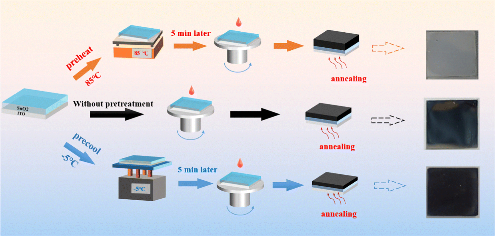 | ||
| Fig. 1 The processing scheme for CBI films fabricated via cold-casting, hot-casting and standard methods. | ||
To further reveal the morphology of CBI layers prepared by different film-forming methods, scanning electron microscopy (SEM) was performed. As shown in Fig. 2(a), many small particles and sparse large grains are distributed on the surface of pristine CBI film, giving low density due to the presence of many small pinholes in the film. Compared with the pristine CBI, Cold-CBI shows more uniform grains and greatly reduced pinholes, making the film more compact. For the Hot-CBI, there are still many large holes through the whole film although the CBI grain size is obviously increased, which could lead to direct contact between the electron transport layer and the hole transport layer and also increase the risk of carrier non-radiative recombination.
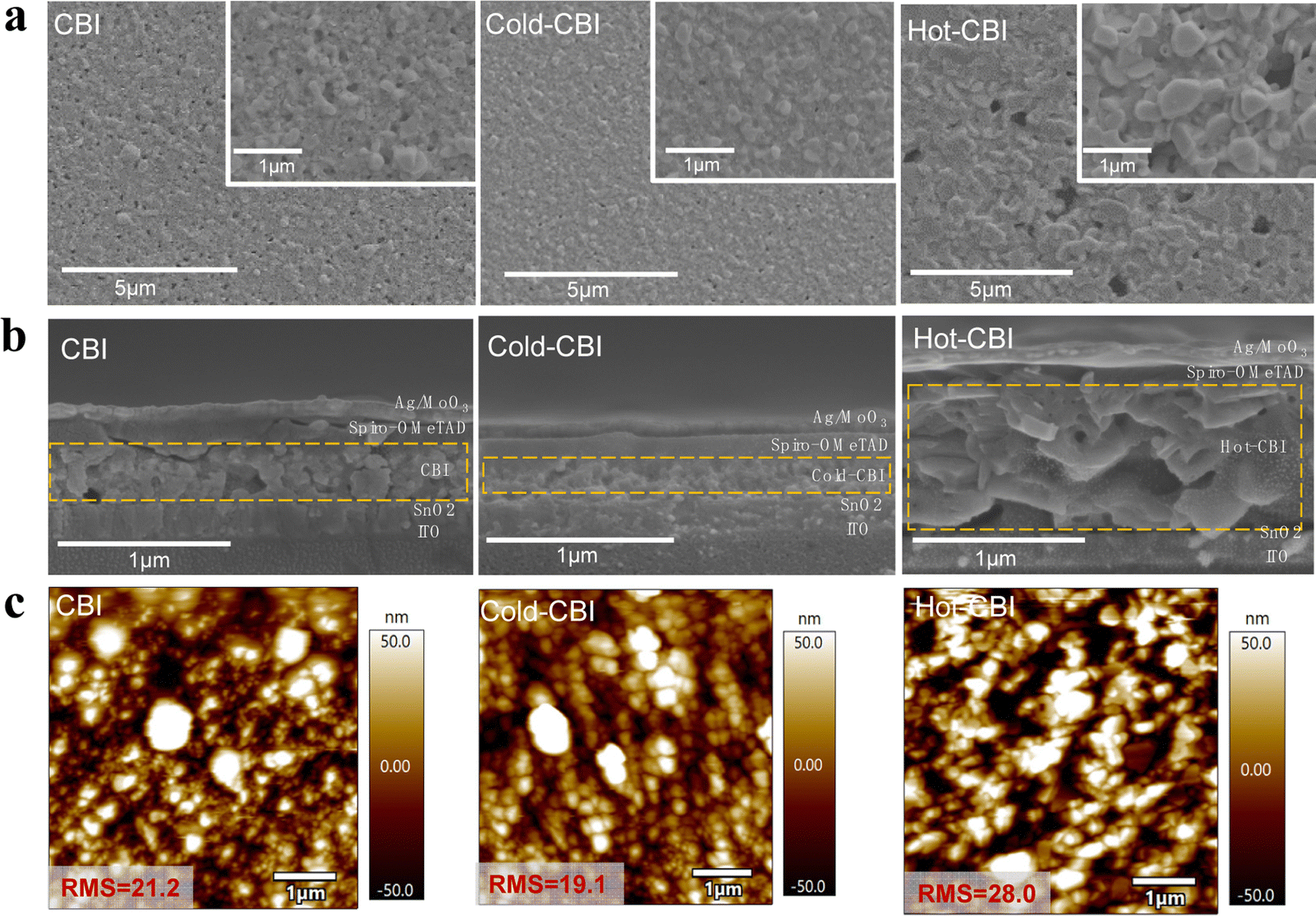 | ||
| Fig. 2 (a) Top-view SEM images of CBI films fabricated by normal, cold-casting and hot-casting technologies. (b) Cross-sectional SEM images of different devices based on CBI, Cold-CBI and Hot-CBI films. (c) AFM images of different CBI films. | ||
The cross-section SEM of the PSCs based on different CBI films are displayed in Fig. 2(b). It can be seen that there are some pinholes in the pristine CBI and small cracks between the CBI layer and spiro-OMeTAD, all of which are detrimental to the photovoltaic performance of the devices. In contrast, the Cold-CBI film is much denser and showed a reduced thickness compared with untreated CBI. Surprisingly, the Hot-CBI film exhibited much higher thickness compared with other samples. The perovskite thickness increase on hot substrates is mainly due to a higher density of heterogeneous nuclei in the film,25,30 which could cause excessive stack growth of crystals. Besides, the greatly promoted grain size further enables a large thickness of the film. In contrast, the lower thickness of the Cold-CBI film may result from its smaller grain size compared with other samples, which is caused by a faster growth process (more details are provided in Fig. 4c). This porous structure and high thickness of Hot-CBI could be fatal for the separation and extraction of the carriers at the interface, resulting in serious non-radiative recombination.30,31 Atomic force microscopy (AFM) was then performed to verify the difference in the roughness of various CBI films. From Fig. 2(c), the Hot-CBI film showed the highest roughness (RMS = 28.0), indicating the most uneven surface morphology. The Cold-CBI film exhibited the lowest roughness (RMS = 19.1), which could enable good contact between the CBI active layer and the hole transport layer.
X-ray diffraction (XRD) was used to investigate the quality of CBI films formed on the substrates with various temperatures. As shown in Fig. 3(a), the diffraction peaks of all the films are similar to those reported in previous literature, which proves the successful formation of CBI crytals.32 Specifically, the intensity of diffraction peaks for Cold-CBI is stronger than that of the pristine CBI, indicating better crystallinity of the film prepared by cold-casting. Meanwhile, the diffraction peak of Hot-CBI film shows extremely strong intensity, which could be due to the large-grained crystals as shown in Fig. 2(a). The Ultraviolet-visible (UV-vis) absorption curves of different films are shown in Fig. 3(b). The absorbance of the Cold-CBI is slightly smaller than that of the pristine CBI film probably due to its smaller thickness. Similarly, the Hot-CBI film shows greatly enhanced absorption at the range of 500–700 nm due to its obviously promoted thickness. Meanwhile, the peak (wavelength <500 nm) was regarded as the exciton absorption peak of CsBi3I10. This is caused by the direct transition of electrons from the valence band to the exciton level below the conduction band after absorbing the photon.33,34 The exciton absorption peak of Hot-CBI significantly become wider compared to those of other samples, which may be due to the deterioration of the quality of Hot-CBI films. This is similar to the report that the absence of DMSO in the precursor solution led to the disappearance of the peak, which was caused by the poor film quality compared to those with DMSO.8 To reveal the electrical properties of films, the conductivity of different CBI layers was evaluated by measuring the current–voltage (I–V) curves of the devices (ITO/CBI). As shown in Fig. 3(c), the pristine CBI and Hot-CBI film exhibited lower conductivity compared to Cold-CBI, which is due to their poor film morphology with low density. Those non-negligible holes as defects inside the film could become recombination centers, causing serious non-radiative recombination of carriers. Therefore, the loss of carriers is aggravated and the carrier migration is hindered in the films, both which of lead to the lowering of the conductivity of the material.35,36 The high conductivity of Cold-CBI films favors the charge transportation, and improves the charge collection efficiency in the devices.37
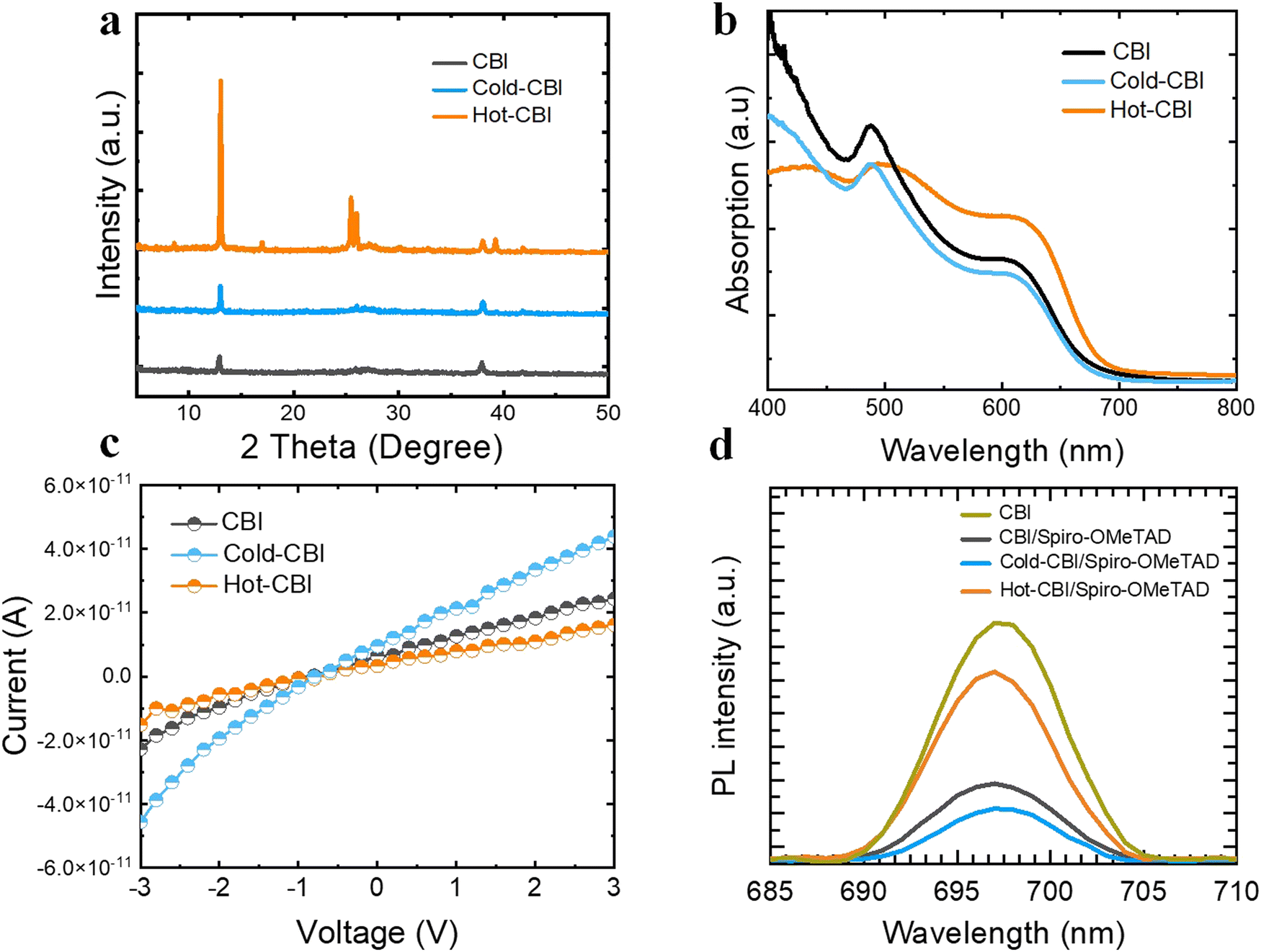 | ||
| Fig. 3 (a) XRD patterns and (b) UV-vis absorption spectra of CBI, Cold-CBI and Hot-CBI films. (c) I–V curves of different CBI films measured on a four-point probe station. (d) PL spectra for CBI, CBI/spiro-OMeTAD, Cold-CBI/spiro-OMeTAD and Hot-CBI/spiro-OMeTAD. | ||
As mentioned above, the hole transport layer presents various coverage degrees because of the different thickness and surface roughness of CBI films. As shown in Fig. S2 (ESI†), the spiro-OMeTAD covering the Cold-CBI film appears purple in color, much darker than the pristine CBI. However, the spiro-OMeTAD film on the Cold-CBI film looks blue and yellow, which is closer to the color of the annealed CBI. To further explore the separation and extraction of charges at the interface between the CBI films and spiro-OMeTAD, steady-state photoluminescence (PL) was used to measure the luminescence intensity of multilayer films with different structures. As shown in Fig. 3(d), the CBI film without the hole transport layer shows the highest PL strength because no hole transport materials are accepting the photogenerated carriers. As for the film with Hot-CBI/spiro-OMeTAD structure, high PL strength was also obtained most likely due to the large holes, high surface roughness and excessive thickness of the CBI film, which makes the hole extraction at the interface extremely difficult. However, the film corresponding to the Cold-CBI/spiro-OMeTAD structure shows the lowest PL intensity. The improved charge separation and extraction at the interfaces demonstrates that cold-casting is a highly effective approach compared with other methods used in this work.38 Besides, we investigated the surface chemistry of three kinds of films by X-ray photoelectron spectroscopy (XPS). As shown in the Fig. S3 (ESI†), we marked the location of the metal bismuth peak with “*”. The XPS curves of the three films show negligible differences, which may result from their identical precursor composition. This indicates that both hot-casting and cold-casting technologies do not increase the content of metallic bismuth inside the films and therefore impact the carrier non-radiative recombination kinetics in the devices. However, the presence of metallic bismuth in all fabricated CBI film is still a factor limiting the Voc and performance of device.33
The microstructure and optoelectronic properties of perovskites are usually determined by the nucleation and growth of films. In order to investigate the effect of preheating and precooling substrates on the crystallization behavior of CBI films, a comparative experiment was conducted. Three kinds of unannealed films were exposed to ambient air for a period of time to allow crystals to grow. Fig. 4(a) shows the color change of different precursor films over time. As displayed in the photographs, the Cold-CBI film turned black firstly after only 5 h of placement. Nevertheless, the pristine CBI film did not turn black until 12.5 h later. Notably, the Hot-CBI film still remained orange during the same time period. All of these results suggest that the cold-casting could accelerate the growth of CBI crystals whereas hot-casting has the opposite effect. To further verify this conclusion, the XRD test was employed to detect the structural evolution of CBI films in the crystallization process. As shown in Fig. 4(b), the characteristic peak (2 Theta = 13.2 degree) of the CBI film gradually changes in intensity as time increases. For the pristine CBI film, this characteristic peak did not appear until 17.5 h later. The peak for the Cold-CBI film appeared obviously after 5h. In contrast, the Hot-CBI characteristic peak still did not grow significantly after 17.5 h. The evolution of XRD peaks is highly consistent with the color change of the films, which indicates that the lower substrate temperature is beneficial to enhancing the crystal growth rate of CBI films. In most instances, the growth rate of crystals is positively related to the diffusion coefficient of solution and inversely proportional to the viscosity.39 Therefore, the slower growth rate of Hot-CBI may be due to the increase in the viscosity of solution in the precursor films, which is caused by excessive removal of solvents on heated substrate and an increase in solution concentration. This makes the solute diffusion to the crystal surface more difficult and slow, resulting in a slower growth process of perovskite. In contrast, the residual Cold-CBI precursor solution has lower viscosity due to the precipitation of more nuclei and normal removal of solvent, leading to a faster growth process, as shown in Fig. 4(c).
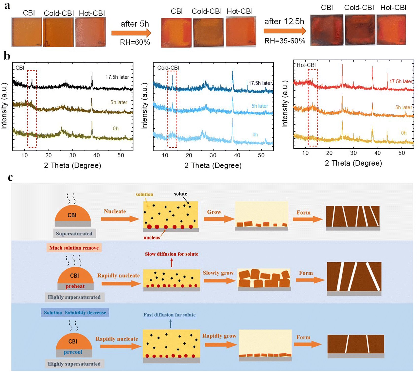 | ||
| Fig. 4 (a) The photographs of unannealed CBI, Cold-CBI and Hot-CBI films changing over time in humid air. (b) XRD patterns of different unannealed CBI films over time. (c) Schematic diagram of the possible crystallization mechanism of different CBI films. | ||
The crystallization process of CBI films includes two stages: nucleation and growth. Unlike the crystal growth completed during annealing process, the nucleation of film occurs in the spin coating process is usually accompanied with the instantaneous supersaturation of solution.40 As discussed above, we reasonably speculated the nucleation processes of different CBI films and proposed a rational crystallization mechanism. As shown in Fig. 4(c), the pristine CBI film prepared at moderate conditions contains small grains, many holes and medium thickness, which is owing to its non-ideal nucleation and growth rate. For the Hot-CBI film, abundant crystal nuclei were rapidly formed on the preheated substrate (85 °C) because the solvent evaporates quickly at a high temperature and reaches its supersaturation level in a shorter time, as previously reported.25,27,40,41 Then those nuclei grew up at a slow rate to form large grains (as shown in Fig. 4(a) and (b)). Due to the limited space of the substrate and an obvious increase in nucleus number, partial grain stacking up for further growth occurred and a film with coarse grains, huge holes and high thickness was formed eventually. When decreasing the temperature down to −5 °C, the solvent evaporation rate does not change significantly due to the high boiling point of solvent and small difference between the room temperature (about 18 °C) and the substrate temperature. But the solubility of the CBI components decreased rapidly (Fig. S4, ESI†), which could make the solution reach the supersaturation level faster. Therefore, more nuclei were also generated at a fast rate. A quick growing process was then followed, which makes grains grow more evenly, resulting in a Cold-CBI film with high density, fine grains and thin thickness.
Device performance
In order to evaluate the photovoltaic performance of different CBI films, n–i–p PSCs with a planar structure of ITO/SnO2/CsBi3I10/spiro-OMeTAD/MoO3/Ag were fabricated, as shown in Fig. 5(a). Fig. 5(b) shows the current–voltage (J–V) curves of solar cells, and the parameters of corresponding devices are displayed in Table 1. All kinds of devices exhibit varying degrees of hysteresis, as shown in Fig. S5 and Table S1 (ESI†). The distribution of PCE and other parameters of three kinds of devices are shown in Fig. 5(c) and Fig. S6 (ESI†). The device based on pristine CBI exhibits a champion PCE of 0.34%, a Voc of 0.44 V, a short-circuit current (Jsc) of 2.26 mA cm−2, and a fill factor (FF) of 33.50%. The Hot-CBI device displays the worst performance with a PCE of 0.14% due to significantly reduced Voc and Jsc. The Cold-CBI PSC exhibits the most outstanding photoelectric performance, with a highest PCE of 0.63%, a Voc of 0.47 V, a Jsc of 3.64 mA cm−2 and a FF of 36.83%. The promotion of Voc and Jsc is most likely due to the improvement of film morphology and carrier extraction efficiency. However, the FF is quite low for all devices, which may be due to the unregulated structure of devices and the charge transport layer in this work.42 Electrochemical impedance (EIS) measurements were performed under dark conditions to clarify the interface charge transport characteristics of CBI-based devices, as shown in Fig. 5(d). According to the previous literature, Rs, Rct and Rrec represents the series resistance, the charge transfer resistance, the recombination impedance of the carriers, respectively. CPE is on behalf of the constant phase element. The first arc appearing in the high-frequency region represents the charge transfer resistance of whole device.43 As displayed in the figure, the Cold-CBI device shows the smallest Rct, suggesting the decrease of charge transfer resistance at the interface and an increase of the driving force for charge separation in devices. In contrast, the device based on Hot-CBI film gives the largest Rct, possibly because the large holes and high thickness of the active layer inhibit the separation and extraction of charge carriers.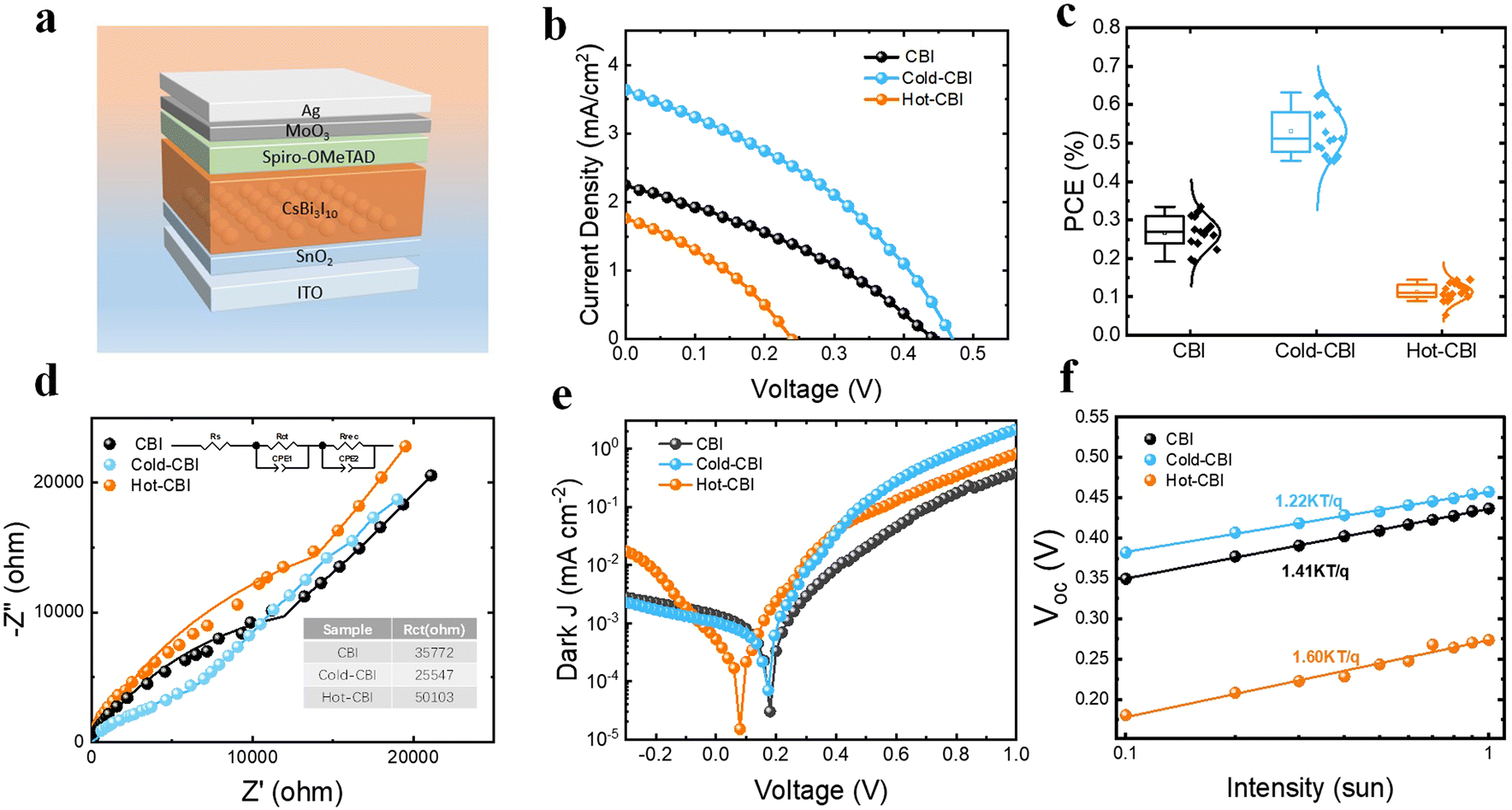 | ||
| Fig. 5 (a) CBI-based planar device configuration with ITO/SnO2/CsBi3I10/spiro-OMeTAD/MoO3/Ag. (b) J–V curves of the champion devices based on CBI, Cold-CBI and Hot-CBI films. (c) Distribution of PCEs of three types of PSCs fabricated via different methods. (d) Nyquist plots of PSCs measured at a potential of 0.1 V and frequency range from 1000 to 106 Hz. (e) Dark I–V curves of devices based on different perovskite films. (f) Voc dependence as a function of light intensity for different PSCs. | ||
| Samples | V oc (V) | J sc (mA cm−2) | FF (%) | PCE (%) |
|---|---|---|---|---|
| CBI | 0.44 | 2.26 | 33.50 | 0.34 |
| Cold-CBI | 0.47 | 3.64 | 36.83 | 0.63 |
| Hot-CBI | 0.24 | 1.76 | 34.28 | 0.14 |
Dark J–V curves of devices based on different CBI films were also measured, as shown in Fig. 5(e). The curve of the Cold-CBI device shows the maximum slope in the range of 0–1 V among all samples, which means that it has the minimum series resistance. This may be caused by the promotion in the conductivity of Cold-CBI films, resulting in an enhancement of FF.44,45 The curve corresponding to the Hot-CBI device also shows significantly increased slope in the range of −0.3–0 V, confirming its smallest shunt resistance, which may come from increased pinholes and nonuniformities in the Hot-CBI layer, leading to serious loss of Voc in the devices.46Fig. 5(f) shows the Voc dependence of different devices on light intensity. There is a linear relationship between Voc and logarithm of light intensity for all samples, whose slope is nkT/q. As shown, the calculated n value of the Cold-CBI device is 1.22, which is lower than that of the pristine CBI device (n = 1.41) and the Hot-CBI device (n = 1.60). This indicates the cold-casting could effectively inhibit the carrier non-radiative recombination inside the device and suppress the loss of carriers at the interface. The external quantum efficiency (EQE) spectra of three types of CsBi3I10 PSCs are shown in Fig. S7 (ESI†). The Jsc calculated by EQE spectrum (Cold-CBI: 3.38 mA cm−2, CBI: 2.06 mA cm−2, Hot-CBI: 1.62 mA cm−2) is close to the measured valued from the J–V curve. The Cold-CBI based device shows significantly enhanced EQE in the wavelength range from 300 nm to 700 nm compared to other samples. This is due to the enhanced conductivity of films, inhibition of interfacial recombination and improved charge separation in the device, resulting in a better carrier extraction efficiency of PSCs.
Stability test
Stability is one of the most significant indexes to verify the reliability of the absorption layer. The humidity tolerance is mainly determined by its hydrophobicity. Herein, the contact angles of different CBI films were tested. As shown in Fig. 6(a), the contact angle of the pristine CBI film is 78.0°, which is smaller than that of the Cold-CBI film (82.1°). This indicates the superior hydrophobicity of the Cold-CBI film, which could improve the humidity stability of the devices. A higher contact angle could be attributed to the denser morphology of the Cold-CBI film as previously discussed, which makes it difficult for moisture to spread out through the film. Further study shows that when both CBI and Cold-CBI films were exposed to humid air (relatively humidity (RH) = 65%, 18 °C) for a period of time, the characteristic diffraction intensity of the pristine CBI film decreased significantly after 148 h (Fig. 6(b)). In contrast, the peak intensity of the Cold-CBI film keeps almost unchanged, suggesting the film has a much better humidity stability.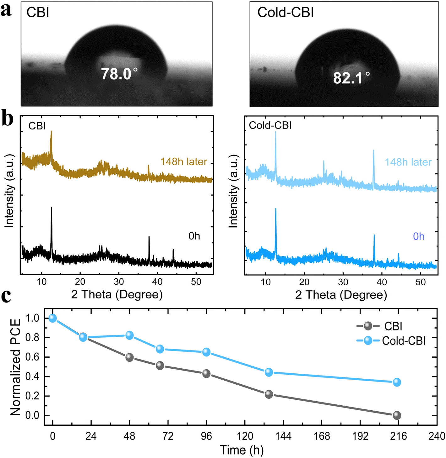 | ||
| Fig. 6 (a) Contact angles of water on the CBI and Cold-CBI film. (b) XRD patterns of both CBI and Cold-CBI films changed over time when stored in ambient air (RH = 65%, 18 °C). (c) Normalized photovoltaic parameters of unencapsulated PSCs in air with a humidity of 30%. | ||
Meanwhile, the environmental stability of unencapsulated devices was tested under relatively humid conditions (RH = 30%, 18 °C). As can be seen from Fig. (6c), the PCE of pristine CBI device declines rapidly and no reliable I–V curves could be detected after 216 h due to the complete degradation occurring in the device. However, the device based on Cold-CBI film retains 37% of initial efficiency after 216 h, indicating a longer life-time of the devices fabricated using the cold-casting technology. The better stability of Cold-CBI based devices may result from both films and hole transport layers. Cold-CBI films show better stability, which could improve serious non-radiation recombination in the device come from aging perovskite. Besides, the tBp we used in hole transport layer has been reported could dissolves bismuth-based perovskite, which easily leads to rapid degradation of devices. The tBp may penetrate with more difficulty into the Cold-CBI film with better morphology and higher density, leading to a slower degradation of PSCs.47
Conclusions
Both cold-casting and hot-casting technologies have been applied to regulate the crystallization process of CsBi3I10 films in this work. The morphology and crystallization mechanism of CBI based on different substrates with various temperatures were systematically investigated. By using hot-casting technology, the growth rate of CBI crystals was decelerated and a film with large holes, high roughness and ultra-thick thickness was obtained. In contrast, cold-casting improved the density, flatness and electrical conductivity of the CBI film by accelerating the crystallization rate, which effectively promoted the charge separation and extraction at the interface between CBI and the hole transport layer. As a consequence, the Cold-CBI based PSCs exhibits an increased PCE from 0.34% to 0.63%. Meanwhile, a higher hydrophobicity has been achieved for the film prepared by using the cold-casting method. The unencapsulated device based on Cold-CBI also displays preferable water stability, retaining approximately 40% of the initial PCE after 216 hours in air. This work provides new insights into the crystallization kinetics of bismuth-based perovskites and offers another way to regulate the CBI film quality, which could be applicable to other perovskite materials.Conflicts of interest
There are no conflicts to declare.Acknowledgements
This work was funded by the National Natural Science Foundation of China (52102309), the Guangdong Basic and Applied Basic Research Foundation (2022A1515011869), the Shenzhen Science and Technology Program (JCYJ20210324121803009 and JCYJ20220530143201004), the Fundamental Research Funds for the Central Universities (20720220107), and the Science and Technology Projects of Innovation Laboratory for Sciences and Technologies of Energy Materials of Fujian Province (HRTP-[2022]-20). The authors thank the Tan Kah Kee Innovation Laboratory (IKKEM) of Xiamen University for the assistance with measurements.References
- Y. Liu, F. Li, J. Gong and M. Liu, ACS Energy Lett., 2022, 7, 3227–3234 CrossRef CAS.
- X. Meng, X. Cui, M. Rager, S. Zhang, Z. Wang, J. Yu, Y. W. Harn, Z. Kang, B. K. Wagner, Y. Liu, C. Yu, J. Qiu and Z. Lin, Nano Energy, 2018, 52, 123–133 CrossRef CAS.
- J. Park, J. Kim, H. S. Yun, M. J. Paik, E. Noh, H. J. Mun, M. G. Kim, T. J. Shin and S. I. Seok, Nature, 2023, 616, 724–730 CrossRef CAS PubMed.
- Q. Jia, C. Li, W. Tian, M. B. Johansson, E. M. J. Johansson and R. Yang, ACS Appl. Mater. Interfaces, 2020, 12, 43876–43884 CrossRef CAS PubMed.
- W. Gao, C. Ran, J. Xi, B. Jiao, W. Zhang, M. Wu, X. Hou and Z. Wu, ChemPhysChem., 2018, 19, 1696–1700 CrossRef CAS.
- P. Sebastia-Luna, M. C. Gélvez-Rueda, C. Dreessen, M. Sessolo, F. C. Grozema, F. Palazon and H. J. Bolink, J. Mater. Chem. A, 2020, 8, 15670–15674 RSC.
- J. Deng, L. Yang, X. Zhang, K. Wei, G. Du, G. Zhu and J. Zhang, J. Mater. Chem. A, 2022, 10, 9384–93928 RSC.
- P. Mariyappan, T. H. Chowdhury, S. Subashchandran, I. Bedja, H. M. Ghaithan and A. Islam, Sustainable Energy Fuels, 2020, 4, 5042–5049 RSC.
- J. Deng, H. Zhang, L. Yang, K. Wei, X. Zhang, Y. Yang and J. Zhang, Chem. Eng. J., 2023, 454, 139993 CrossRef CAS.
- X. Wu, L. Yang, J. Deng, K. Wei, G. Du, Y. Cui, X. Zhang and J. Zhang, ACS Appl. Energy Mater., 2022, 5, 10622–10631 CrossRef CAS.
- P. Mariyappan, T. H. Chowdhury, S. Subashchandran, I. Bedja, H. M. Ghaithan and A. Islam, Adv. Mater. Interfaces, 2021, 8, 2002083 CrossRef CAS.
- J. Shin, M. Kim, S. Jung, C. S. Kim, J. Park, A. Song, K.-B. Chung, S.-H. Jin, J. H. Lee and M. Song, Nano Res., 2018, 11, 6283–6293 CrossRef CAS.
- B. Wang, N. Li, L. Yang, C. Dall’Agnese, A. K. Jena, T. Miyasaka and X.-F. Wang, J. Am. Chem. Soc., 2021, 143, 14877–14883 CrossRef CAS PubMed.
- E. Greul, Michiel L. Petrus, A. Binek, P. Docampo and T. Bein, J. Mater. Chem. A, 2017, 5, 19972–19981 RSC.
- B. W. Park, B. Philippe, X. Zhang, H. Rensmo, G. Boschloo and E. M. Johansson, Adv. Mater., 2015, 27, 6806–6813 CrossRef CAS PubMed.
- S. Akhil and R. G. Balakrishna, J. Mater. Chem. A, 2022, 10, 8615–8625 RSC.
- H. Zhu, M. B. Johansson and E. M. J. Johansson, ChemSusChem, 2018, 11, 1114–1120 CrossRef CAS.
- J. Kang, J. Liu, O. Allen, M. Al-Mamun, P. Liu, H. Yin, Y. Wang, S. Chen and H. Zhao, Energy Technol., 2022, 10, 2200318 CrossRef CAS.
- J. Kang, S. Chen, M. Hao, J. Liu, M. Al-Mamun, P. Liu, Y. Wang, H. Yin and H. Zhao, J. Mater. Chem. A, 2022, 10, 19618–19625 RSC.
- M. Ye, C. He, J. Iocozzia, X. Liu, X. Cui, X. Meng, M. Rager, X. Hong, X. Liu and Z. Lin, J. Phys. D: Appl. Phys., 2017, 50, 373002 CrossRef.
- H. Wu, Y. Wang, A. Liu, J. Wang, B. J. Kim, Y. Liu, Y. Fang, X. Zhang, G. Boschloo and E. M. J. Johansson, Adv. Funct. Mater., 2021, 32, 2109402 CrossRef.
- Y. Cui, L. Yang, X. Wu, J. Deng, X. Zhang and J. Zhang, J. Mater. Chem. C, 2022, 10, 16629–16656 RSC.
- G.-X. Liang, X.-Y. Chen, Z.-H. Chen, H.-B. Lan, Z.-H. Zheng, P. Fan, X.-Q. Tian, J.-Y. Duan, Y.-D. Wei and Z.-H. Su, J. Phys. Chem. C, 2019, 123, 27423–27428 CrossRef CAS.
- Q. Gao, J. Qi, K. Chen, M. Xia, Y. Hu, A. Mei and H. Han, Adv. Mater., 2022, 34, 2200720 CrossRef CAS.
- H. Min, J. Hu, Z. Xu, T. Liu, S. U. Khan, K. Roh, Y. L. Loo and B. P. Rand, Adv. Mater., 2022, 34, 2205309 CrossRef CAS.
- W. Nie, H. Tsai, R. Asadpour, J. C. Blancon, A. J. Neukirch, G. Gupta, J. J. Crochet, M. Chhowalla, S. Tretiak, M. A. Alam, H. L. Wang and A. D. Mohite, Science, 2015, 347, 522–525 CrossRef CAS PubMed.
- Z. Wang, X. Liu, Y. Lin, Y. Liao, Q. Wei, H. Chen, J. Qiu, Y. Chen and Y. Zheng, J. Mater. Chem. A, 2019, 7, 2773–2779 RSC.
- G. S. Shin, W.-G. Choi, S. Na, F. P. Gökdemir and T. Moon, Electron. Mater. Lett., 2018, 14, 155–160 CrossRef CAS.
- A. Ng, Z. Ren, H. Hu, P. W. K. Fong, Q. Shen, S. H. Cheung, P. Qin, J. W. Lee, A. B. Djurisic, S. K. So, G. Li, Y. Yang and C. Surya, Adv. Mater., 2018, 30, 1804402 CrossRef.
- J. Chen, L. Zuo, Y. Zhang, X. Lian, W. Fu, J. Yan, J. Li, G. Wu, C.-Z. Li and H. Chen, Adv. Energy Mater., 2018, 8, 1800438 CrossRef.
- C. Momblona, O. Malinkiewicz, C. Roldán-Carmona, A. Soriano, L. Gil-Escrig, E. Bandiello, M. Scheepers, E. Edri and H. J. Bolink, APL Mater., 2014, 2, 081504 CrossRef.
- H. Lan, X. Chen, P. Fan and G. Liang, J. Mater. Sci.: Mater. Electron., 2021, 32, 11183–11192 CrossRef CAS.
- D. B. Khadka, Y. Shirai, M. Yanagida and K. Miyano, J. Mater. Chem. C, 2019, 7, 8335–8343 RSC.
- M. Shi, H. Zhou, W. Tian, B. Yang, S. Yang, K. Han, R. Li and C. Li, Cell Rep. Phys. Sci., 2021, 2, 100656 CrossRef CAS.
- Y. Gao, E. Shi, S. Deng, S. B. Shiring, J. M. Snaider, C. Liang, B. Yuan, R. Song, S. M. Janke, A. Liebman-Pelaez, P. Yoo, M. Zeller, B. W. Boudouris, P. Liao, C. Zhu, V. Blum, Y. Yu, B. M. Savoie, L. Huang and L. Dou, Nat. Chem., 2019, 11, 1151–1157 CrossRef CAS PubMed.
- G. Zhu, L. Yang, C. Zhang, G. Du, N. Fan, Z. Luo, X. Zhang and J. Zhang, ACS Appl. Energy Mater., 2022, 5, 3595–3604 CrossRef CAS.
- N. Fan, Y. Wang, C. Zhang, G. Zhu, G. Du, K. Wei, J. Deng, Z. Luo, L. Yang and J. Zhang, J. Mater. Chem. A, 2022, 10, 8911–8922 RSC.
- J. C. Yu, S. Badgujar, E. D. Jung, V. K. Singh, D. W. Kim, J. Gierschner, E. Lee, Y. S. Kim, S. Cho, M. S. Kwon and M. H. Song, Adv. Mater., 2019, 31, 1805554 CrossRef.
- D. Valdés, S. Martinková, J. Málek and J. Barták, J. Non-Cryst. Solids, 2021, 566, 120865 CrossRef.
- B. Ghosh, B. Wu, X. Guo, P. C. Harikesh, R. A. John, T. Baikie Arramel, A. T. S. Wee, C. Guet, T. C. Sum, S. Mhaisalkar and N. Mathews, Adv. Energy Mater., 2018, 8, 1802051 CrossRef.
- X. Zhang, Z. Li, T. Yan, L. Su and X. Fang, Small, 2023, 19, 2206310 CrossRef CAS.
- Q. Cao, Y. Li, H. Zhang, J. Yang, J. Han, T. Xu, S. Wang, Z. Wang, B. Gao, J. Zhao, X. Li, X. Ma, S. M. Zakeeruddin, W. E. I. Sha, X. Li and M. Grätzel, Sci. Adv., 2021, 7 Search PubMed.
- P. Y. Dong, L. Yang, G. Z. Du, W. H. Wang, N. Rolston and J. B. Zhang, Adv. Funct. Mater., 2023, 33, 2211304 CrossRef CAS.
- J. S. Niezgoda, B. J. Foley, A. Z. Chen and J. J. Choi, ACS Energy Lett., 2017, 2, 1043–1049 CrossRef CAS.
- I. M. Dharmadasa, Y. Rahaq, A. A. Ojo and T. I. Alanazi, J. Mater. Sci.: Mater. Electron., 2018, 30, 1227–1235 CrossRef.
- D. Glowienka and Y. Galagan, Adv. Mater., 2022, 34, 2105920 CrossRef CAS.
- M. B. Johansson, H. Zhu and E. M. Johansson, J. Phys. Chem. Lett., 2016, 7, 3467–3471 CrossRef CAS.
Footnote |
| † Electronic supplementary information (ESI) available. See DOI: https://doi.org/10.1039/d3ma00381g |
| This journal is © The Royal Society of Chemistry 2023 |