
 Open Access Article
 This Open Access Article is licensed under a Creative Commons Attribution-Non Commercial 3.0 Unported Licence
Accelerated screening of Cu–Ga–Fe oxide semiconductors by combinatorial spray deposition and high-throughput analysis†
Maximilian
Wolf
 *ab,
Georg K. H.
Madsen
b and
Theodoros
Dimopoulos
*a
*ab,
Georg K. H.
Madsen
b and
Theodoros
Dimopoulos
*a
aEnergy Conversion and Hydrogen, Center for Energy, AIT Austrian Institute of Technology, 1210 Vienna, Austria. E-mail: maximilian.wolf@ait.ac.at; theodoros.dimopoulos@ait.ac.at
bInstitute of Materials Chemistry, TU Wien, 1060 Vienna, Austria
First published on 11th May 2023
Abstract
The discovery of new materials with a well-defined set of properties is a work-intensive and time-consuming task, when relying on conventional experimental routines. The employment of high-throughput (HT) techniques speeds up the screening of material properties and facilitates the generation of material libraries for data-driven optimization. Ultrasonic spray pyrolysis (USP) is an up-scalable technique, well-suited for creating combinatorial thin films, enabling two-dimensional variation of the film composition and/or thickness which can be used in an HT approach. In this work, we upgraded a commercial USP tool with a custom-built, electronically controlled pump system that allows for a gradual composition change of the precursor solution during the deposition process. The capabilities of the realized equipment are demonstrated by depositing a 2D composition gradient of copper–gallium–iron oxides, with demonstrated process reliability and material stability under ambient conditions. This elemental system is relevant for applications in photovoltaic, photo-electrochemical or optoelectronic devices, where the materials can be used as transparent electrodes, charge carrier selective or absorber layers, depending on the obtained phases and composition. Spatially resolved elemental quantification of the 2D deposits is performed by HT-SEM/EDS, revealing a concentration distribution of the metal oxides with a stoichiometry range of Cu14–49Ga21–59Fe14–44. Crystallographic information is gathered through HT-XRD point measurements which yield maps of identified structures, i.e., spinel, delafossite, CuO, and Cu2O. The film thickness distribution in a range of 400–650![[thin space (1/6-em)]](https://www.rsc.org/images/entities/char_2009.gif) nm is obtained through Monte Carlo simulations of EDS measurements and verified using tactile profilometry. The optical properties of the thin films are determined by HT-FT transmission measurements, yielding maps of band gap energies ranging from 1.9 to 3.0 eV. The presented platform facilitates high-throughput screening of solution-based semiconductor films through combinatorial deposition and (semi-)automatized analysis, enabling a 10- to 100-fold speed-up with over 96% compositional reproducibility and over 98% reproducibility of the evaluated band gap energy.
nm is obtained through Monte Carlo simulations of EDS measurements and verified using tactile profilometry. The optical properties of the thin films are determined by HT-FT transmission measurements, yielding maps of band gap energies ranging from 1.9 to 3.0 eV. The presented platform facilitates high-throughput screening of solution-based semiconductor films through combinatorial deposition and (semi-)automatized analysis, enabling a 10- to 100-fold speed-up with over 96% compositional reproducibility and over 98% reproducibility of the evaluated band gap energy.
Introduction
The acceleration of materials discovery and optimization plays a key role in facing the global challenge of transitioning towards sustainable energy conversion and storage. In this regard, materials acceleration platforms (MAPs) have the potential to decrease the duration of the materials discovery process by a factor of at least ten.1 Additionally, ongoing advances in machine learning (ML) will lessen the amount of experimental investigations and, thus, reduce material and labour cost.2 Combinatorial and high-throughput approaches are instrumental for the development and deployment of such MAPs and ML methods as they enable autonomous operation and provide the necessary large data sets.In material science, combinatorial methods are in use since decades already and are especially suitable for thin film materials.3–7 The principle has been applied to several thin film synthesis techniques, mostly physical and chemical vapour deposition but also solution-based methods which do not rely on costly vacuum equipment. Among these, spray pyrolysis has several advantages like scalability, moderate operation temperatures, and a simple way of adding dopants.8 Furthermore, it can be easily implemented as combinatorial deposition method for (1) thickness gradients by adjusting the covered area of multiple spray cycles9–15 and (2) composition gradients by capitalizing the lateral spread of the spray cone and overlapping different precursor solutions consecutively16 or simultanously.17–19 Directly mixing multiple solutions during a laterally resolved coating process has already been reported.20
In this contribution we synthesize combinatorial films with two-dimensional composition gradients of metal oxides. To this end, we developed an electronically controlled multiple-pump system which facilitates the deposition of composition gradients with control over the spatial distribution.
As a proof of principle, the Cu–Fe–Ga–O system is investigated in terms of opto-electronic properties. Ternary oxides of this system tend to crystallize in delafossite- and spinel-type structures which are promising candidates for the application in solar energy conversion.21–27 Specifically, the dependency of the optical band gap – a crucial parameter for the design of photovoltaic and photocatalytic devices – on the crystal structure and the composition of the material is examined. Especially the stoichiometry has a major influence on the band gap energy and can be used to tune the material for a specific application.28 The high-throughput analysis is accomplished by the development and implementation of (semi-)automatized characterization methods which are designed to work with the combinatorial deposits. Finally, methods of materials informatics are employed in order to correlate the results and deduce additional material properties.
Experimental
Pump system
The solution feeding equipment of an ultrasonic spray coating system (USC, Sono-Tek Corp., ExactaCoat) is replaced by an electronically controlled array of four custom-built syringe pumps. Each of them is made up of a stepper motor which pushes or pulls the piston of a 50 mL glass barrel syringe. The main part of the structural components is produced by 3D printing. A single-board computer is used for controlling the pump system, including the valves, and for communication with the USC. More details can be found in S1 (ESI†).In this work, three of the four available pumps are used to deposit a two-dimensional composition gradient. Fig. 1 illustrates the employed setup with the pump-leaving tubes plugged into a four-way connector and the remaining port leading to the USC. Only two pumps are operated simultaneously in order to obtain well defined gradients from one element to the other.
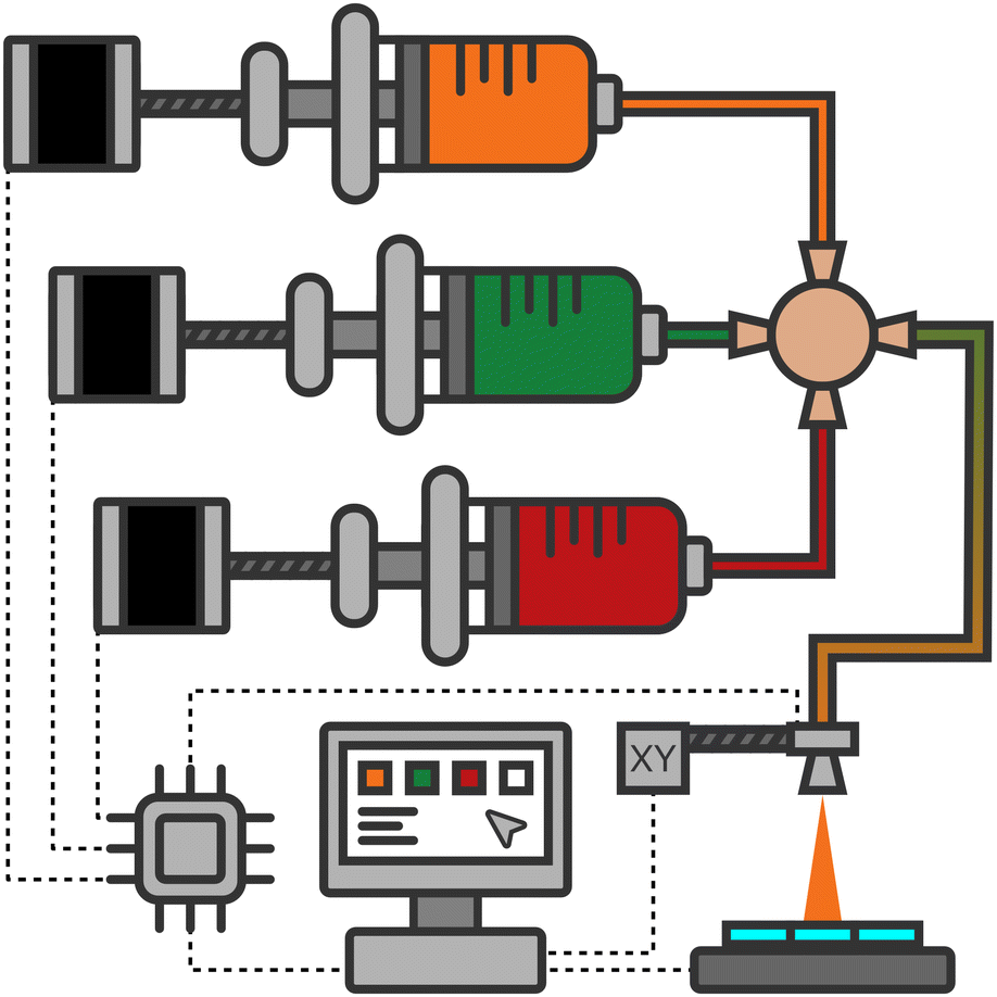 | ||
| Fig. 1 Illustration of the employed combinatorial deposition system with three custom-built syringe pumps which are controlled by a single-board computer. The solutions are mixed at a four-way connector and fed into the nozzle of the USC. | ||
Sample preparation
Established recipes for water-based spray pyrolysis of Cu2O29 and Ga2O3,30 and a modified version of the latter one are followed to prepare the precursor solutions:1. Cu: 0.025 M copper(II) acetate monohydrate (Sigma-Aldrich, 229601) and 0.050 M D-glucose (Sigma-Aldrich, G7528) in deionized water (DI water, 18 MΩ cm−1) with 8 vol% acetic acid (Sigma-Aldrich, A6283).
2. Ga: 0.040 M gallium(III) acetylacetonate (Sigma-Aldrich, 393541) in DI water with 20 vol% acetic acid.
3. Fe: 0.030 M iron(III) acetylacetonate (Sigma-Aldrich, 44920) in DI water with 20 vol% acetic acid.
The concentration of the iron precursor is reduced from the one in the Ga2O3 recipe for complete dissolution, but no further solution optimization is carried out as it is out of scope of this work.
Soda-lime glass substrates (Gerhard Menzel B.V. & Co. KG, 25 × 25 × 1.0 mm) are subsequentially cleaned in an ultrasonic bath at 50 °C for 15 min in a 1 vol% Hellmanex III washing solution (Hellma GmbH & Co. KG), DI water, and isopropanol (Carl Roth GmbH & Co. KG, 9866). After each step, the substrates are rinsed with isopropanol and dried in a nitrogen gas stream. 3 × 3 substrates are placed on a ceramic glass plate (McMaster-Carr, 84815K53) in a square arrangement as illustrated in Fig. 2 and transferred onto the hot plate of the USC which is heated to 280 °C. The utilized tool is equipped with a 120 kHz ultrasonic nozzle (Sono-Tek Corp., Impact), operating at 3.5 W in horizontal geometry, 200 mm above the substrate surface.
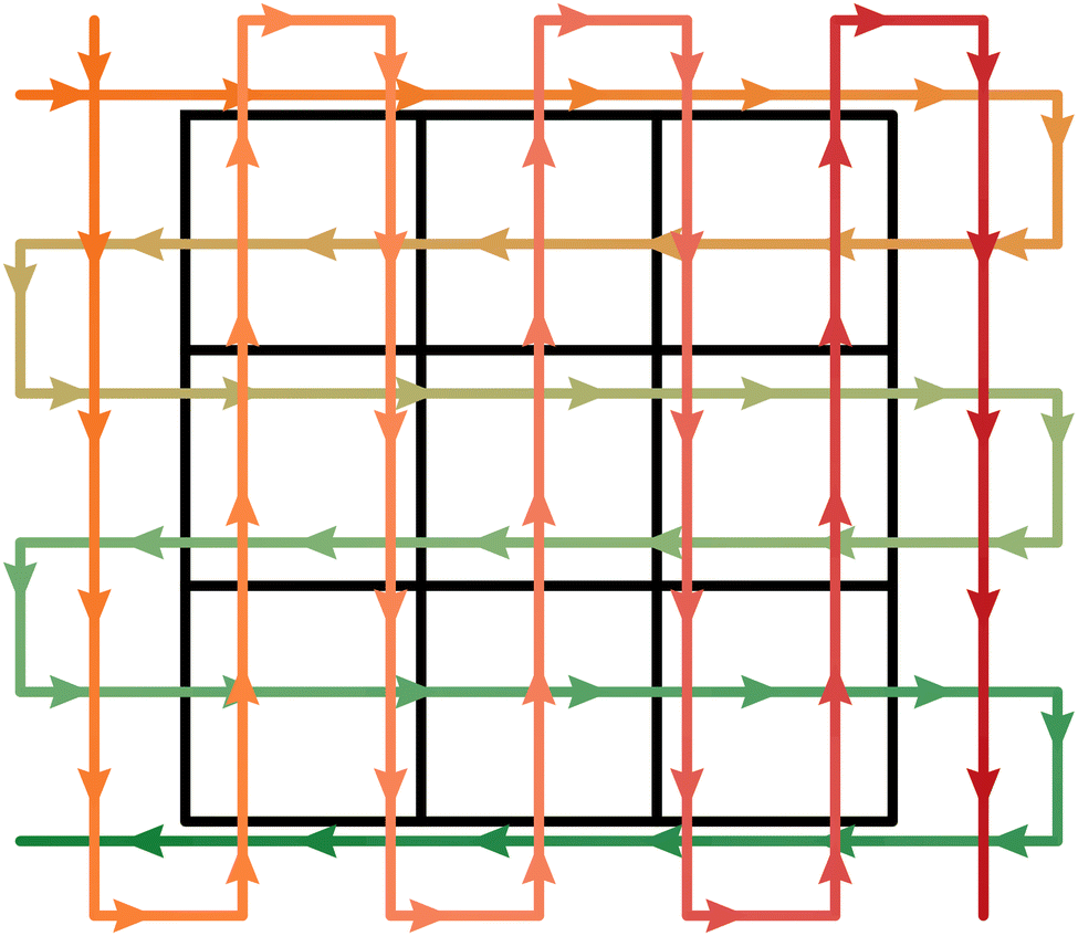 | ||
| Fig. 2 Illustration of the combinatorial spray pattern which alternates between a vertical Cu–Ga gradient (orange to green) and a horizontal Cu–Fe gradient (orange to red). The substrates are sketched in the background. Note that the number of scan lines is reduced in order to simplify the illustration. | ||
Combinatorial deposition is achieved by alternating between vertically and horizontally sprayed two-element gradients (Fig. 2). To this end, all three precursor solutions are preloaded into a separate pump of which two are running at the same time. The overall flow rate V is kept constant at 1.0 mL min−1 but the share of each operating pump changes throughout one spray cycle. For the vertical Cu–Ga gradient, the pump containing the copper precursor solution runs at 100% in the beginning, i.e., the top-left corner in Fig. 2 As the spray nozzle progresses down vertically, the flow rate of the gallium pump increases linearly while the copper pump slows down. After 25 scan lines, right before the end of the spray cycle, the gallium pump delivers the full flow rate by itself. Likewise, the horizontal Cu–Fe gradient is deposited in 27 vertical scan lines using the copper and iron pumps. An area of 110 × 95 mm is covered at a scan speed of 20 mm s−1 for a total of 40 cycles.
In order to synchronize the start of the solution gradient with the beginning of the spray cycle, the dead volume V0 between the four-way connector and the nozzle (see Fig. 1) needs to be prefilled. This is done by running the pumps prior to the nozzle movement for a precalculated time:
Sample characterization
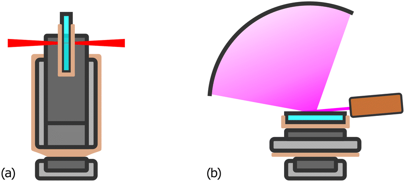
The composition of the film is determined by energy dispersive X-ray spectroscopy (EDS) using a scanning electron microscope (Carl Zeiss AG, SUPRA 40) in high vacuum equipped with a silicon drift detector (SDD, AMETEK Inc., EDAX Octane Elect Plus). All 9 samples are placed in their correct order on a purpose-built aluminium sample holder which enables automatized measurement of the whole combinatorial deposit in one run. Areas of approx. 1 mm2, each 5 mm apart, are probed for a live time of 30 s at 20 kV acceleration voltage, yielding a resolution of 15 × 15 pixels.UV-Vis transmission spectra are recorded at normal incidence from the coated side using a Fourier-transform spectrometer (FTS, Bruker Corp., Vertex 70) under ambient conditions equipped with a halogen optic lamp (Osram Licht AG, 64642 HLX). A GaP diode detector and a Si diode detector are used to cover spectral ranges of 303–588 nm and 500–1205 nm, respectively. Spatial resolution of the combinatorial film is enabled through a custom-built sample stage which moves a single substrate in horizontal and vertical direction normal to the incident beam (Fig. 3(a)). The device is made up of two miniature linear stages (Physik Instrumente GmbH & Co. KG, Q-521) and 3D printed parts. This enables semi-automatized measurement of the whole combinatorial deposit where only changing the substrate is done manually. The incident beam is focused to a spot diameter of approx. 1 mm and, as with EDS, a resolution of 15 × 15 pixels is achieved. More details can be found in S2 (ESI†). Additionally, the same instrument is used to measure the reflectance at 13° incidence non-combinatorially with one UV-Vis spectrum of each substrate.
 | ||
| Fig. 3 Illustration of the sample positioning equipment for the semi-automatized measurement of the combinatorial film. (a) for horizontal and vertical positioning in the FTS using two linear stages. (b) for polar coordinate positioning in the XRD using a rotation stage on top of a linear stage. A brass tube for collimating the beam into a circular spot is also illustrated in the right image. | ||
Structural information is obtained using a grazing incidence X-ray diffractometer (XRD, Thermo Fisher Scientific Inc., ARL Equinox 100) under ambient conditions at an angle of 5°, with Cu-Kα radiation. A similar approach as for the UV-Vis measurements is followed but had to be adapted due to the constrained space in the sample chamber of the instrument. To this end, the stage is made up of one Q-521 topped up by a rotation stage (Physik Instrumente GmbH & Co. KG, Q-632) as illustrated in Fig. 3(b). This transforms the probed locations into polar coordinates and reduces the required linear range by half. Since the incident beam is collimated by a 10 mm wide rectangular slit, a capped brass tube with a hole is used to obtain a small circular spot. A fluorescent film and a bare glass substrate with a single gold disc (≈1 mm2, 50 nm thick) sputtered on it are used to estimate the spot diameter (≈3 mm). Due to the larger measurement area, the resolution is reduced to 12 × 12 pixels. Unfortunately, only 108 of 144 measurements are usable because the beam partially reaches over the edges at the corners of each substrate. As before, the measurement of the whole combinatorial deposit is semi-automatized. More details can be found in S3 (ESI†).
As far as stability is concerned, there are no visible signs of degradation and the band gap remains virtually unchanged after storing the samples under ambient conditions for over 5 months (S4, ESI†).
Monte Carlo simulations
The NISTMonte application31 within the EPQ library of the NIST DTSA-II software package32 is used for the simulation of EDS spectra. An SDD model is populated with data from publicly available detector specifications and from measurement spectrum files (S5, ESI†). 15 × 15 pixels of the coated substrate are simulated as a layered structure with the deposited film on top of a 1 mm thick soda-lime glass layer. The EDS quantification results are used for parametrizing the top layer composition alongside the oxygen content and density which are derived from the XRD structural information. The required properties of the soda-lime glass33 are tabulated in S6 (ESI†). For each pixel, 13 spectra are generated with film thicknesses of 10, 50, 100, 200, 300, 400, 500, 600, 700, 800, 1000, 1250, and 1500 nm.Results and discussion
The combinatorial spray deposition yields a matte film with a colour gradient from dark brown to more reddish, greenish, and light brown tones in the top-right, bottom-left, and bottom-right corners, respectively (Fig. 4a). This indicates that each position on the sample area poses different compositional, structural, and/or optical properties which will be evaluated in the following sections. One full cycle of sample preparation and characterization takes approximately one working week to complete. This corresponds to a speed-up factor of 10–100 in comparison to a conventional trial-and-error approach where, realistically, 1–10 samples can be prepared and characterized in one week. Further acceleration is achieved when the (semi-)automatized tasks are parallelized which has the potential to reduce the average time by a factor of 2–4. | ||
| Fig. 4 (a) Photograph of the combinatorial film deposited on 3 × 3 soda-lime glass substrates. (b) Normalized mole fraction maps of the elemental gradients obtained by EDS measurements with standardless quantification of the as-deposited film. The values of the colour bars are the minimum, the mean, and the maximum mole fraction. | ||
Composition
Quantification of the EDS spectra is performed using a standardless eZAF correction algorithm which is provided by the proprietary analysis software of the detector (APEX™, AMETEK Inc.). The surveyed elements are fixed to O, Na, Mg, Al, Si, K, Ca, Fe, Cu, and Ga, reflecting the expected composition of the film including the substrate. In order to visualize the intended gradients, the resulting mole fractions xi of Cu, Ga, and Fe are normalized by dividing each of them by the sum of all three elements:We are aware that the ZAF model is not suited for correct quantification of stratified specimen and that there are more applicable methods,34,35 but we are mostly interested in the compositional trends and compare the different pixels of the same film with each other. Furthermore, the eZAF correction factors indicate that the high energy characteristic X-rays of Cu, Ga, and Fe are almost not affected by absorption losses (S7, ESI†). Additionally, Monte Carlo simulations predict no severe composition differences between bulk and thin film specimen if the thickness of the top layer is high enough and the results of the ZAF quantification are normalized to Cu, Ga, and Fe (S8, ESI†).
Fig. 4b depicts the results of the EDS analysis which are quite consistent with the spray pattern of the combinatorial deposition (Fig. 2). The diagonal gradient of Cu from top-left to bottom-right is formed by the overlap of the vertical Cu–Ga and horizontal Cu–Fe deposition. Note that the Ga and Fe gradients are not perfectly vertical and horizontal, but the highest amounts are found in the bottom-left and top-right corners, respectively. This is mainly a result of the differing precursor solution concentrations (S9, ESI†), but different elemental deposition rates depending on the composition of the sprayed solutions are also likely since already a change in pH can heavily influence the growth rate of a pure component.36 However, the film contains a wide variety of unique materials and the composition of the pixels is well spread-out with no severe clustering or redundant data points (S10, ESI†).
The reproducibility of the combinatorial deposition is determined by comparing the composition gradients of two equally prepared films A and B. Relative deviations of the mole fractions are calculated for each pixel with
Moreover, the composition is also fairly robust against the heat treatment with an average relative deviation of around 5.0% (S12, ESI†). On average, the non-normalized oxygen concentration decreases through annealing by 5.1 at% (S13, ESI†) which indicates the removal of oxygen by the constant nitrogen gas stream at elevated temperatures. The uptake of nitrogen is not quantified but the EDS spectra do not show a build-up of the characteristic peak.
Crystal structure
Fig. 5 depicts typical diffractograms, taken from the four corners of the combinatorial area, i.e., the regions with the highest concentrations of Cu, Ga, Fe, and Ga+Fe (see Fig. 4b). The actual positions are inset by one x and one y coordinate since the measurements of the outermost corners are not valid. Each raw data curve is pre-processed by applying a cubic baseline correction and a one-dimensional Gaussian filter as implemented in the PeakUtils37 and SciPy38 Python packages, respectively. The standard deviation for the Gaussian kernel is determined by fitting a single Gaussian function to the most prominent peak in an arbitrarily selected measurement, yielding 0.5° (S14, ESI†). Afterwards, the contribution of the substrate is removed by subtracting a smoothed measurement of bare soda-lime glass which is scaled to fit the sample diffractogram at its maximum intensity. The diffractograms of the as-deposited film consist of a single peak at 36° which coincides with the highest-intensity reflection of many possible crystal structures. Therefore, the only conclusion to be drawn from this data is a decrease of the peak prominence with decreasing Cu and increasing Ga content (S15, ESI†), indicating less crystallinity. After the heat treatment, several peaks can be observed with the most prominent still at 36° (blue line in Fig. 5 annealed). For comparison, the composition dependency of the peak prominence is evaluated again (S16, ESI†) which still shows a positive but less linear correlation with the Cu content. The negative correlation with the Ga content is less pronounced but now, the peak prominence decreases with the Fe content as well. | ||
| Fig. 5 Pre-processed diffractograms of pixels in the Cu, Ga, Fe, and Ga+Fe regions, i.e., top-left, bottom-left, top-right, and bottom-right of the combinatorial film, respectively (see Fig. 4b). The left column shows measurements from before and the right column from after the annealing heat treatment. The blue line is obtained from the solid black line by subtracting the contribution of the soda-lime glass substrate (dashed black line). | ||
The diffraction pattern of reflections at 30°, 36°, 43°, 57°, and 63° corresponds to compounds of the spinel group with Fd![[3 with combining macron]](https://www.rsc.org/images/entities/char_0033_0304.gif) m crystal structure.39 Less prominent peaks and peak shoulders can be assigned to CuO and Cu2O with C2/c and Pnm crystal structures, respectively.40,41 Compounds of the delafossite group (Rm) are also likely42,43 but cannot be isolated because the main reflection of the (10–12) plane overlaps at 36°. The peak at 26° is a measurement artifact and will not be considered in the analysis. The data quality, i.e., the poor signal-to-noise ratio and the low peak prominences, as well as the sample nature, i.e., the low crystallinity and the high defect density, do not allow the use of structure refinement approaches.44–47 Instead, a heuristic evaluation procedure is employed which is similar to the Rietveld method but much less elaborate and more robust. The diffraction patterns and densities of matching compounds (Table 1) are calculated using the Python Materials Genomics (pymatgen)48 Python package with crystal structures obtained from the Crystallography Open Database (COD).49 A Gaussian function with a standard deviation σ of 0.5° is folded on each reference pattern consisting of I intensities ιr at Θ angles θr:
m crystal structure.39 Less prominent peaks and peak shoulders can be assigned to CuO and Cu2O with C2/c and Pnm crystal structures, respectively.40,41 Compounds of the delafossite group (Rm) are also likely42,43 but cannot be isolated because the main reflection of the (10–12) plane overlaps at 36°. The peak at 26° is a measurement artifact and will not be considered in the analysis. The data quality, i.e., the poor signal-to-noise ratio and the low peak prominences, as well as the sample nature, i.e., the low crystallinity and the high defect density, do not allow the use of structure refinement approaches.44–47 Instead, a heuristic evaluation procedure is employed which is similar to the Rietveld method but much less elaborate and more robust. The diffraction patterns and densities of matching compounds (Table 1) are calculated using the Python Materials Genomics (pymatgen)48 Python package with crystal structures obtained from the Crystallography Open Database (COD).49 A Gaussian function with a standard deviation σ of 0.5° is folded on each reference pattern consisting of I intensities ιr at Θ angles θr:

For each crystal structure, the mean of C compounds is formed with
and divided by its maximum to obtain the normalized reference curve for the space group SG. Since the main contribution to the measured intensities seems to originate from a spinel crystal structure, it is evaluated first. To this end, the peaks at 30° and 57° are fit to the respective reference peaks in
![[F with combining tilde]](https://www.rsc.org/images/entities/i_char_0046_0303.gif) Fdm using PeakUtils to get the relative intensities ι and peak shifts Δθ. These two reflections correspond to the (220) and (333, 511) planes, respectively, and are selected because they do not overlap with reflections of the other reference compounds. After averaging the results, a fit reference curve is calculated:
Fdm using PeakUtils to get the relative intensities ι and peak shifts Δθ. These two reflections correspond to the (220) and (333, 511) planes, respectively, and are selected because they do not overlap with reflections of the other reference compounds. After averaging the results, a fit reference curve is calculated:The same approach is followed for the other reference curves, fitting the (111) reflection of CuO between 38° and 39° and the (111) reflection of Cu2O between 36.5° and 37.5°. A model curve is obtained as sum of all already calculated fit reference curves. Since the (111) reflection of Cu2O partially overlaps with the main peak, its ι is iteratively reduced until the intensities of model and measurement agree. Finally, if the model intensity at 36° is less than 100%, the difference is eliminated by iteratively increasing ι of the delafossite fit reference curve. In order to compare the contribution of the considered compounds only, the relative intensities are normalized with
and summarized in Table 2. The goodness of the fit is determined by forming the root mean squared error (RMSE) between model and measurement for each pixel. In this RMSE map, the average error is found to be 7% with the highest errors (up to 15%) belonging to the Ga+Fe region. The non-normalized model contains intensities above 100% in this area which indicates that the considered reference patterns do not reflect the actual compounds as well. Additionally, it is the least crystalline region because the factors of the removed soda-lime glass background are above average (S17, ESI†).
| Compound | COD | Cryst. struct. | ρ (g cm−3) | Band gap (eV) |
|---|---|---|---|---|
| a Single literature value. | ||||
| CuFe2O4 | 9012438 |
Fdm |
5.42 | 1.95 ± 0.05 |
| CuGa2O4 | 1536350 |
Fdm |
6.01 | 4.45 ± 0.05 |
| Fe3O4 | 9002320 |
Fdm |
5.36 | 2.80 ± 0.08 |
| FeGa2O4 | 1541527 |
Fdm |
5.89 | 2.45a |
| CuO | 7212242 |
C2/c | 6.52 | 3.47 ± 0.19 |
| Cu2O | 1010926 |
Pnm |
6.18 | 2.23 ± 0.05 |
| CuFeO2 | 9000015 |
Rm |
5.56 | 2.08 ± 0.07 |
| CuGaO2 | 1537363 |
Rm |
6.06 | 3.53 ± 0.07 |
| Intensity | Spinel (%) | CuO (%) | Cu2O (%) | Delafossite (%) |
|---|---|---|---|---|
| Normalized | 58.1 | 14.8 | 16.9 | 10.1 |
| Absolute | 3.9 | 48.8 | 36.1 | 11.2 |
Quantification based on the absolute intensities of the reference patterns is not possible since the phases are not expected to be stoichiometric.50 Furthermore, the resulting amounts of CuO and Cu2O (Table 2) would correspond to much higher Cu concentrations than what is measured by EDS (Fig. 4b). Since the atomic fractions in each crystal structure are limited, the amount of the phases is constrained by the overall composition. CuO and Cu2O are most likely stoichiometric and do not mix with Fe or Ga.51 A thermodynamic assessment of Cu–Fe–Ga–O cannot be referenced but Ga3+ is expected to behave like Fe3+ due to the same oxidation state and similar atomic radius. Therefore, CuFeO2 and CuGaO2 can be considered stoichiometric with respect to Cu but may interchange Fe and Ga atoms freely. This concept equally applies to the compounds with Fdm crystal structure, but, additionally, Cu2+ may be replaced with Fe2+. A model which estimates the elemental composition based on these assumptions is proposed:
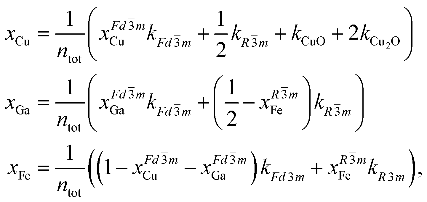
through
| ntot = kFdm + kRm + kCuO + 2kCu2O. |
m is given by xFdmCu and can be directly calculated from the scaled intensities and known Cu concentration. xFdmGa and xRmFe are unknown but cannot substantially exceed the limit set by their crystal structure. Therefore, the maps of normalized mole fractions ![[X with combining tilde]](https://www.rsc.org/images/entities/i_char_0058_0303.gif) i from the EDS quantification of the annealed film are resized to 12 × 12 pixels (S18, ESI†), scaled by max-normalization and multiplied by the maximum atomic fraction of the element in the crystal structure, i.e., 2/3 for xFdmGa and 1/2 for xRmFe. With this simplification, it is assumed that the amount of an element in a phase is maximal at its maximum concentration and distributed like the overall composition. The phase amounts of spinel, CuO, Cu2O, and delafossite are found through an exhaustive search for the κSG which minimize the RMSE between the measured and model elemental composition. This results in a far better compositional agreement (1.9% RMSE) than assuming bare spinel (12.8% RMSE), non-scaled intensities (208% RMSE), or absolute intensities (1009% RMSE) as depicted in S19 (ESI†).
i from the EDS quantification of the annealed film are resized to 12 × 12 pixels (S18, ESI†), scaled by max-normalization and multiplied by the maximum atomic fraction of the element in the crystal structure, i.e., 2/3 for xFdmGa and 1/2 for xRmFe. With this simplification, it is assumed that the amount of an element in a phase is maximal at its maximum concentration and distributed like the overall composition. The phase amounts of spinel, CuO, Cu2O, and delafossite are found through an exhaustive search for the κSG which minimize the RMSE between the measured and model elemental composition. This results in a far better compositional agreement (1.9% RMSE) than assuming bare spinel (12.8% RMSE), non-scaled intensities (208% RMSE), or absolute intensities (1009% RMSE) as depicted in S19 (ESI†).
However, the optimized average phase amounts do not consist of any Cu2O (Fig. 6a) which clearly is prevalent in the diffraction patterns. Delafossite, on the other hand, is only measured indirectly and the excess intensity may originate from crystallographic texture. Therefore, the whole procedure is repeated without considering CuFeO2 and CuGaO2. After that, the proportions of the average phase amounts from the normalized and absolute intensities in Table 2 are not changed but the compositional error is reduced to 1.4%. The resulting structure maps are shown in Fig. 6b which reveal that most of the crystalline matter has Fdm structure, as before. In both cases, CuO is significantly prevalent with over 12% in the top-left corner, reflecting the high Cu concentration. Controversially, the most Cu2O is found in the bottom-left corner, indicating that Fe has a destabilizing effect as the distribution resembles XFe in Fig. 4b. Since the standard electrode potential of Fe3+/Fe2+ is higher than that of Cu2+/Cu+, it can be assumed that Cu+ gets oxidized by Fe3+.52 Therefore, Cu2O is less likely to be formed in regions of high Fe content as opposed to spinel which seems to be promoted by Fe. Similarly, the highest amounts of delafossite are in the bottom-left corner and since it needs Cu to form, none of it is found in the Ga+Fe region. Overall, delafossite is distributed homogenously but with a lot of noise which carries over to the spinel distribution in Fig. 6a. This indicates that the solution in Fig. 6b is a better estimation because the distributions are much smoother. Ultimately, these results are only approximate and the true values can be assumed to lie between the two extremes of 0% Cu2O and 0% delafossite, i.e., 84.9–90.6% spinel, 6.5–7.8% CuO, <1.6% Cu2O, and <8.6% delafossite on average.
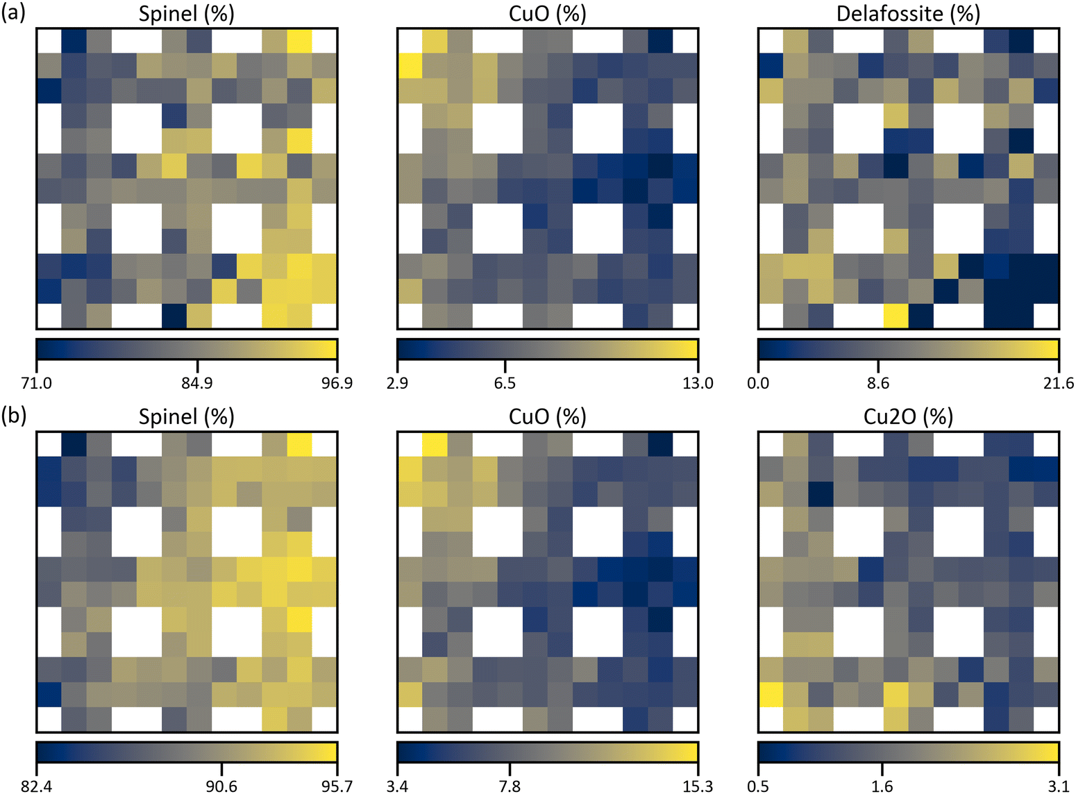 | ||
| Fig. 6 Normalized structure maps from the quantification based on the proposed composition-restricted model, (a) considering all compounds from Table 1 and (b) without considering delafossite compounds. The values of the colour bars are the minimum, the mean, and the maximum relative amount of the structure. | ||
Thickness
As already mentioned above, the EDS quantification of a thin film on a substrate is not trivial. The high penetration depth of around 1 μm leads to picking up characteristic radiation from the bottom layer. However, this can also be advantageous since the intensities of the alien signals depend on the properties of the top layer. In principle, it is possible to simultaneously obtain the composition and mass thickness of stratified specimen but it requires standards and measurements at multiple acceleration voltages.53 If the composition and density of the layers are known, one can estimate the thickness by comparing the measured spectrum with spectra obtained by Monte Carlo simulations.To this end, the normalized concentration maps i are extended by oxygen maps  which are derived from the crystal structure quantification (Fig. 6), considering both cases. Each structure map SSG is filled and resized to 15 × 15 pixels (S20, ESI†) and multiplied by its oxygen molar fraction, the results are added up. Afterwards, the concentration maps of the other elements need to be adjusted:
where

 is a 3 × C matrix of the normalized Cu, Ga, and Fe molar fractions of C compounds which correspond to a composition vector
  depending on the weight vector a. The constraints of
| ac ≥ 0 |
are satisfied by constructing
 as a diagonal matrix of rank C filled with −1,
  as a vector of C zeros,
  as a vector of C ones, and
  as a scalar 1. The problem is reframed into a quadratic program55 and solved using CVXOPT.56 The density map is obtained from the optimized weights through
with this approach, densities for simulated combinations of the considered compounds are predicted with an RMSE of 0.03 g cm−3 and a maximum error of 0.07 g cm−3 (S21, ESI†).
For each pixel, the Monte Carlo spectra are scaled by min-max-normalization and linearly interpolated between the 13 thicknesses. Every simulated detector channel is treated separately, resulting in 2000 interpolants for the relevant energy range of 0–20 keV. Using these, the thickness range of 10–1500 nm is modelled with one spectrum per nm. After min–max–normalizing the measurement, the mean squared error with each of the model spectra is formed. Finally, the thickness with the lowest error is picked, yielding the maps in Fig. 7. Error maps confirm the goodness of the fit with maximum RMSE of below 2% (S22, ESI†).
 | ||
| Fig. 7 Thickness maps of the as-deposited and annealed films, calculated based on the structure maps in Fig. 6a and b for (a and b), respectively. The values of the colour bars are the minimum, the mean, and the maximum thickness. | ||
The thickness distributions are not uniform, with a standard deviation of around 60 nm. This can be ascribed to the differing precursor solution concentrations. If only the total number of deposited atoms is considered, a non-uniform distribution with the lowest thickness in the top-left corner is predicted (S23, ESI†). Additionally, composition-dependent deposition rates and uneven overspray may contribute to further distortion. Complementary profilometer measurements of an additional spray experiment, where lines of the substrate are covered with a thin steel mask, coincide well with the obtained results (S24, ESI†). The choice of crystal structure combination (Fig. 6) does not significantly influence the result, only the spread of the values is slightly different. But the heat treatment seems to have an influence on the distribution, especially in the region of high Cu concentration. An increase of the average thickness can be attributed to an increase in density due to the higher crystallinity and lower oxygen content (S13, ESI†). Since the evaluation is based on densities of stoichiometric, crystalline compounds the thickness of the annealed film should be a better estimate for the true value. However, the thicknesses fit well within the standard deviation and the average relative deviation is around 5%.
Optical properties
Each raw spectrum pair of the UV-Vis measurements is pre-processed by cubic interpolation to reduce the amount of data points by half and obtain an even spread. The individual data curves are merged in their overlapping region by forming a weighted mean (S25, ESI†). Typical transmission spectra of the Cu, Ga, Fe, and Ga+Fe regions are shown in Fig. 8 A single photon transition with a steep slope can be observed in the Fe and Ga+Fe measurements, whereas in the Cu and Ga spectra, a second transition is indicated by a small kink at higher wavelengths. Annealing mainly amplifies the second transition in the Ga spectrum but also seems to introduce one in the Fe spectrum. This may be a consequence of the multiple phases present in the film as it coincides well with the structure maps in Fig. 6: in the Ga+Fe region, the material is almost single-phase spinel which results in a single absorption edge. But in the other regions, additional phases may contribute to the absorption behaviour. The high amount of CuO in the Cu region does not seem to affect the transmission spectrum significantly. But delafossite may be responsible for the pronounced low-energy absorption edge since it is features multi-band absorption.57 Overall, the transmission is increased through annealing. The reflectance ranges between 9 and 17% and is quite constant over the whole spectral range with a single broad peak between 500 and 750 nm (S26, ESI†).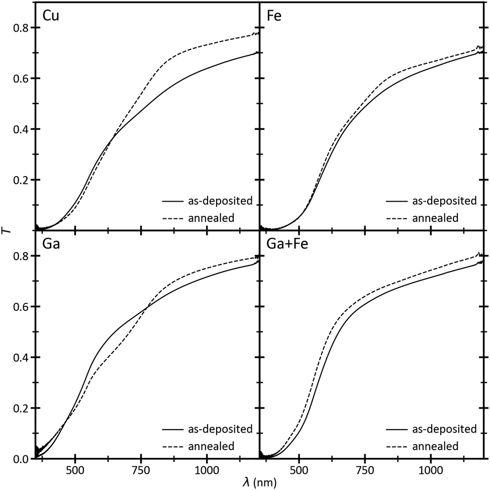 | ||
| Fig. 8 Merged transmission spectra of pixels in the Cu, Ga, Fe, and Ga+Fe regions, i.e., top-left, bottom-left, top-right, and bottom-right of the combinatorial film, respectively. | ||
The wavelength-dependent absorption coefficient α is calculated from the transmission T and reflectance R through
In order to facilitate and speed-up the evaluation of many UV-Vis measurements, an automatized routine is deployed: firstly, the fundamental absorption edge is found by searching for the largest slope of sequentially calculated linear regressions of small sections of the spectrum, i.e., numerical differentiation with finite differences.59 The algorithm starts at the highest photon energy (≈3.5
 eV) and terminates as soon as the slope does not increase for ten times in a row. The window size of the linear regression is set to 26.4 meV and 44.8 meV, and the step size is set to 1.3 meV and 4.2 meV for the as-deposited and annealed films, respectively. This ensures that the steep linear part at the high-energy end of the spectrum is used consistently for all measurements.
A baseline is then calculated by linear regression of the low-energy end (≈1.0–1.2 eV) to following.60 The strategy in ref. 60 is not strictly followed since the slope below the fundamental absorption should be used as a baseline, which is not guaranteed by setting the range of the linear regression to fixed values. The reasons behind this choice can be understood by looking at Fig. 9 which depicts the evaluation of the spectra from Fig. 8 In the case of direct transitions, there is no need for elaborate methods because the abscissa already is the correct baseline, and the conventional approach would be applicable. Still, both, the recommended strategy and the deployed automatized routine, yield the same results. In case of indirect transitions, the Tauc plot is not trivial anymore and the band gap is highly underestimated by the conventional method. Therefore, a baseline is needed which intersects the linear fit of the fundamental absorption resulting in a point whose x-coordinate is a better band gap estimation. Strictly speaking, the baseline is not set correctly in the examples shown in Fig. 9 because most of the plots include a second absorption edge in-between the two intersecting lines. The presence of additional photon transitions is already discussed for Fig. 8 and the Tauc plots agree with the statements from above. However, the edges are not clearly defined and there is no robust way of finding a better baseline, neither manually nor automatically. Moreover, the Tauc plots exhibit very pronounced band edge tailing which superposes the in-between photon transitions and the expected errors from the ambiguous baseline (<0.3eV) are smaller than the Urbach energies (S27, ESI†).
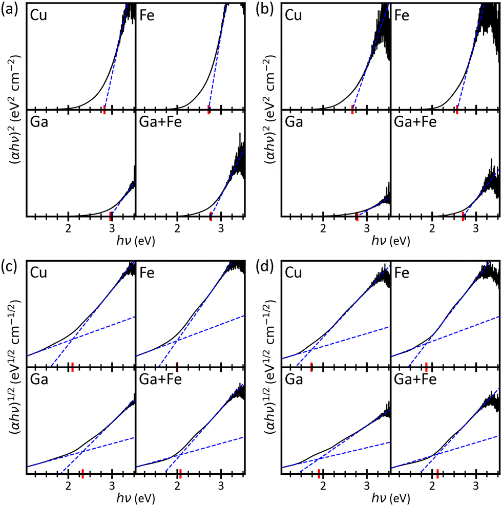 | ||
| Fig. 9 Tauc plots for the band gap evaluation of the transmission spectra in Fig. 8: (a and b) direct band gap, (c and d) indirect band gap, (a and c) as-deposited, (b and d) annealed. The band gap (red marker) is the intersection of the blue dashed lines. | ||
The results of the band gap evaluation are depicted in Fig. 10 for the as-deposited and annealed films, respectively. Prior to the heat treatment, the indirect and direct band gap distributions are very similar with differences mainly at the edges of the combinatorial area. The average indirect band gap is smaller by 0.64 eV. Annealing does not affect the direct band gap in most parts, the bottom-center changes significantly‡ but the average energy is redshifted only by 0.14 eV. The indirect band gap distribution, on the other hand, changes significantly through annealing. The RMSE is 13% larger than the average redshift of 0.22 eV as compared to 2% larger in the case of the direct band gap. Most prominently, the highest values are found in the Ga+Fe region instead of the Ga region. The differences may arise from additional absorption edges which influence the evaluation results. Like the compositional reproducibility, the band gap maps of two equally prepared films are compared. The average errors for the direct and indirect band gaps are 1.4% in both cases (S28, ESI†).
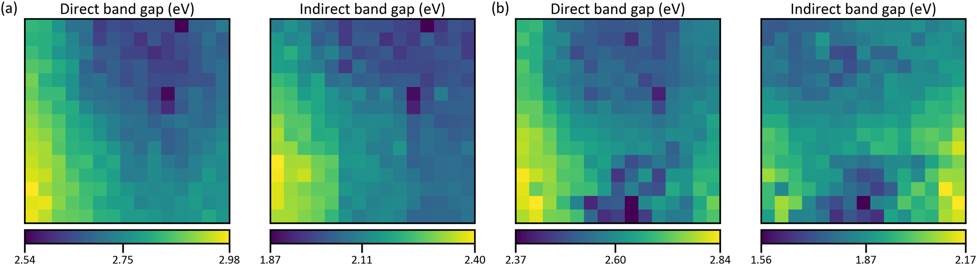 | ||
| Fig. 10 Maps of direct and indirect band gaps evaluated using the Tauc method for the (a) as-deposited film and (b) annealed film. The values of the colour bars are the minimum, the mean, and the maximum band gap energy. | ||
For comparison, a band gap map is calculated using values from references as stated in Table 1. Since indirect band gaps are not available for some compounds, only the case of direct band gaps is considered. The reference values are averaged but the ambiguity of the data gives rise to multiple means. From these, the ones where the underlying methods pose the best agreement with this work and with each other are picked. A list of all means and corresponding citations can be found in S29 (ESI†). For obtaining the calculated band gap map, the same procedure as for the density maps of the thickness estimation is followed. Hence, a result for each of the two crystal structure combinations in Fig. 6 is obtained. But only the one for Fig. 6b is shown in Fig. 11a because they are practically identical (S30, ESI†). The distribution very much resembles the map of the direct band gap in Fig. 10a with the lowest and highest energies in the Fe and Ga regions, respectively. Quantitatively, the low values match well but the high values are much lower by up to 0.89 eV and the average relative difference (Fig. 11b) is −14%. However, the simulation is based on band gap energies of stoichiometric bulk compounds as compared to the combinatorial film which consists of different mixtures of non-stoichiometric phases. Showing that the principal trends agree, confirms the evaluation of the properties on which the calculation is based, i.e., the compositional, structural, and optical analysis.
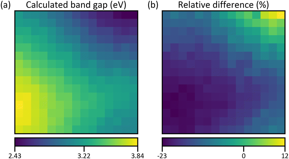 | ||
| Fig. 11 (a) Calculated direct band gap map using the reference values from Table 1 and crystal structure maps from Fig. 6b. The values of the colour bar are the minimum, the mean, and the maximum band gap energy. (b) Map of relative difference between simulated and measured direct band gap map (Fig. 10a). | ||
Data correlation
To assess the relationships between the obtained material properties, correlation matrices are calculated (Fig. 12). Each of the cells contains the linear correlation coefficient and the associated p-value61 as well as the distance correlation coefficient.62 If the latter one is much larger, a non-linear relationship can be assumed. However, this is not the case here since most of the values agree. Exceptions are the linearly non-correlated parameters, e.g., Cu and direct band gap or Ga and spinel, but the distance correlations of 0.2–0.3 are still rather unsignificant.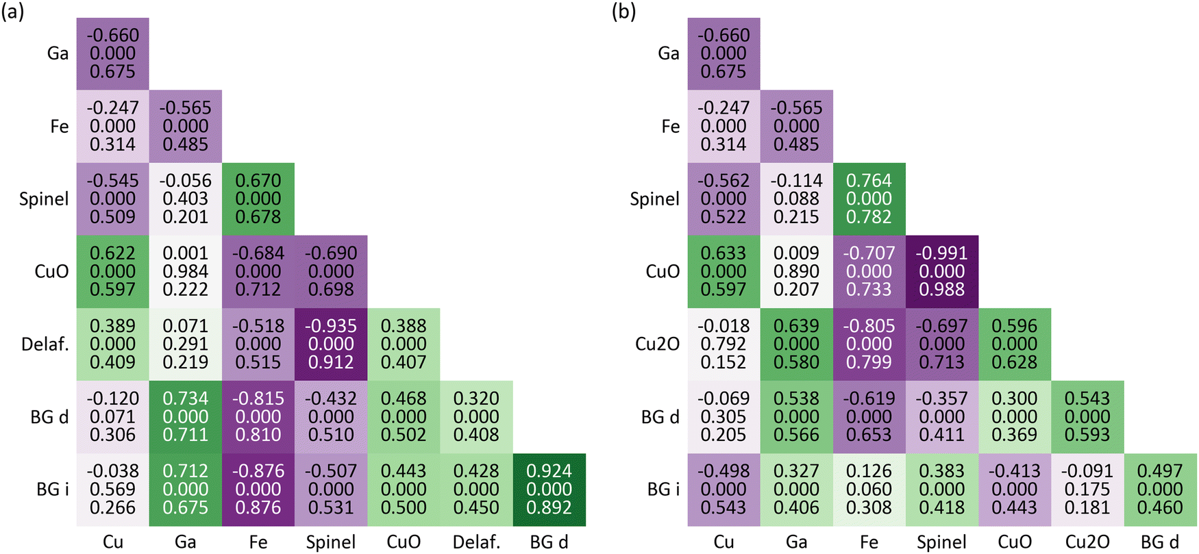 | ||
| Fig. 12 Correlation matrices for the relationships between the composition, i.e., “Cu”, “Ga”, and “Fe” for the Cu, Ga, and Fe mole fractions from Fig. 4b, the crystal structure, i.e., “Spinel”, “CuO”, “Delaf.”, and “Cu2O” for the relative amounts of spinel, CuO, delafossite, and Cu2O from Fig. 6, and “BG d” and “BG i” for the direct and indirect band gap energies from Fig. 10. (a) uses the crystal structures from Fig. 6a and band gap energies from the as-deposited film (Fig. 10a). (b) uses the crystal structures from Fig. 6b and band gap energies from the annealed film (Fig. 10b). The three values in each cell are from top to bottom: (1) linear correlation coefficient, (2) associated p-value, and (3) distance correlation coefficient. The colouring corresponds to the linear correlation coefficient with more saturated green and violet cells for higher positive and negative values, respectively. | ||
The individual parameters of the composition and the crystal structure are inherently correlated because they both add up to 1. Hence, they are only discussed with respect to the other parameters. Likewise, the thickness is completely omitted from this assessment because it is calculated based on the composition and the crystal structure. Furthermore, the band gap evaluation depends on the thickness for obtaining the absorption coefficient. For simplification, Fig. 12 does not include the correlation between the crystal structure maps from Fig. 6a and the band gap energies from the annealed film (Fig. 10b) as well as between the crystal structure maps from Fig. 6b and the band gap energies from the as-deposited film (Fig. 10a). However, this version is sufficient for the following discussion and the whole correlation matrix is depicted in S31 (ESI†).
The relative amount of spinel seems to be promoted by Fe while the other crystal structures are negatively correlated with it. This tendency most likely arises from the multivalency of the metal, i.e., Fe2+ and Fe3+, which allows it to occupy any of the cationic sites in the spinel structure. Naturally, Cu is positively correlated with CuO but, unexpectedly, it does not influence the amount of Cu2O. It is rather tied to the Ga concentration which weakens the plausibility of the crystal structure maps in Fig. 6b and supports the presence of delafossite. Still, the relative amount of Cu2O is maximal 3.1% which does not allow for definite assumptions. Overall, Ga does not have a strong effect on the crystal structures.
The band gap, on the other hand, is mainly increased with increased Ga concentration. This is already evident when looking at the band gap energies in Table 1 where the largest values belong to Ga containing components. Fe is the counteractor in this regard while Cu is not correlated with the band gap in the investigated system. The relationship between the band gap and crystal structure is typically not as strong as that with composition. When considering spinel, for instance, there appears to be a moderate negative correlation between the two, resulting in reduced band gap energies. However, it's possible that this effect is entirely due to the presence of iron, which has a tendency to form spinel and consequently decrease the energy of the band gap.
After the annealing heat treatment, the correlation coefficients of the indirect band gap change significantly. Even the unambiguous relationship with the direct band gap is lost. This is another indicator for the previously observed additional absorption edges which may be the result of amplified phase separation.
Conclusion
The presented method of using an array of three pumps for the spray deposition of a combinatorial film yields a variety of materials with distinct compositional and optical properties for a tenth to one-hundredth of the time and human labour costs in comparison to conventional approaches. It facilitates the exploration of the vast chemical space due to the highly flexible solution-based approach with reproducible results. The average batch-to-batch errors for the mole fractions of Cu, Fe, and Ga are below 4% and the band gap maps have a reproducibility of over 98%. Together with the (semi-)automatized characterization and evaluation, a platform for fast screening of relevant properties for opto-electronic materials is created. The investigated Cu–Fe–Ga–O combinatorial film is stable under ambient conditions, consists mainly of spinel phases mixed with CuO, Cu2O and/or delafossite phases, has a varying thickness in the range of 400–650 nm, and direct and indirect band gaps of 2.5–3.0 eV and 1.9–2.4 eV, respectively. In this system, the most influential parameter for the band gap is the composition with Ga and Fe having a strong positive and negative correlation, respectively. Most importantly, the developed methods are robust and can easily be adopted to other problems in the field of material research.Data availability
The files containing the processed data and associated Jupyter Notebooks for generating the presented figures are available in the ESI†: FigureData.zip. The raw data and Jupyter Notebooks for data processing are available upon request.Conflicts of interest
There are no conflicts to declare.Acknowledgements
The authors acknowledge TU Wien Bibliothek for financial support through its Open Access Funding Programme.Notes and references
- A. Aspuru-Guzik and K. Persson, Materials Acceleration Platform: Accelerating Advanced Energy Materials Discovery by Integrating High-Throughput Methods and Artificial Intelligence, Canadian Institute for Advanced Research, Toronto, 2018 Search PubMed.
- J. Schmidt, M. R. Marques, S. Botti and M. A. Marques, npj Comput. Mater., 2019, 5, 1–36 CrossRef.
- W. F. Maier, K. Stöwe and S. Sieg, Angew. Chem., Int. Ed., 2007, 46, 6016–6067 CrossRef CAS PubMed.
- S. S. Mao and P. E. Burrows, J. Materiomics, 2015, 1, 85–91 CrossRef.
- P. J. McGinn, ACS Comb. Sci., 2019, 21, 501–515 CrossRef CAS PubMed.
- A. Ludwig, npj Comput. Mater., 2019, 5, 1–7 CrossRef.
- J. M. Gregoire, L. Zhou and J. A. Haber, Nat. Synth., 2023, 1–12 Search PubMed.
- P. S. Patil, Mater. Chem. Phys., 1999, 59, 185–198 CrossRef CAS.
- S. Rühle, H. N. Barad, Y. Bouhadana, D. A. Keller, A. Ginsburg, K. Shimanovich, K. Majhi, R. Lovrincic, A. Y. Anderson and A. Zaban, Phys. Chem. Chem. Phys., 2014, 16, 7066–7073 RSC.
- M. Pavan, S. Rühle, A. Ginsburg, D. A. Keller, H.-N. Barad, P. M. Sberna, D. Nunes, R. Martins, A. Y. Anderson, A. Zaban and E. Fortunato, Sol. Energy Mater. Sol. Cells, 2015, 132, 549–556 CrossRef CAS.
- K. Kardarian, D. Nunes, P. Maria Sberna, A. Ginsburg, D. A. Keller, J. Vaz Pinto, J. Deuermeier, A. Y. Anderson, A. Zaban, R. Martins and E. Fortunato, Sol. Energy Mater. Sol. Cells, 2016, 147, 27–36 CrossRef CAS.
- A. Ginsburg, D. A. Keller, H.-N. Barad, K. Rietwyk, Y. Bouhadana, A. Anderson and A. Zaban, Thin Solid Films, 2016, 615, 261–264 CrossRef CAS.
- K. Majhi, L. Bertoluzzi, K. J. Rietwyk, A. Ginsburg, D. A. Keller, P. Lopez-Varo, A. Y. Anderson, J. Bisquert and A. Zaban, Adv. Mater. Interfaces, 2016, 3, 1500405 CrossRef.
- S. Panigrahi, D. Nunes, T. Calmeiro, K. Kardarian, R. Martins and E. Fortunato, ACS Comb. Sci., 2017, 19, 113–120 CrossRef CAS PubMed.
- C. Chen, Y. Zhao, S. Lu, K. Li, Y. Li, B. Yang, W. Chen, L. Wang, D. Li, H. Deng, F. Yi and J. Tang, Adv. Energy Mater., 2017, 7, 1700866 CrossRef.
- J. S. Compton, C. A. Peterson, D. Dervishogullari and L. R. Sharpe, ACS Comb. Sci., 2019, 21, 489–499 CrossRef CAS PubMed.
- S. Tirosh, N. Aloni, S. Meir, A. Zaban, D. Cahen and D. Golodnitsky, ACS Comb. Sci., 2020, 22, 18–24 CrossRef CAS PubMed.
- S. Tirosh, N. Aloni, D. Cahen and D. Golodnitsky, Solid State Ionics, 2022, 386, 116050 CrossRef CAS.
- A. U. Vijayakumar, N. Aloni, V. T. Veettil, G. Rahamim, S. S. Hardisty, M. Zysler, S. Tirosh and D. Zitoun, ACS Appl. Energy Mater., 2022, 5, 4017–4024 CrossRef CAS.
- J. N. Cawse, D. Olson, B. J. Chisholm, M. Brennan, T. Sun, W. Flanagan, J. Akhave, A. Mehrabi and D. Saunders, Prog. Org. Coat., 2003, 47, 128–135 CrossRef CAS.
- V. Preethi and S. Kanmani, Mater. Sci. Semicond. Process., 2013, 16, 561–575 CrossRef CAS.
- S. Saadi, A. Bouguelia and M. Trari, Renewable Energy, 2006, 31, 2245–2256 CrossRef CAS.
- H. Gao, S. Liu, Y. Li, E. Conte and Y. Cao, Energies, 2017, 10, 1787 CrossRef.
- C. G. Read, Y. Park and K.-S. Choi, J. Phys. Chem. Lett., 2012, 3, 1872–1876 CrossRef CAS PubMed.
- Q.-L. Liu, Z.-Y. Zhao, R.-D. Zhao and J.-H. Yi, J. Alloys Compd., 2020, 819, 153032 CrossRef CAS.
- K. Ueda, T. Hase, H. Yanagi, H. Kawazoe, H. Hosono, H. Ohta, M. Orita and M. Hirano, J. Appl. Phys., 2001, 89, 1790 CrossRef CAS.
- Q.-M. Zhao, Z.-Y. Zhao, Q.-L. Liu, G.-Y. Yao and X.-D. Dong, J. Phys. D: Appl. Phys., 2020, 53, 135102 CrossRef CAS.
- D. B. Khadka and J. Kim, J. Phys. Chem. C, 2015, 119, 1706–1713 Search PubMed.
- N. Plankensteiner, W. Kautek and T. Dimopoulos, ChemNanoMat, 2020, 6, 663–671 CrossRef CAS.
- N. Winkler, R. Adhi Wibowo, W. Kautek, G. Ligorio, E. J. W. List-Kratochvil and T. Dimopoulos, J. Mater. Chem. C, 2019, 7, 69–77 RSC.
- N. W. M. Ritchie, Surf. Interface Anal., 2005, 37, 1006–1011 CrossRef CAS.
- N. W. M. Ritchie, Microsc. Microanal., 2009, 15, 454–468 CrossRef CAS PubMed.
- Thermo Scientific Microscope slides, https://assets.thermofisher.com/TFS-Assets/APD/brochures/objekttraeger_uk_0715_0209.pdf, (accessed 22 November 2022).
- D. F. Kyser and K. Murata, IBM J. Res. Dev., 1974, 18, 352–363 CAS.
- J.-L. Pouchou and F. Pichoir, in Electron Probe Quantitation, ed. K. F. J. Heinrich and D. E. Newbury, Springer US, Boston, MA, 1991, pp. 31–75 Search PubMed.
- F. Caillaud, A. Smith and J.-F. Baumard, J. Am. Ceram. Soc., 1993, 76, 998–1002 CrossRef CAS.
- L. H. Negri and C. Vestri, lucashn/peakutils Zenodo, 2017.
- P. Virtanen, R. Gommers, T. E. Oliphant, M. Haberland, T. Reddy, D. Cournapeau, E. Burovski, P. Peterson, W. Weckesser, J. Bright, S. J. van der Walt, M. Brett, J. Wilson, K. J. Millman, N. Mayorov, A. R. J. Nelson, E. Jones, R. Kern, E. Larson, C. J. Carey, İ. Polat, Y. Feng, E. W. Moore, J. VanderPlas, D. Laxalde, J. Perktold, R. Cimrman, I. Henriksen, E. A. Quintero, C. R. Harris, A. M. Archibald, A. H. Ribeiro, F. Pedregosa, P. van Mulbregt and SciPy 1.0 Contributors, Nat. Methods, 2020, 17, 261–272 CrossRef CAS PubMed.
- E. J. W. Verwey and E. L. Heilmann, J. Chem. Phys., 1947, 15, 174–180 CrossRef CAS.
- D. P. Volanti, M. O. Orlandi, J. Andrés and E. Longo, CrystEngComm, 2010, 12, 1696–1699 RSC.
- M. C. Neuburger, Z. Physik, 1931, 67, 845–850 CrossRef CAS.
- A. Pabst, Am. Mineral., 1938, 23, 175–176 Search PubMed.
- H. Hahn and C. De Lorent, Z. Anorg. Allg. Chem., 1955, 279, 281–288 CrossRef CAS.
- H. M. Rietveld, J. Appl. Cryst., 1969, 2, 65–71 CrossRef CAS.
- L. B. McCusker, R. B. Von Dreele, D. E. Cox, D. Louër and P. Scardi, J. Appl. Cryst., 1999, 32, 36–50 CrossRef CAS.
- G. S. Pawley, J. Appl. Cryst., 1981, 14, 357–361 CrossRef CAS.
- A. Le Bail, H. Duroy and J. L. Fourquet, Mater. Res. Bull., 1988, 23, 447–452 CrossRef CAS.
- S. P. Ong, W. D. Richards, A. Jain, G. Hautier, M. Kocher, S. Cholia, D. Gunter, V. L. Chevrier, K. A. Persson and G. Ceder, Comput. Mater. Sci., 2013, 68, 314–319 CrossRef CAS.
- S. Gražulis, A. Daškevič, A. Merkys, D. Chateigner, L. Lutterotti, M. Quirós, N. R. Serebryanaya, P. Moeck, R. T. Downs and A. Le Bail, Nucleic Acids Res., 2012, 40, D420–D427 CrossRef PubMed.
- X-Ray reflexions from dilute solid solutions, https://royalsocietypublishing.org/doi/epdf/10.1098/rspa.1947.0064, (accessed 16 December 2022).
- A. V. Khvan, O. B. Fabrichnaya, G. Savinykh, R. Adam and H. J. Seifert, J. Phase Equilib. Diffus., 2011, 32, 498–511 CrossRef CAS.
- A. Bard, Standard Potentials in Aqueous Solution, Routledge, New York, 2017 Search PubMed.
- J. L. Pouchou and F. Pichoir, Scanning Microsc., 1993, 1993, 167–189 Search PubMed.
- X.-Y. Cui, S. P. Ringer, G. Wang and Z. H. Stachurski, J. Chem. Phys., 2019, 151, 194506 CrossRef PubMed.
- S. P. Boyd and L. Vandenberghe, Convex optimization, Cambridge University Press, Cambridge, UK, New York, 2004 Search PubMed.
- M. S. Andersen, J. Dahl and L. Vandenberghe, CVXOPT: Python Software for Convex Optimization (v1.3.0), 2022.
- S. Vojkovic, J. Fernandez, S. Elgueta, F. E. Vega, S. D. Rojas, R. A. Wheatley, B. Seifert, S. Wallentowitz and A. L. Cabrera, SN Appl. Sci., 2019, 1, 1322 CrossRef.
- J. Tauc, R. Grigorovici and A. Vancu, Phys. Status Solidi B, 1966, 15, 627–637 CrossRef CAS.
- R. L. Burden, J. D. Faires and A. M. Burden, Numerical Analysis, Cengage Learning, Boston, 2015 Search PubMed.
- P. Makuła, M. Pacia and W. Macyk, J. Phys. Chem. Lett., 2018, 9, 6814–6817 CrossRef PubMed.
- D. Freedman, R. Pisani and R. Purves, Statistics: Fourth International Student Edition, W. W. Norton & Company, New York, 2007 Search PubMed.
- G. J. Székely and M. L. Rizzo, J. Stat. Plan. Inference, 2013, 143, 1249–1272 CrossRef.
Footnotes |
| † Electronic supplementary information (ESI) available: Supplementary information (PDF), Electronics schematic (PDF), FigureData.zip. See DOI: https://doi.org/10.1039/d3ma00136a |
| ‡ This anomaly may not be reproducible and could originate from the particular heat treatment, as the bottom row of three substrates has significantly higher Urbach energies. But further investigation is not in scope of this work since it is rather focussed on showing the ability of detecting such anomalies. |
| This journal is © The Royal Society of Chemistry 2023 |