DOI:
10.1039/D3MA00133D
(Paper)
Mater. Adv., 2023,
4, 2659-2666
Facile synthesis of ternary MXene nanocomposites as an electrode for supercapacitive applications†
Received
20th March 2023
, Accepted 17th May 2023
First published on 19th May 2023
Abstract
Supercapacitors (SCs) are particularly appealing for building a new generation of energy storage devices considering their low cost and unique features. Thus, we present a facile and scalable approach to fabricate and engineer ternary composite electrodes composed of MXene and metal oxides (MnO2 and CuO) to develop supercapacitors with high gravimetric capacitances. Firstly, a series of CuO on FSSM (Flexible Stainless Steel Mesh) CuO@FSSM thin films were synthesized by SILAR, and subsequently, a MnO2/MXene composite (MMC) was deposited on the CuO@FSSM films by a simple cost-effective R-CBD method to synthesize CuO@MMC. The optimized CuO20@MMC ternary composite electrode showed a gravimetric capacitance of 924.16 F g−1 at 2 mA cm−2. Furthermore, this ternary composite electrode was employed in an asymmetric supercapacitor device (ASC) delivering 25.54 F g−1 specific capacitance with a capacitance retention of 87.27% over 2000 cycles. Thus, this method and the results are promising to fabricate advanced electrode materials for high-performing supercapacitors combining MXene and metal oxides.
1. Introduction
The increased energy demand for changing lifestyles, prosperity, expanding population, and industrialization have sparked the development of newer, efficient, and sustainable energy technologies. Consequently, energy-storage systems have drawn a lot of interest due to the rising energy consumption and environmental crisis. In particular, flexible-structured supercapacitors (SCs) are undeniably appealing because of their prospective uses in portable electronics, which are advantageous for integrating with power conversion devices like wearable displays and solar cells, among others. SCs, due to their increased specific power density, reversibility, quick charge/discharge rate, and prolonged cyclability have evolved over the past several decades into a clean and efficient energy storage and conversion technology. Recently, the drive toward miniaturization of gadgets (micro-nano) has drawn attention to developing next-generation smart, wearable, flexible, and extensible electronic devices-supercapacitors encapsulated with high-density materials. Based on the mechanism, SCs are mainly classified into electrical double-layer capacitors (EDLCs) and pseudocapacitive capacitors. In EDLCs, electrical charge develops at the electrode/electrolyte interface (Gouy–Chapman–Stern–Grahame model). On the other hand, the electric charge develops due to the utilization of redox reactions in pseudocapacitors, wherein, the performance of SCs is usually attributed to the electrode materials. In EDLC, carbon materials viz. activated carbon, carbon nanotubes, carbon fibers, graphene, graphene/carbon nanotubes, etc., usually with a large accessible surface area are employed.1–3 However, their practical applicability in EDLCs is hindered because of their inherently lower energy storage capacity. Similarly, the transition metal oxides and conducting polymers have not achieved the envisaged high theoretical capacitance in experiments, which is attributed to their poor electrical conductivity.4,5
To circumvent the above issue, significant efforts are being devoted to modifying the surface of carbon materials with transition metal oxides for achieving a high specific capacitance (Csp) and excellent electrochemical performance of supercapacitors. On the other hand, the new class of 2D transition metal carbides (MXenes) discovered a decade ago has received a massive response due to their promising properties such as large specific surface area, metallic conductivity, hydrophilic character (–OH, –O, –F terminated surface), interesting mechanical properties, and morphology similar to graphene.6,7 These materials are expressed as Mn+1XnTx, in which the transition metal is represented as M, C and/or N as X, and surface functional groups (–OH, –O, –F) as Tx. MXene electrodes made using the traditional approach have lower gravimetric Csp because the MXene is terminated with OH, O, and F groups during exfoliation and etching. In addition to the inevitable self-stacking of MXene sheets, which results in undesired features like limited surface area and less accessible active sites, this causes the properties of MXene to change from metallic to semiconducting. MXenes are therefore seen as potentially valuable auxiliary materials that can alter the conductivity of the active components, and hence, improve the electrochemical performance when building devices with other materials like metal oxides.8–11 The electrochemical energy storage properties of MXenes can be enhanced by decorating the MXene with pseudocapacitive materials like metal oxides.
Metal oxides such as NiO,12 CuO,13 RuO2,14 Fe3O4,15 Fe2O3,16 MnO2,17 Co3O4,18 and V2O519 are already being explored as electrodes in supercapacitors demonstrating potential leads. Even though RuO2 and IrO2 are well-studied as pseudocapacitive electrode materials, tragically their high-cost limits their commercial applications. Thus, cost-effective alternatives like CuO, MnO2, Co3O4, ZnFe2O4, etc. are being sought for their possible applications. Interestingly, copper oxide (CuO) and manganese dioxide (MnO2) are abundant, low-cost, non-toxic, easy to prepare, and exhibit good electrochemical performance, and thus, are looked upon as promising candidates as a pseudocapacitive material. It is envisaged that the three components/ternary composite would exhibit a synergistic effect enhancing the performance of the supercapacitor.
The ternary polypyrrole/graphene oxide/zinc oxide composite supercapacitor electrodes were synthesized and their gravimetric capacitance was calculated to be 94.6 F g−1 at 1 A g−1 using GCD curves.20 Cai et al. synthesized an MXene-CNT/PANI ternary composite electrode and demonstrated enhanced Csp of 429.4 F g−1 at 1 A g−1, which was better than the individual compound in the ternary material. These studies highlight the significance and design of multi-component composite electrodes for enhancing supercapacitor performance. With this motivation, herein this work, a facile and scalable synthesis of a ternary composite (MXene doped with MnO2 and CuO) as an electrode is developed for enhancing the gravimetric capacitances. Firstly, a series of CuO@FSSM thin films were synthesized by SILAR, and in the subsequent step, the MnO2/MXene composite (MMC) is deposited over it by a simple and cost-effective R-CBD method to form CuO@MMC. The crystal structure, morphology, and surface state properties of the CuO@MMC electrode were investigated in detail. Furthermore, the electrochemical properties of the CuO@MMC nanocomposite series were studied using CV, GCD, and EIS techniques. The synthesized ternary nanocomposite (CuO@MMC) electrode enhances the Csp and long-term cycling stability revealing it to be a potential electrode for SC applications.
2. Experimental section
2.1. Materials and chemicals
KMnO4, MnSO4·H2O, CuSO4·5H2O, NaOH (Sigma Aldrich), Flexible stainless steel mesh (FSSM) substrate with 300 mesh size (Micro Mesh India Private Limited), titanium aluminium carbide (Ti3AlC2; 200 mesh) 11 Technology (China), 1-methyl-2-pyrrolidone (NMP, Reagent Plus, 99%), poly(vinylidene fluoride) (PVDF, MW: 534![[thin space (1/6-em)]](https://www.rsc.org/images/entities/char_2009.gif) 000 g mol−1) (Sigma Aldrich, USA) and Super P carbon black (IMERYS Graphite & Carbon, Canada) were used as received without additional purification.
000 g mol−1) (Sigma Aldrich, USA) and Super P carbon black (IMERYS Graphite & Carbon, Canada) were used as received without additional purification.
2.2. Synthesis of Ti3C2Tx powder
Multilayered Ti3C2Tx powder was synthesized by etching MAX phase Ti3AlC2 using aqueous hydrofluoric acid (HF). It is worth noting that HF-based solutions cannot be used in glassware, and handling HF needs more caution than other acids. Thus, appropriate care was taken while handling HF. 1 g of Ti3AlC2 was slowly and carefully added in 10 mL of HF (38%) solution (over the period for 10 min) under constant stirring for 5 h at 35 °C to avoid overheating. The mixture was then rinsed five times with deionized water (DI) to remove any remaining HF acid, followed by centrifugation at 3500 rpm for 5 min until the pH of the supernatant reached 6. After drying the crude powder at 80 °C for 12 h in an N2 environment, the final multilayered Ti3C2Tx powder was formed with an increased interlayer spacing of MXenes21,22 (labelled as MX).
| TI3AlC2 + 3HF → Ti3C2 + AlF3 + 3/2H2 |
The working electrode was prepared by mixing the active electrode material MX, acetylene black, and PVDF with a mass ratio of 80:10:10 to form a slurry by using NMP. Acetylene black was added to create a conductive network in between the MXene sheets.23 The slurry was then coated onto FSSM by screen printing. The 3 × 1 cm (l × b) FSSM was ultrasonically cleaned in a detergent soap solution for 30 min and rinsed with deionized water and acetone, followed by drying before its every use.
2.3. Synthesis of CuO thin film
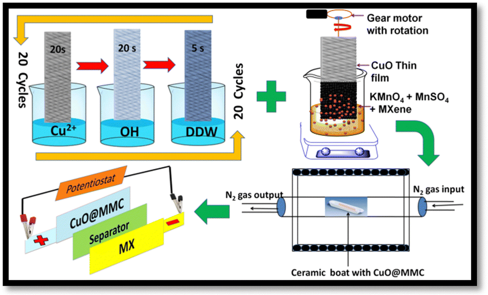
The SILAR method was used to produce CuO thin films. In a typical synthesis process, 0.05 M CuSO4·5H2O (cationic) and 0.1 M NaOH (anionic) precursors were used. The pH of the cationic precursor was maintained at ∼10 by slowly adding ammonia (NH3) solution resulting in the formation of cupric-ammonium complex [Cu(NH3)4]2+. The SILAR process involving three steps in a cycle is illustrated in Fig. 1. Typically, the precleaned FSSM substrate was sequentially immersed in the cationic precursor (20 s for adsorbing Cu2+ ions on the substrate surface) and in the anionic precursor (20 s for reacting OH− ions with copper ions forming Cu(OH)2), and finally rinsed with double distilled water (DDW) for 5 s to remove loosely bound ions. The SILAR process was optimized by varying the number of cycles to 20, 30, and 40, and the resulting electrodes were labelled CuO20@FSSM, CuO30@FSSM, and CuO40@FSSM, respectively. The electrodes were dried at 60 °C (12 h) and thereafter annealed in the furnace at 450 °C (2 h).
 |
| | Fig. 1 Schematic of the synthesis of CuO@MMC. | |
2.4. Synthesis of the CuO@MMC(MnO2/MXene) composite thin film
The CuO20@FSSM, CuO30@FSSM, and CuO40@FSSM films were directly used to deposit the MnO2/MXene composite (MMC). In a typical process, the MMC thin films were directly grown on CuO20@FSSM, CuO30@FSSM, and CuO40@FSSM by the R-CBD method using 25 mL of precursor solutions containing 0.3 M KMnO4, 0.1 M MnSO4·H2O and 0.4 g of as prepared Ti3C2Tx MXene powder. The MXene ultrasonically dispersed in 25 mL DI water for 30 min at room temperature was mixed with the above precursor solution under constant stirring for 5 min to form a homogenous mixture. The CuO20@FSSM, CuO30@FSSM, and CuO40@FSSM substrate immersed in a bath solution was rotated at 55 rpm for 3 h with a gear motor. After 2 h, the substrates were removed, washed with deionized water to remove loosely bound and physically adsorbed particles, and then dried at room temperature. The CuO@MnO2/MXene composite (MMC) films were then labelled as CuO20@MMC, CuO30@MMC, and CuO40@MMC, respectively, and were eventually calcined in a tube furnace under nitrogen at 450 °C for 2 h. Furthermore, the films were characterized for structural, morphological, and electrochemical properties.
2.5. Materials characterization
X-ray diffraction (XRD, Bruker D2 phaser X-ray diffractometer, CuKα1, 1.5406 Å) spectra, Fourier transform infrared (FTIR, Bruker Alfa Spectrometer, powder sample with KBr pellet) spectra, and scanning electron microscopy (SEM; JEOL-JSM-6360) images of MMC thin films were recorded for structural and morphological study. EDS (JEOL, JEM-2100F) was used for elemental mapping and X-ray photoelectron spectroscopy (XPS, VG Multilab ESCA, USA, Mg Kα source, 1.254 keV) analysis was performed for studying the elemental composition. The surface area was measured by a Brunauer–Emmett–Teller (BET, Quantachrome NOVA 1000e, USA) analyzer.
2.6. Electrochemical measurements
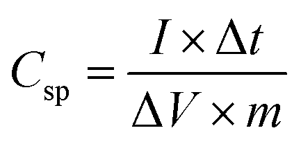
All the electrochemical studies like cyclic voltammetry (CV), galvanostatic charge–discharge (GCD), and electrochemical impedance spectroscopy (EIS) were performed using a CHI 608E Electrochemical Analyser with the standard three-electrode system. CuO20@FSSM, CuO30@FSSM, and CuO40@FSSM acted as the working electrode in 1 M KOH and CuO20@MMC, CuO30@MMC, and CuO40@MMC acted as the working electrode in 1 M Na2SO4 aqueous electrolyte with graphite (counter electrode) and a saturated Ag/AgCl (reference electrode) at RT. The CV curves were recorded vs. saturated Ag/AgCl electrode in the optimized potential window range (0 to 0.6 V) with varying scan rates (10–100 mV s−1) for CuO20@FSSM, CuO30@FSSM, and CuO40@FSSM, and in the optimized potential window range −1 to 1.2 V with varying scan rates (25-125 mV s−1) for CuO20@MMC, CuO30@MMC, and CuO40@MMC. GCD curves at the various current densities were recorded, and Csp was calculated following eqn (1) reported in the literature.24 EIS measurements (frequency range of 1000 kHz to 1 Hz) were recorded at an open circuit potential with an interval of 5 mV.| |  | (1) |
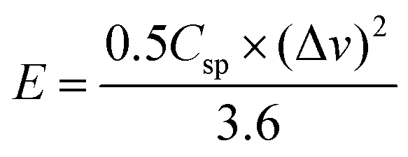
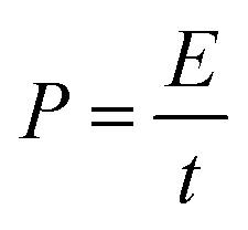
where Csp (specific capacitance, F g−1), I (response current, mA cm−2), Δt (discharge time, s), m (mass of the electrode recorded using the weight difference method, g), and ΔV (potential range, V). The power density (P, kW kg−1) and energy density (E, W h kg−1) were calculated from the GCD curves using eqn (2) and (3) given by:| | 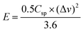 | (2) |
| |  | (3) |
where ΔV (applied potential window, V), and t (discharge time, s).
2.7. CuO20@MMC//MX Assembly
The CuO20@MMC//MX solid-state ASC device was constructed by employing CuO20@MMC thin film (positive electrode), cellulose filter paper (separator sandwiched between the two electrodes), and MX thin film (negative electrode). The device assembly was soaked in PVA–KOH gel electrolyte and then left overnight at room temperature for natural drying. The PVA–KOH gel electrolyte (dissolving 5 g PVA and 4 g KOH in 80 mL DDW) was synthesized following previous work in the literature.25,26 The assembly of the ASC device was press compressed at 6 MPa pressure to establish adequate contact between the electrode material and the electrolyte.
3. Results and discussion
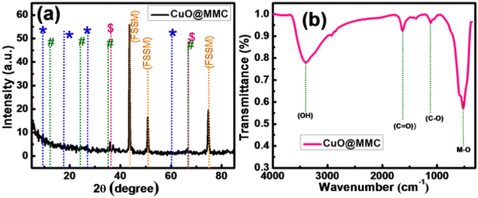
It is expected that the porous structure of CuO20@MMC would be advantageous during the fast ion adsorption–desorption process favouring reversible redox reactions and consequently enhancing the supercapacitor performance.27 To further support the observations, comparative crystal structure characterization of CuO, CuO20@MMC, CuO30@MMC, and CuO40@MMC thin films was carried out by XRD, as shown in (ESI†) S1(a). The CuO XRD peaks at 35.54, 38.71, 48.72, 58.26, 61.52, 66.22, and 68.12° could be indexed to the (111), (11−1), (20−2), (202), (11−3), (31−1), and (220) planes of the monoclinic CuO (JCPDS48-1548).28 Furthermore, the additional peaks observed at 2θ of 43.5, 50.2, and 75° are attributed to the (FSSM) mesh substrate. The XRD pattern of the optimized sample CuO20@MMC is shown in Fig. 2(a). In the XRD spectrum, the diffraction peaks at 9.1, 18.2, 27.5, and 60.7° correspond to the crystalline plane of Ti3C2 and are in good agreement with the previous result in the literature marked by (*) sign.29 In the XRD spectrum of CuO20@MMC, the diffraction peak of the Ti3C2 (002) plane moves to a lower 2θ value (from 9.5 to 9.1°). This is due to increased d-spacing resulting from the structural expansion produced by etching and Al replacement with –F and –OH/![[double bond, length as m-dash]](https://www.rsc.org/images/entities/char_e001.gif) O termination groups.30 The removal of the characteristic peak at 39° (104) of the raw material MAX phase Ti3AlC2 when it was etched by the concentrated hydrofluoric acid solution at room temperature verified the etching of Al from MAX phase Ti3AlC2. This suggests that the Al layer was effectively exfoliated and that the 2D Ti3C2Tx MXene has formed. Furthermore, new XRD peaks for Ti3C2F2 were found at ∼18.2°, indicating that F was introduced into the Ti3C2Tx MXenes interlayer.31 Along with this a new peak detected at ∼27.5° was assigned to Ti3C2(OH)2.32 These results show that the Ti3C2Tx surface is terminated with –OH, and –F functional groups after HF etching. Furthermore, the peaks were in good agreement with the literature. The (#) sign indicates the broad and weak reflection peaks and corresponding planes observed at about 12 (001), 26 (002), 37 (111), and 66 (002) degrees of δ-MnO2, respectively.33 The XRD pattern was in good agreement with the JCPDS card no. 80-1098652. Furthermore, the weak peaks at 35.2, 48.6, and 58.2° are attributed to the (111), (20−2), and (202) planes of CuO, respectively (labeled as $). On the other hand, the peaks originating from CuO were suppressed as CuO was covered with MnO2/MXene. The FSSM mesh substrate is accountable for additional stainless steel peaks that were seen at 2θ of 43.5, 50.2, and 75°. These characteristic peaks indicate that the synthesized thin films belong to CuO20@MMC (MnO2/MXene composite) structure.
O termination groups.30 The removal of the characteristic peak at 39° (104) of the raw material MAX phase Ti3AlC2 when it was etched by the concentrated hydrofluoric acid solution at room temperature verified the etching of Al from MAX phase Ti3AlC2. This suggests that the Al layer was effectively exfoliated and that the 2D Ti3C2Tx MXene has formed. Furthermore, new XRD peaks for Ti3C2F2 were found at ∼18.2°, indicating that F was introduced into the Ti3C2Tx MXenes interlayer.31 Along with this a new peak detected at ∼27.5° was assigned to Ti3C2(OH)2.32 These results show that the Ti3C2Tx surface is terminated with –OH, and –F functional groups after HF etching. Furthermore, the peaks were in good agreement with the literature. The (#) sign indicates the broad and weak reflection peaks and corresponding planes observed at about 12 (001), 26 (002), 37 (111), and 66 (002) degrees of δ-MnO2, respectively.33 The XRD pattern was in good agreement with the JCPDS card no. 80-1098652. Furthermore, the weak peaks at 35.2, 48.6, and 58.2° are attributed to the (111), (20−2), and (202) planes of CuO, respectively (labeled as $). On the other hand, the peaks originating from CuO were suppressed as CuO was covered with MnO2/MXene. The FSSM mesh substrate is accountable for additional stainless steel peaks that were seen at 2θ of 43.5, 50.2, and 75°. These characteristic peaks indicate that the synthesized thin films belong to CuO20@MMC (MnO2/MXene composite) structure.
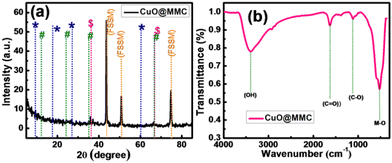 |
| | Fig. 2 Representative (a) XRD spectrum and (b) FTIR spectrum of MXene CuO20@MMC. | |
Fig. 2(b) exhibits the FTIR spectrum of the CuO20@MMC thin film, which shows absorption bands at ∼3435 cm−1 attributed to the surface terminating hydroxyl group due to water adsorbed on the surface and strong hydrogen-bonded –OH. The other stretching vibrations observed include CO at 1631 cm−1 and C–O at 1013 cm−1, which could be attributed to the surface-adsorbed moisture and physical absorption of CO2 while preparing the FTIR samples.34–36 The characteristic absorption bands of cupric oxide (M–O band) appear at 525 cm−1 and are attributed to the tensile vibration of Cu–O.
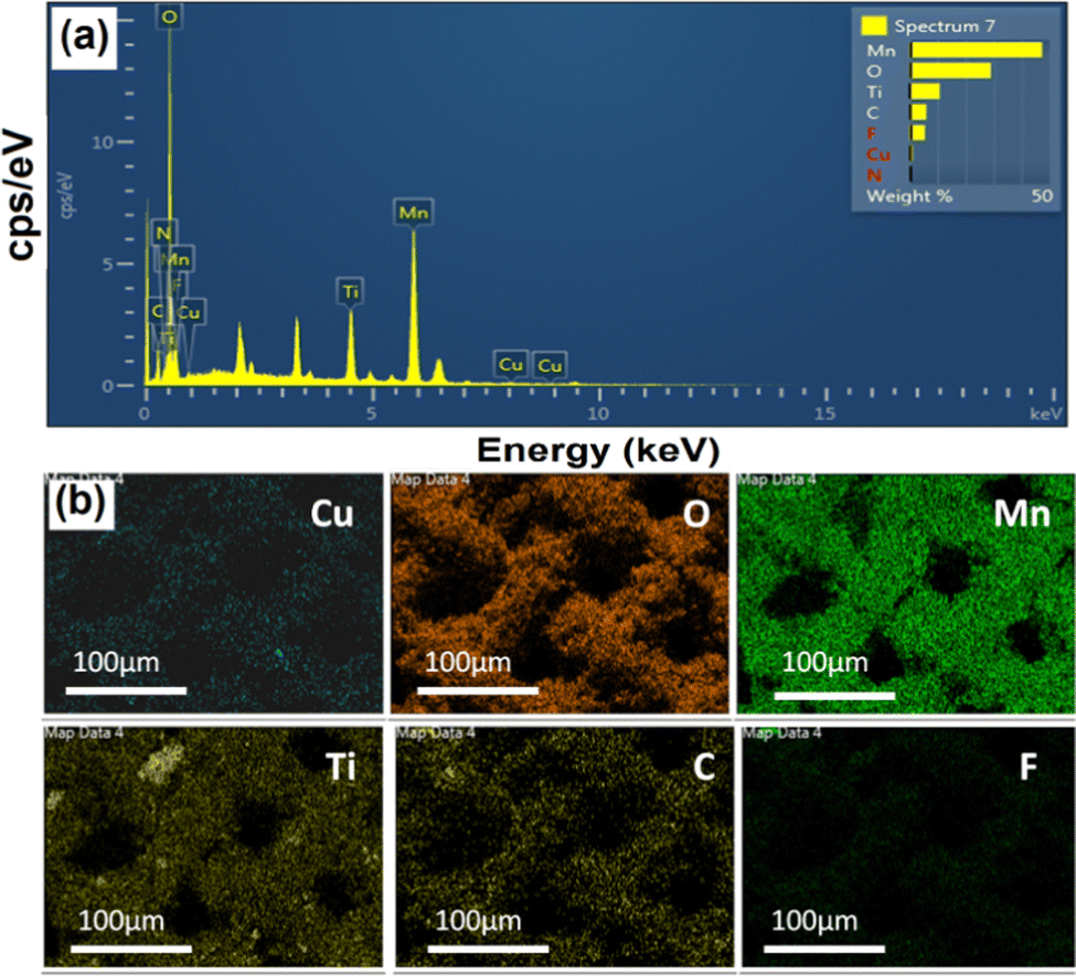
The surface morphology of the synthesized CuO, MnO2, MX, and CuO20@MMC thin films was studied using scanning electron microscopy. Fig. 3(a–d) display high magnification images of CuO, MnO2, MX, and CuO20@MMC thin films exhibiting nano spine, nanograin, nano-sheet, and nanosheet decorated with nanograin morphologies, respectively. Fig. 3(a) shows the nano spine-like morphology of CuO thin films synthesized by the SILAR method. Fig. 3(b) shows the uniform nanograin-like morphology of MnO2 synthesized by R-CBD. Fig. 3(c) shows multilayered nanosheets of MX delaminated with a clear border, smooth surface, and few defects. The average thickness of the MX layers is ∼1.7 μm. Fig. 3(d) shows the nanosheets being decorated with nanograins, which increases the SSA and ultimately enhances the Csp. The morphology of CuO has been suppressed as it was covered by the morphologies of MnO2 and MXene. To further justify the formation of CuO20@MMC composite thin films, EDAX, and elemental mapping were performed. Fig. 4(a) shows the EDS spectrum which displays the elemental chemical composition of CuO20@MMC thin films. The EDS elemental mapping was also performed and the data presented in Fig. 4(b) confirm the presence and uniform distribution of Cu, O, Mn, Ti, C, and F in the CuO20@MMC thin film sample.
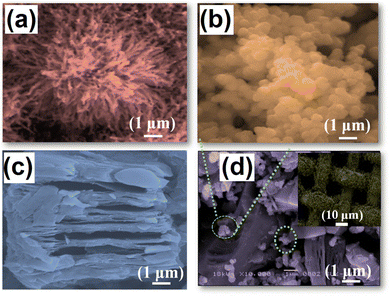 |
| | Fig. 3 Representative high-resolution SEM images of (a) CuO, (b) MnO2, (c) MXene, and (d) CuO20@MMC and the inset show low-resolution images. | |
 |
| | Fig. 4 (a) Representative EDAX spectrum and (b) the elemental (Cu, O, Mn, Ti, C, and F) mapping of the synthesized CuO20@MMC thin film. | |
The surface area of an electrode material is an important metric for supercapacitor applications since it influences the capacitance, impedance, and charge–discharge rate. The electrolyte ion/electron access is made easier by engineering the porosity of the electrode material. Thus, the surface area and pore size distribution of CuO, MX, MnO2, and CuO20@MMC powder samples were determined using the BET adsorption/desorption technique and the BJH method, as shown in Fig. 5. The powder samples were obtained by scratching out the deposited material from the thin film and then subjected to BET analysis. The nitrogen adsorption/desorption curves in Fig. 5(a–d) display a type IV isotherm and H3 hysteresis, respectively, demonstrating the mesoporous nature of CuO, MX, MnO2, and CuO20@MMC. For the samples CuO, MX, MnO2, and CuO20@MMC, these type IV isotherms have comparatively small hysteresis loops that may be apparent at a relative pressure of 0.1 to 1. The BET surface area of CuO, MX, MnO2 and CuO20@MMC is 38.43, 19.5, 37.8, and 78.87 m2 g−1, respectively. The inset images show a pore size distribution of ∼1.48, 1.83, 1.80, and 1.46 nm of CuO, MX, MnO2, and CuO20@MMC, respectively. It is important to note that the interlayer coupling in MXenes and the irreversible stacking phenomenon are the causes of the lowering of the SSA of MX (19.5 m2 g−1). This inevitably takes place during the sample preparation/drying process and the electrode slurry coating process, which prevents the MXene surface and functional groups from being utilized to their full potential. Restacking causes an increase in “buried” area, which fatally reduces the amount of surface area that is available, preventing the electrolyte from penetrating the MXene layers and subsequently restricting the electrochemical performance of the electrode material.37 While an increase in the SSA of CuO20@MMC is noted due to the exfoliation and separation of MXene flakes cumulatively because of ultrasonication, deposition, and penetration of CuO nano spines and MnO2 porous nanograins within the layered architecture. Thus, the metal oxide MnO2 intercalates between the layers of MXene, and hence, the surface area of the ternary composite enhances dramatically when compared to the individual metal oxide. Thus, the higher SSA results in a higher electrochemical performance of the electrode.
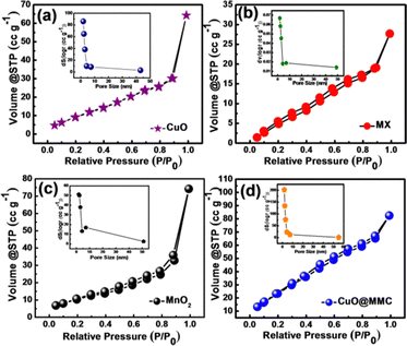 |
| | Fig. 5 N2 adsorption–desorption isotherms and the respective insets showing the BJH pore size distribution of (a) CuO, (b) MX, and (c) MnO2, and (d) CuO20@MMC thin film, respectively. | |
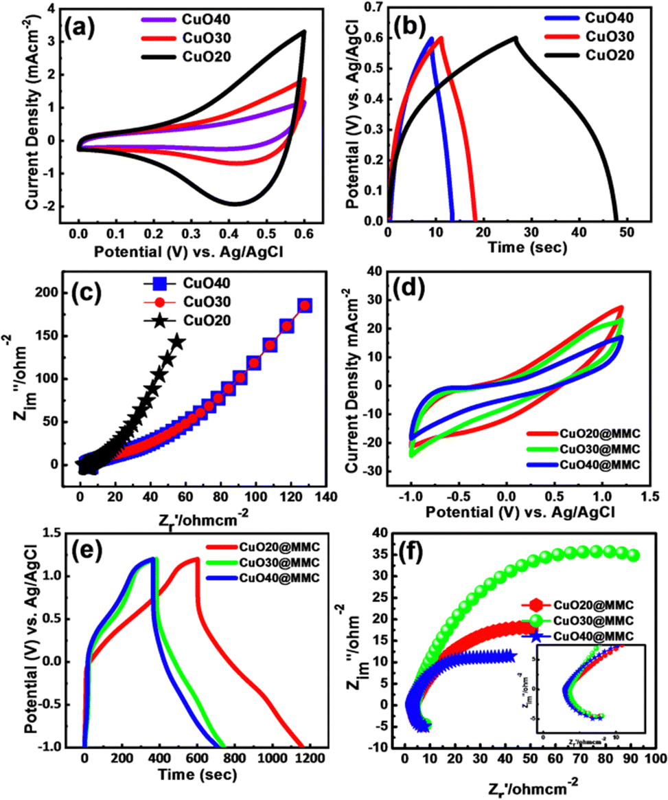
We further evaluated the electrochemical performance of the electrodes using the standard three-electrode system with CuO20@FSSM, CuO30@FSSM, and CuO40@FSSM, as the working electrode in 1 M KOH and CuO20@MMC, CuO30@MMC, and CuO40@MMC as the working electrode in 1 M Na2SO4 aqueous electrolyte. Fig. 6(a) displays the cyclic voltammetry (CV) curves of the CuO20@FSSM, CuO30@FSSM, and CuO40@FSSM films integrated area at the same sweep speed at 100 mV s−1 recorded in 1 M KOH. The area under the curve of the CuO20@FSSM film is larger than that of CuO30@FSSM and CuO40@FSSM. Furthermore, the individual CV curves for CuO20@FSSM, CuO30@FSSM, and CuO40@FSSM films at various scan rates are shown in Fig. S2(a), (a′) and (a′′) (ESI†), respectively, using different scanning rates from 10 to 100 mV s−1 in 1 M KOH. Fig. 6(b) shows comparative GCD curves recorded using CuO20@FSSM, CuO30@FSSM, and CuO40@FSSM films at a current density of 0.9 mA cm−2. The CuO20@FSSM composite implies more time to discharge as compared to pristine CuO30@FSSM and CuO40@FSSM indicating its excellent performance, and confirming that CuO20@FSSM shows higher electrochemical performance.
 |
| | Fig. 6 Comparative (a) CV, (b) GCD, and (c) EIS of CuO20@FSSM, CuO30@FSSM, and CuO40@FSSM films. Comparative (d) CV, (e) GCD, and (f) EIS of CuO20@MMC, CuO30@MMC, and CuO40@MMC thin films, respectively. | |
The calculated Csp of CuO20@FSSM, CuO30@FSSM, and CuO40@FSSM thin films at a current density of 0.9 mA cm−2 is 17.56, 3.21, and 2.56 F g−1, respectively. To investigate the ion transport behaviour and resistance of the sample electrodes, electrochemical impedance spectroscopy (EIS) was conducted and the results are shown in Fig. 6(c). The Nyquist plots are composed of a low-frequency straight line and a smaller semicircle in the high-frequency region. The equivalent series resistance (ESR), which consists of the combined series resistance of the electrolyte, electrode, current collectors, and the electrode/current collector contact resistance, is represented by the intersection of a semicircle's beginning point with the x-axis at higher frequency. Fig. 6(c) shows that the ESR value obtained from the intersection of the Nyquist plot of CuO20@FSSM, CuO30@FSSM, and CuO40@FSSM at the X-axis is 6.0, 6.2, and 6.3 Ω, respectively. The charge transfer resistance (Rct) at the interface between the electrode material and electrolyte is calculated using the diameter of the semicircle in the high-frequency zone. The charge transfer resistance (Rct) value of the CuO20@FSSM, CuO30@FSSM, and CuO40@FSSM thin film obtained from the diameter of the semicircle is 0.5, 0.52, and 0.53 Ω, respectively.
Fig. 6(d) shows the comparative cyclic voltammetry (CV) curves CuO20@MMC, CuO30@MMC, and CuO40@MMC as the working electrode in 1 M Na2SO4 aqueous electrolyte, graphite as the counter electrode and a saturated Ag/AgCl electrode as a reference electrode at RT scanned at 125 mV s−1 in 1 M KOH electrolyte within the potential window of −1 to 1.2 V. The area of the CuO20@MMC CV curves was found to be larger than CuO30@MMC and CuO40@MMC even at a high scan rate of 125 mV s−1 indicating good rate capability, high rate of performance, and reversibility. Fig. 6(e) displays comparative GCD curves of the CuO20@MMC, CuO30@MMC, and CuO40@MMC films at current densities of 10 mA cm−2. The CuO20@MMC composite implies more time to discharge as compared to CuO30@MMC and CuO40@MMC indicating its excellent performance and also confirming that CuO20@FSSM shows higher electrochemical performance. The calculated Csp of the electrodes by using equation 1 and the GCD discharge time are 924.16, 544.54, and 462.54 F g−1, respectively. The individual CV, GCD, and EIS of the synthesized CuO20@MMC, CuO30@MMC, and CuO40@MMC are shown in ESI† Fig. S3. It was observed that the Csp decreases with an increase in current density and is attributed to the insufficient time for the electrolyte ions to complete the electrochemical reaction at a higher current density. Fig. 6(f) displays the Nyquist plots of CuO20@MMC, CuO30@MMC, and CuO40@MMC films. The ESR values obtained from the intersection of the Nyquist plot of CuO20@MMC, CuO30@MMC, and CuO40@MMC at the X-axis are 6.2, 7.2, and 8.1 Ω, respectively. The charge transfer resistance (Rct) values obtained from the diameter of the semicircle are 0.21, 0.33, and 0.43 Ω, for CuO20@MMC, CuO30@MMC, and CuO40@MMC, respectively. The lower ESR and Rct for CuO20@MMC show good electrical conductivity of the electrode, which is attributed to the appropriate MXene contribution to CuO20.
Furthermore, to study the charge storage mechanism of the optimized electrode, the diffusion, and capacitive control processes were investigated by the following Power law,
where
Ip represents the peak current density of the electrode,
a and
b are the adjustable factors, and
v is the scan rate.
Fig. 7(a) shows the CV curves of the CuO20@MMC electrode with varying scan rates.
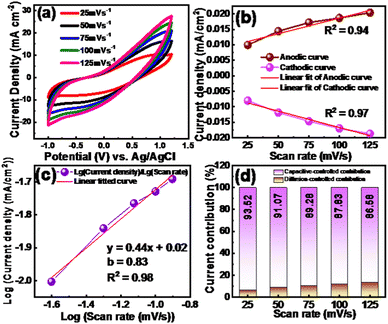 |
| | Fig. 7 (a) CV profiles of CuO20@MMC with varying scan rates, (b) relationship between current density vs scan rate, (c) graph of log(current density) vs. log(scan rate), and (d) contribution ratio of capacities with varying scan rates for the CuO20@MMC. | |
The slope (linear fit) is derived from the scan rate vs current density graph. Fig. 7(b) and (c) derived from the log(scan rate) and log(current density) graph represent the b value. It has been established that the electrode reaction is dominated by diffusion when b = 0.5, and it is dominated by the surface capacitance-controlled process when b = 1. Interestingly, the b value in the case of the CuO20@MMC composite electrode is found to be 0.83, revealing that surface capacitive controlled charge storage is dominant, as shown in Fig. 7(c).
The separate quantification of capacitive controlled and diffusive controlled charge storage is analyzed from the following equation:
where
i is total current,
k1 and
k2 are constants,
k1v is capacitive controlled distribution and
k2v is diffusion controlled distribution.
k1 and
k2 are determined by plotting the (
i/√
v)
versus √
v. The value of
k1 is equivalent to the slope and the value of
k2 is equivalent to the
y-intercept. The distribution of charge storage in CuO20@MMC composite electrodes ranging from 25–125 mV s
−1 is displayed in
Fig. 7(d). The bar diagram presents the contribution of the capacitive (violet) and diffusive (brown) charge storage to the total current. The coexisting violet and brown regions, confirms the contribution of both capacitive and diffusive types in the charge storage mechanisms of the electrode. At the 25 mV s
−1 scan rate, 93.52% contribution was capacitive, and it was found to decrease to 86.58% at 125 mV s
−1.
Fig. 7(d) exemplifies that the capacitive contribution decreases with increasing scan rate. Thus, the electrodes exhibit both types of charge storage with a large amount of charge storage by the capacitive process. This signifies that more contribution of capacitive controlled charge storage takes place due to the presence of MXene EDLC behaviour and only a small amount of CuO and MnO
2 is involved in charge storage due to its pseudo capacitive characteristics. Thus, it can be concluded that the capacitive controlled contribution is dominant at a high scan rate and contributes more to the total capacitance of the CuO20@MMC composite electrode.
By constructing an ASC device with MX serving as a counter electrode in a PVA–KOH gel electrolyte, the practical use of the CuO20@MMC composite electrode was examined. The electrochemical capacitance of the CuO20@MMC//MX solid-state ASC device is determined from the discharge time and total mass of the MMC-4 and MX electrodes according to eqn (1). Moreover, it has been found that the energy density rises as the voltage window widens. The voltage window of 0–1.6 V was selected for the electrochemical tests and evaluation of the CuO20@MMC/MX solid-state ASC device based on the studies mentioned above. Fig. 8(a) demonstrates the unchanged shape of the CV curves of the CuO20@MMC//MX solid-state ASC device at various scan rates (20 mV s−1 to 100 mV s−1) within a potential window of 0 to 1.6 V suggesting good rate capability. Fig. 8(b) represents the GCD plot of the CuO20@MMC//MX solid-state ASC device at various current densities (2–5 mA cm−2). The ASC device exhibits the Csp of 25.0, 19.5, 15.2, and 8.5 F g−1 at current densities 2, 3, 4, and 5 mA cm−2, respectively, calculated from the discharge time of the device. The device exhibits a maximum power density of 571.2 W kg−1 at an energy density of 3.5 W h kg−1. Fig. 8(c) presents the Nyquist plots of the CuO20@MMC//MX asymmetric supercapacitor resulting in Rct of 2.4 Ω and ESR of 3.4 Ω indicating that MXene contributes to the electrical conductivity of the device with the inset showing the fitted equivalent circuit. Fig. 8(d) displays the flexibility of the device in the I, V, and S shape at a scan rate of 100 mV s−1 of the device, which reveals that even with the change in the shape of the device the CV curve shows a slight change demonstrating excellent flexibility. Furthermore, Fig. 9(a) and (b) show the cycling stability of the CuO20@MMC electrode and CuO20@MMC//MX ASC device over 4000 and 2000 cycles, respectively. It is observed that 77.92% of its initial Csp was retained by the electrode even after 4000 continuous GCD cycles at a current density of 10 mA cm−2 exhibiting good cycling stability. While the device exhibited 87.27% of its initial Csp even after 2000 continuous GCD cycles at a current density of 3 mA cm−2 suggesting good durability of the device.
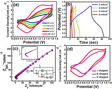 |
| | Fig. 8 Representative (a) CV, (b) GCD and (c) EIS, and (d) the flexibility study of the CuO20@MMC//MX ASC device. | |
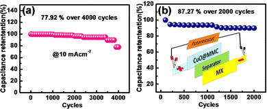 |
| | Fig. 9 (a) Cycling stability of the CuO20@MMC electrode over 4000 cycles and (b) cycling stability of the CuO20@MMC//MX device over 2000 cycles. | |
4. Conclusions
In order to create supercapacitors with high gravimetric capacitances, we propose a straightforward, economical, two-step deposition technique to produce a ternary composite electrode material based on a combination of MXene with metal oxides, specifically MnO2 and CuO. The porous series of CuO@MMC ternary nanocomposites provide abundant channels and access for electrolyte ions, and hence, enhance the electrochemical performance. The comparative study for the supercapacitive performance of CuO@MMC was investigated and further employed in the fabrication of the ASC device. The CuO20@MMC favoured electrochemical performance exhibiting a Csp of 924.16 F g−1 at a current density of 10 mA cm−2 with good cycling retention of 77.92% of its initial Csp in 1 M Na2SO4 electrolyte over 4000 cycles. Furthermore, when employed in a device, the CuO@MMC//MX ASC device exhibits a Csp of 25.0 F g−1 with a maximum power density of 571.2 W kg−1 at an energy density of 3.5 W h kg−1. The device exhibited 87.27% of its initial Csp retained even after 2000 continuous GCD cycles at a current density of 3 mA cm−2 suggesting the device's durability. Our findings suggest that the CuO@MMC electrode is a technically reasonable choice for an energy storage device.
Author contributions
RAC – conceptualization, investigation, methodology, formal analysis, interpretation of the data and writing, DMU – data curation, interpretation of the data, review of the article, ASR – data curation, review of the article, JYC – formal analysis, editing, review of the article, AVG – conceptualization, methodology, formal analysis, interpretation of the data, editing, supervision, and approval of the final version.
Conflicts of interest
The authors declare no conflict of interest.
Acknowledgements
The author RAC gratefully appreciates Chhatrapati Shahu Maharaj Research Training and Human Development Institute (SARTHI), Pune Government of Maharashtra for the financial support in the form of Chhatrapati Shahu Maharaj National Research Fellowship-2019 (CSMNRF-2019). We are thankful to the Department of Chemistry, Shivaji University, Kolhapur for providing the research facilities. We are thankful to Shivaji University Group for Advanced Research “SUGAR” for the helpful discussion.
References
- L. Dai, D. W. Chang, J.-B. Baek and W. Lu, Small, 2012, 8, 1130–1166 CrossRef CAS PubMed.
- Y. Ma, P. Li, J. W. Sedloff, X. Zhang, H. Zhang and J. Liu, ACS Nano, 2015, 9, 1352–1359 CrossRef CAS PubMed.
- D. T. Pham, T. H. Lee, D. H. Luong, F. Yao, A. Ghosh, V. T. Le, T. H. Kim, B. Li, J. Chang and Y. H. Lee, ACS Nano, 2015, 9, 2018–2027 CrossRef CAS PubMed.
- D. Zha, P. Xiong and X. Wang, Electrochim. Acta, 2015, 185, 218–228 CrossRef CAS.
- Y. Huang, Y. Li, Z. Hu, G. Wei, J. Guo and J. Liu, J. Mater. Chem. A, 2013, 1, 9809–9813 RSC.
- B. Mendoza-Sánchez and Y. Gogotsi, Adv. Mater., 2016, 28, 6104–6135 CrossRef PubMed.
- M. Naguib, O. Mashtalir, J. Carle, V. Presser, J. Lu, L. Hultman, Y. Gogotsi and M. W. Barsoum, ACS Nano, 2012, 6, 1322–1331 CrossRef CAS PubMed.
- P. Lian, Y. Dong, Z.-S. Wu, S. Zheng, X. Wang, S. Wang, C. Sun, J. Qin, X. Shi and X. Bao, Nano Energy, 2017, 40, 1–8 CrossRef CAS.
- C. Zhang, B. Anasori, A. Seral-Ascaso, S.-H. Park, N. McEvoy, A. Shmeliov, G. S. Duesberg, J. N. Coleman, Y. Gogotsi and V. Nicolosi, Adv. Mater., 2017, 29, 1702678 CrossRef PubMed.
- M. Ghidiu, M. R. Lukatskaya, M.-Q. Zhao, Y. Gogotsi and M. W. Barsoum, Nature, 2014, 516, 78–81 CrossRef CAS PubMed.
- Z. Lin, D. Barbara, P.-L. Taberna, K. L. Van Aken, B. Anasori, Y. Gogotsi and P. Simon, J. Power Sources, 2016, 326, 575–579 CrossRef CAS.
- H.-z Yang and J.-p Zou, Trans. Nonferrous Met. Soc., 2018, 28, 1808–1818 CrossRef CAS.
- P. Poizot, S. Laruelle, S. Grugeon, L. Dupont and J. Tarascon, Nature, 2000, 407, 496–499 CrossRef CAS PubMed.
- R.-R. Bi, X.-L. Wu, F.-F. Cao, L.-Y. Jiang, Y.-G. Guo and L.-J. Wan, J. Phys. Chem. C, 2010, 114, 2448–2451 CrossRef CAS.
- J. Eskusson, P. Rauwel, J. Nerut and A. Jänes, J. Electrochem. Soc., 2016, 163, A2768–A2775 CrossRef CAS.
- M. Wang, S. Cheng, G. Dang, F. Min, H. Li, Q. Zhang and J. Xie, Int. J. Electrochem. Sci., 2017, 12, 6292–6303 CrossRef CAS.
- A. A. Kashale, Madagonda M. Vadiyar, S. S. Kolekar, B. R. Sathe, J.-Y. Chang, H. N. Dhakal and A. V. Ghule, RSC Adv., 2017, 7, 36886–36894 RSC.
- H. Wang, Q. Ren, D. J. L. Brett, G. He, R. Wang, J. Key and S. Ji, J. Power Sources, 2017, 343, 76–82 CrossRef CAS.
- L. Li, S. Peng, H. B. Wu, L. Yu, S. Madhavi and X. W. Lou, Adv. Energy Mater., 2015, 5, 1500753 CrossRef.
- W. K. Chee, H. N. Lim, I. Harrison, K. F. Chong, Z. Zainal, C. H. Ng and N. M. Huang, Electrochim. Acta, 2015, 157, 88–94 CrossRef CAS.
- R. B. Rakhi, B. Ahmed, M. N. Hedhili, D. H. Anjum and H. N. Alshareef, Chem. Mater., 2015, 27, 5314–5323 CrossRef CAS.
- M. Naguib and Y. Gogotsi, Acc. Chem. Res., 2015, 48, 128–135 CrossRef CAS PubMed.
- R. B. Rakhi, B. Ahmed, M. N. Hedhili, D. H. Anjum and H. N. Alshareef, J. Mater. Chem., 2015, 27, 5314–5323 CrossRef CAS.
- G. P. Kamble, A. S. Rasal, S. B. Gaikwad, V. S. Gurav, J.-Y. Chang, S. S. Kolekar, Y.-C. Ling and A. V. Ghule, ACS Appl. Nano Mater., 2021, 4, 12702–12711 CrossRef CAS.
- J.-W. Wang, Y. Chen and B.-Z. Chen, J. Alloys Compd., 2016, 688, 184–197 CrossRef CAS.
- Z. Su, C. Yang, B. Xie, Z. Lin, Z. Zhang, J. Liu, B. Li, F. Kang and C. P. Wong, Energy Environ. Sci., 2014, 7, 2652–2659 RSC.
- R. B. Rakhi, B. Ahmed, D. Anjum and H. N. Alshareef, ACS Appl. Mater. Interfaces, 2016, 8, 18806–18814 CrossRef CAS PubMed.
- S. Wu, W. Lv, T. Lei, Y. Han, X. Jian, M. Deng, G. Zhu, M. Liu, J. Xiong, J. H. Dickerson and W. He, Adv. Energy Mater., 2017, 7, 1700105 CrossRef.
- H. Fang, Y. Pan, M. Yin and C. Pan, J. Mater. Sci.: Mater. Electron., 2019, 30, 14954–14966 CrossRef CAS.
- C. Zhao, Q. Wang, H. Zhang, S. Passerini and X. Qian, ACS Appl. Mater. Interfaces, 2016, 8, 15661–15667 CrossRef CAS PubMed.
- X. Li, G. Fan and C. Zeng, Int. J. Hydrogen Energy, 2014, 39, 14927–14934 CrossRef CAS.
- X. Xie, S. Chen, W. Ding, Y. Nie and Z. Wei, Chem. Commun., 2013, 49, 10112–10114 RSC.
- Y. X. Zhang, X. D. Hao, F. Li, Z. P. Diao, Z. Y. Guo and J. Li, Ind. Eng. Chem. Res., 2014, 53, 6966–6977 CrossRef CAS.
- E. Lee, A. Vahid Mohammadi, B. C. Prorok, Y. S. Yoon, M. Beidaghi and D.-J. Kim, ACS Appl. Mater. Interfaces, 2017, 9, 37184–37190 CrossRef CAS PubMed.
- Y. Li, Z. Xiaobing, J. Wang, Q. Deng, M. Li, S. Du, Y. Han, J. Lee and Q. Huang, RSC Adv., 2017, 7, 24698–24708 RSC.
- S. Xu, G. Wei, J. Li, Y. Ji, N. Klyui, V. Izotov and W. Han, Chem. Eng. J., 2017, 317 Search PubMed.
- L. Li, N. Zhang, M. Zhang, L. Wu, X. Zhang and Z. Zhang, ACS Sustainable Chem. Eng., 2018, 6, 7442–7450 CrossRef CAS.
|
| This journal is © The Royal Society of Chemistry 2023 |
Click here to see how this site uses Cookies. View our privacy policy here. 
 Open Access Article
 This Open Access Article is licensed under a Creative Commons Attribution-Non Commercial 3.0 Unported Licence
 a,
Desta M.
Ulisso
a,
Akash S.
Rasal
b,
Jia Yaw
Chang
b and
Anil Vithal
Ghule
a,
Desta M.
Ulisso
a,
Akash S.
Rasal
b,
Jia Yaw
Chang
b and
Anil Vithal
Ghule