
 Open Access Article
 This Open Access Article is licensed under a
 Creative Commons Attribution 3.0 Unported Licence
Anisotropic valence band dispersion of 2D molecular crystals of C6-DPA and its charge transport dependence†
Qingqing
Wang
 *a,
Jinpeng
Yang
b,
Mats
Fahlman
a and
Xianjie
Liu
*a
*a,
Jinpeng
Yang
b,
Mats
Fahlman
a and
Xianjie
Liu
*a
aLaboratory of Organic Electronics, Department of Science and Technology, Linkoping University, 60174 Norrkoping, Sweden. E-mail: qingqing.wang@liu.se; xianjie.liu@liu.se
bCollege of Physical Science and Technology, Yangzhou University, Jiangsu 225009, China
First published on 1st April 2023
Abstract
The unique properties and potential optoelectronic applications of two-dimensional molecular crystals (2DMCs) of organic semiconductors make them fascinating research subjects. With advancements in crystal engineering, it is becoming reality to produce 2DMCs with molecular-level thickness and large areas up to the centimeter scale, enabling us to directly explore the electronic structure of 2DMCs and to correlate them with their electrical properties. Here, we investigated the electronic structure of 2DMCs of C6-DPA using photoemission spectroscopy and electrical properties based on organic field-effect transistors. Our findings indicate that anisotropic band dispersion is present in the ab plane of the 2DMCs of C6-DPA which is in good agreement with the in-plane anisotropic mobility, i.e., the direction of the strongest molecular overlap coincides with the direction of the highest mobility.
Introduction
2D molecular crystals (2DMCs) have emerged as promising materials for (opto)electronic applications1–7 owing to their merits of well-ordered molecular packing, low density of impurities and defects, molecular uniform thickness and tailor-made properties. Molecular arrangement within 2DMCs typically exhibits anisotropic packing due to the low symmetry of organic molecules,8,9 leading to anisotropic mobility. Therefore, a thorough comprehension of the anisotropic transport properties10 and the underlying physical origin11 behind anisotropy associated with packing motifs should be well understood for gaining further insight into how molecular packing affects the observed (opto)electronic device performance, ultimately guiding rational molecular design of novel organic semiconductors with desired properties and high-performance device fabrication.Unfortunately, experimental information regarding structure–property relationships is relatively scarce. Structure–property relationships of only a few organic small molecules have been studied, e.g., rubrene12,13 and pentacene.14 The organic field-effect transistors15,16 offer a valuable tool of invertigating anisotropic mobility since their conductive channel is tightly linked to the molecular arrangement at the interface. However, the electronic structure in direct relationship with the charge mobility often lacks accurate characterization. To some extent, this is due to low conductivity of organic semiconductors resulting in sample charging during measurements and difficulty in preparing large-area well-ordered organic single crystals. The emergence of 2DMCs provides a great opportunity to explore the intrinsic electronic structure, because they not only overcome the limitation on the film dimension but also alleviate the sample charging problem.
Anthracene derivatives17,18 have been found to integrate both high luminescence efficiency and carrier mobility, endowing them with great potential to become excellent (opto)electronic materials. One of the anthracene derivatives, C6-DPA, a well-studied p-type organic semiconductor material with a large band gap (3.0 eV) and a deep highest occupied molecular orbital of 5.6 eV determined using HeI ultraviolet photoemission spectroscopy (Fig. S1, ESI†), is more stable under ambient atmosphere than well-known purely hydrocarbon molecules, i.e., rubrene19 and pentacene.20,21 In addition, with its good solubility in common solvents, C6-DPA is often used as an archetype material in 2D crystal fabrication techniques,22–26 producing large area with the thickness even scaling down to the monolayer molecular crystals of C6-DPA. The highest mobility of organic field effect transistors (OFETs) based on the 2DMCs of C6-DPA23 is 4 cm2 V−1 s−1, which is well above that of a-Si. Based on the above advantages, we therefore selected C6-DPA to explore the structure–property relationship.
In this study, based on the previously reported layer-defining strategy method proposed by the Li group,27 we successfully prepared large-area bilayer 2DMCs of C6-DPA. Combined with multiple characterization techniques including polarized optical microscopy (POM), transmission electron microscopy and selected-area electron diffraction (TEM and SAED) and near-edge X-ray absorption fine structure (NEXAFS), high-quality 2DMCs of C6-DPA with an upright orientation were obtained. We then directly determine the valence band characters of 2DMCs of C6-DPA along the surface normal with a tunable photon energy from 40 to 80 eV and probe the in-plane dispersion using angle-resolved ultraviolet photoemission spectroscopy (ARUPS). We found that the anisotropic valence band dispersion exists only in the ab plane and the absence of dispersion along the surface normal. The in-plane dispersion is clearly along the well-packed [010] direction (Γ–B, b axis) and the corresponding effective mass is 3.63m0 with band-like transport properties. The direction along [100] (Γ–Y, a axis) shows no band dispersion. The mobility based on OFETs along the b axis is 0.88 cm2 V−1 s−1, while 0.43 cm2 V−1 s−1 along the a axis, leading to an anisotropic charge transport ratio of 2 in the ab plane. A consistency between band dispersion and the highest mobility is observed. It should be noted that the problem of “sample charging” during ARUPS measurements is avoided due to the high quality of 2DMCs with ultralow density of trap states. The band structure is thus obtained directly without laser illumination.
Experimental section
C6-DPA 2DMC growth
For solution preparation, C6-DPA was dissolved in chlorobenzene with a concentration of 0.5 mg ml−1. Then, the solution was treated by ultrasound for half an hour and then purified using a 0.2 μm filter. The weighing bottles (60 mm × 30 mm) were cleaned using acetone, isopropyl alcohol and deionized water (DI) successively. After drying, 25 ml of glycerol was added into each weighing bottle as a liquid substrate. A droplet of the C6-DPA solution was drop-cast onto the glycerol surface and then sealed with a lid for crystal growth. After the solvent was completely evaporated, floating C6-DPA 2DMCs on glycerol surface were produced.Characterization of materials
Prior to characterization, 2DMCs were annealed in a vacuum oven at 120° for 2 hours to remove water and other residues. Cross-polarized optical microscopy images were taken using an Olympus MX50 inspection microscope. Atomic force microscopy (AFM) was performed using a Bruker Veeco Dimension 3100 microscope. Bright-field transmission electron microscopy and selected-area electron diffraction measurements were conducted using a Tecnai G2 F20 S-TWIN transmission electron microscope, where samples were transferred onto a Cu grid. Ultraviolet photoelectron spectroscopy (UPS) was carried out using an Scienta ESCA 200 microscope with a non-monochromatized HeI source (21.2 eV). Near-edge X-ray absorption fine structure measurements were carried out at the FlexPES beamline (photon energy 40–1500 eV) of the MAX IV laboratory, Lund, Sweden. The electrical measurements of the devices are conducted using a semiconductor parameter analyzer (Keithley 4200 SCS) on a probe station.Valence band measurement
Photon energy dependent angle-resolved UPS (ARUPS) was carried out at the MatLine beamline at ASTRID2 at the Department of Physics and Astronomy, Aarhus University. The beamline is equipped using a Scienta electron energy analyzer and an SX-700 monochromator.The photoelectron-emission-angle-dependent ARUPS measurements were performed using a high-sensitivity apparatus with an MBS A-1 hemispherical electron energy analyzer and a monochromatic He Iα (hν = 21.22 eV) radiation source, where the total energy resolution was set to be 30 meV. The angle-resolving mode of the analyzer was at an acceptance angle of ±18° at an angular resolution of ∼0.34° without changing the angular position of the analyzer against the surface normal.
Device fabrication
Prior to the transfer of 2DMCs to the solid substrates, SiO2/Si substrates are successively cleaned using de-ionized water, Piranha solution (70/30 vol./vol. H2SO4/H2O2), de-ionized water, acetone and isopropanol, then treated with oxygen plasma at 50 W for 15 min, and finally modified them with OTS using a vapor phase method. Then the top-contacted bottom-gated structure is adopted by stamping Au (120 nm) stripes on the 2DMCs of C6-DPA as the source and drain electrodes.Theoretical methods
Density functional theory (DFT) calculations were performed using the Perdew–Burke–Ernzerhof (PBE) generalized gradient approximation (GGA) in the Vienna Ab Initio Simulation Package (VASP) to extract the band structure and DOS of the 2D crystals of C6-DPA. Calculations were performed with a plane-wave cutoff of 520 eV on a 15 × 15 × 1 Monkhorst–Pack k-point mesh. For structural relaxation, all atoms are allowed to relax until atomic forces become smaller than 0.01 eV Å−1.Results and discussion
The facile preparation of layer-controllable C6-DPA 2DMCs is achieved by depositing a chlorobenzene solution of C6-DPA onto a glycerol substrate. The chosen glycerol substrate, which has both high viscosity and high surface tension, offers several advantages over other liquid substrates such as water. The high surface tension28 (g = 63.1 mN m−1 at 21 °C) leads to the maximum spreading of the casting solution, extending the range of the available low surface tension solvents. Meanwhile, the high viscosity29 (1412 cP at 20 °C) ensures that the solution is fixed on the surface of the liquid substrate, avoiding the problem of the dynamic movement of the liquid substrate that occurs with low viscosity liquid substrates. The suppressed coffee-ring effect and minimized nucleation density thus facilitate the growth of the centimeter-sized bilayer 2DMCs of C6-DPA after solvent evaporation.The as-grown 2DMCs can be easily transferred to various substrates for characterization, such as transparent substrates, support grids, and conductive substrates. After diluting the glycerol substrate with water, the substrate can be dipped into water at a small angle to fish out the 2DMCs. The 2DMCs of C6-DPA were transferred to a glass substrate to characterize their quality. Under POM, the 2DMCs exhibit a uniform color, a sharp edge, and no obvious cracks (Fig. 1a), indicating the high quality of the obtained 2DMCs, further evidenced by the XRD data with both straight baseline and sharp peaks (Fig. S2, ESI†). When the sample is rotated 45°, the color of the whole film changes uniformly from light to dark (Fig. 1b), a typical feature of the single-crystalline nature. The AFM measurement revealed a thickness of 5.98 nm of the sample transferred to the gold substrate (Fig. 1c), suggesting the bilayer 2DMCs of C6-DPA. Bright-field transmission electron microscopy (TEM) and selected-area electron diffraction (SAED) performed on a copper grid provide further evidence for the highly ordered structure of 2DMCs. As evident from Fig. 1d, the obtained 2DMCs show a uniform morphology over the whole selected area in which the SAED pattern exhibits a clear and ordered set of diffraction spots (inset in Fig. 1d), indicating that the whole film is a single crystal.
 | ||
| Fig. 1 Characterization of the 2DMCs of C6-DPA. (a and b) Cross-polarized optical micrographs. The uniform color change over the whole micrograph indicates that the 2DMCs under a field of view are single crystals. (c) AFM image of 2DMCs on a gold substrate with a thickness of 5.98 nm, corresponding to the bilayer 2DMCs. (d) TEM image and the corresponding SAED patterns. (e) Carbon K-edge angle-resolved NEXAFS spectra. (f) The fitted dichroic ratio R by fitting the experimental peak intensity of π* as a function of the square sine of an incident angle (θ) and a corresponding title angle (a) of the conjugated plane. | ||
We finally utilized angle-dependent NEXAFS to assess the preferred molecular orientation in the 2DMCs of C6-DPA transferred on the gold substrate by measuring the absorption of polarized X-rays at different angles with respect to the surface normal, which is sensitive to the molecular orientation to the electric vector of the X-rays.30 For the purely hydrocarbon molecule of C6-DPA, the carbon K-edge NEXAFS spectrum corresponds to resonance transition from the carbon 1s (C 1s) orbital to π* antibonding orbitals, where the orientation of the transition dipole moment is perpendicular to the ring plane. By the measurement of the absorption intensity of X-rays via partial yield mode under ultrahigh vacuum, we found that the intensity of C 1s → π* resonance transition exhibits strong angular dependence (Fig. 1e), implying highly ordered molecular packing inside the 2DMCs. To quantify the conjugated plane orientation, a dichroic ratio31 (R) was induced. The R value varies from 0.7 to −1 with the molecular orientation varying from the edge-on to the face-on. The derived R value from the C K-edge spectra is presented in Fig. 1f. The conjugated plane of C6-DPA shows the edge-on orientation with R = 0.56, corresponding to a tilted angle of α = 74.53°. This preferred molecular packing within 2DMCs facilitates charge transport in the ab plane along the well-stacked direction and the molecular packing within an active layer is shown in Fig. S3 (ESI†). It should be noted that the obtained values are used to assess the average of a distribution of molecular title angles and these values are far from the “magic” angle that typically is taken to indicate an amorphous sample with the completely random orientation.
Fig. 2 shows the valence band feature of the 2DMCs of C6-DPA recorded under normal emission while increasing the photon energy from 40 eV to 80 eV. To avoid beam damage, every spectrum corresponds to a fresh spot. For the spectrum recorded at 40 eV (bottom line in Fig. 2a), three obvious peaks can be observed in the valence band regime. The binding energy (BE) peaks for these features named Ha, Hb, and Hc are located at 1.5 eV, 2.6 eV, and 3.6 eV, respectively. When the photon energy is increased from 40 eV to 80 eV, the line shape does not exhibit an obvious change, nor does the binding energy of the valence band features (Fig. 2b). The obtained result supports the conclusion of no band dispersion in the normal (kz) direction. From the molecular structure and orientation perspective, the long-terminated alkyl chain and stand-up orientation of C6-DPA molecules in 2DMCs hinder the electronic coupling in the surface normal direction, resulting in negligible band dispersion along the Γ–z (kz) direction.
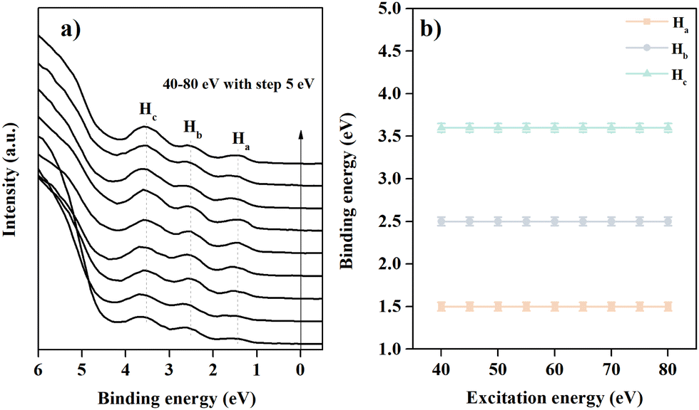 | ||
| Fig. 2 (a) In-depth photoemission spectra of the 2DMCs of C6-DPA measured under normal emission with a tuneable photon energy from 40 eV to 80 eV with a step of 5 eV. (b) The evolution of the binding energy of the three features as a function of excitation energy. | ||
We then probe the in-plane band dispersion using ARUPS. The molecular axes in the ab plane are orthogonal, confirmed using the SAED pattern. The ARUPS spectra were taken along these two directions (Γ–B and Γ–Y) and are plotted on the E–k‖ plane in Fig. 3 where the vertical and horizontal axes represent the binding energy (E) and the surface parallel component of the electron wavenumber (k‖). The ARUPS data present here are in the BE region of 0.1 to −2 eV, corresponding to feature Ha. The theoretical HOMO band is overlaid on the experimental data (yellow dots). The experimentally obtained E–k‖ relationship of Ha feature agrees fairly well with the band calculation. From Fig. 3a, one can clearly observe an energy dispersion of the HOMO band, whereas deeper lying bands do not exhibit an apparent dispersion. No significant band dispersion is observed in the Γ–Y direction, neither in the HOMO nor in deeper lying bands (Fig. 3b). The evolution of all features in the valence band region is shown in Fig. S4 (ESI†). All results corroborate that the valence band maximum (VBM) is located at the Γ point.
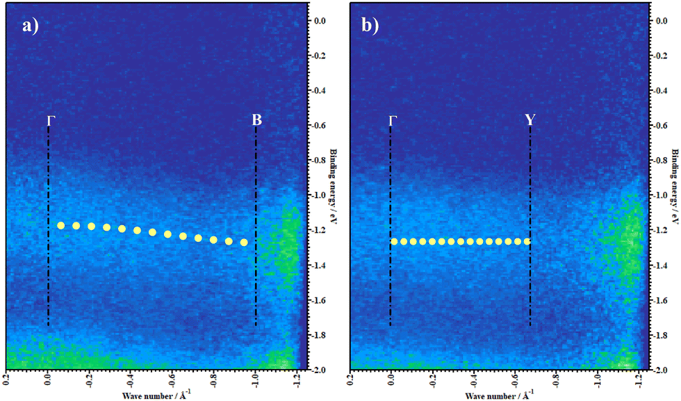 | ||
| Fig. 3 ARUPS E–k‖ mapping of the 2DMCs of C6-DPA along the (a) Γ–B and (b) Γ–Y directions. The binding energy is aligned to the Fermi level. k‖ is the surface parallel component of the wavenumber. The theoretically predicted band dispersion behaviour along these two directions is mapped as continuous yellow dots. | ||
Under the one-dimensional tight-binding (1D-TB) approximation, the E–k dispersion along the Γ–B direction20 can be expressed by as E(κ) = Ec + 2t![[thin space (1/6-em)]](https://www.rsc.org/images/entities/i_char_2009.gif) cos(bk‖), where Ec, t, and b represent the energy of the band center, transfer integral and lattice constant of the corresponding crystal axis, respectively. The estimated t from the least-squares fitting with the cosine curve is −0.51 eV for the theoretical predication and −0.026 eV for the present experimental result. For typical p-type OSCs, the hole effective mass (
cos(bk‖), where Ec, t, and b represent the energy of the band center, transfer integral and lattice constant of the corresponding crystal axis, respectively. The estimated t from the least-squares fitting with the cosine curve is −0.51 eV for the theoretical predication and −0.026 eV for the present experimental result. For typical p-type OSCs, the hole effective mass (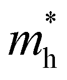 ) at the HOMO band is given by
 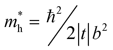 in the vicinity of the Γ point. Our estimation gives
 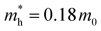 (m0: the free electron mass) and
  for theoretical and experimental results, respectively.
We then discuss whether the charge carrier transport mechanism in the 2DMCs of C6-DPA is band-like or hopping transport. The prerequisite32 for the band-like transport of |4t| > kBT (kB: Boltzmann constant; T: temperature) is fulfilled at room temperature in the present case. From the energy–time uncertainty relationship, the lowest limit of hole mobility can be given by  as
as 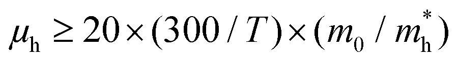 . Therefore, the lowest limit of μh is 5.6 cm2 V−1 s−1, which is comparable with the reported largest μh (4 cm2 V−1 s−1) of OFET based 2D crystals of C6-DPA, suggesting that the hole mobility in the 2D framework is dominated by band-like transport.
To further illustrate the consistency of the light effective mass and high mobility, the charge transport anisotropy of the 2DMCs of C6-DPA was measured at room temperature by fabricating OFETs with a bottom-gate/top-contact (BGTC) configuration (see Fig. 4a), where the nondestructive gold electrodes were transferred on the surface of 2DMCs as the source and drain electrodes, guaranteeing minimum injection barrier and destruction.33 The mobility is extracted from the saturated transfer region by the equation of IDS = (W/2L)μCi(VGS − Vth)2, where IDS is the source–drain current, μ is the field effect mobility, Vth is the threshold voltage, VGS is the applied gate voltage, W/L is the ratio of channel width and length, and the Ci is the specific capacitance (30 nF cm−2). All measurements are conducted under ambient atmosphere and room temperature. Prior to the transfer of the electrodes, the molecular axis in the ab plane is confirmed by polarized microscopy, as shown in Fig. S5 (ESI†). Typically, the lowest mobility is obtained along the a axis ([100] direction), while the highest mobility is obtained from the b axis ([010] direction). These directions show 90° orientation in the ab plane.34
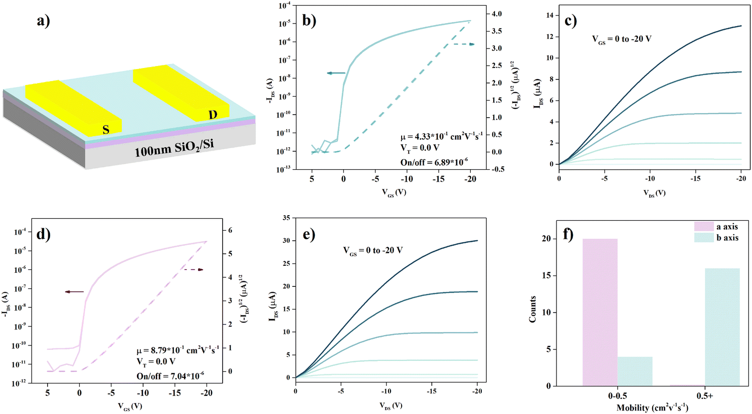 | ||
| Fig. 4 (a) Device schematic of 2DMC based OFETs with the BGTC structure. (b) Typical transfer curve and (c) output curve in the saturation regime along the a axis. The different gate voltages used are, from bottom to top, 0 V, −4 V, −8 V, −12V, −16 V, and −20 V. (d) Transfer curve and (e) output curve in the saturation regime along the b axis. The gate voltage changes from 0 to −20 V in −4 V step from bottom to top. (f) The mobility distribution of 20 devices obtained along these orthorhombic directions. | ||
The transfer curves for such a configuration along the a or b axis directions both exhibit typical p-type characteristics with a well-defined linear and saturation region (Fig. 4b and d). The highest saturation hole mobility obtained along the a axis is 0.43 cm2 V−1 s−1. Meanwhile, the highest mobility obtained along the b axis is 0.88 cm2 V−1 s−1 which leads to a mobility anisotropy of 2 in the ab plane. Tens of measured devices show that the anisotropic mobility is in the range of 2–3. The distribution of mobility (Fig. 4f) along two directions further evidences the anisotropy. It should be noted that there may exist a slight misalignment between the molecular axes and electrodes during device preparation. The corresponding output curves along these two directions are displayed in Fig. 4c and d. The almost linear characteristics of the output curve with a bias in the range of 0 to −3 V (Fig. S6, ESI†) indicate the good contact between electrodes and the sublayer 2DMCs of C6-DPA. Moreover, there is no noticeable hysteresis and bias stress effect in these devices (Fig. S7, ESI†), indicating the negligible charge trap density at the interface between the 2DMCs and the gate dielectric.
The difference of hole mobility between the experimental mobility (0.88 cm2 V−1 s−1) and the calculated mobility from the theoretical band structure (111.8 cm2 V−1 s−1) and the experimental band structure (5.6 cm2 V−1 s−1) can be clearly seen. The disagreement can be partly attributed to impurities and defects leading to the enhanced carrier–phonon scattering, thus increasing the effective mass in real crystals.35 The relatively low mobility obtained based on OFET devices is the result of a complex interplay between multiple factors.36 One such factor is the presence of inevitable defects during the device fabrication process, while another is the contact resistance typically caused by morphological defects. These defects can act as scattering centers, thereby reducing mobility.
Conclusions
In summary, we produced high-quality 2DMCs of C6-DPA with an upright orientation using the layer-controlled growth strategy. We then used them to explore the room temperature electronic structure using photon-energy dependent UPS and ARUPS and to measure the charge carrier mobility based on OFETs. We found an anisotropic band dispersion in the ab plane, and the absence of vertical dispersion. The obvious band dispersion is along the Γ–B direction, which is in good agreement with the theoretical band structure. The effective mass was evaluated to be 3.63 m0 along the Γ–B direction under the 1D-TB assumption, and is larger than the theoretical result (0.18 m0). The corresponding lowest mobility limit is 5.6 cm2 V−1 s−1 for the experimental value, suggesting a band-like transport mechanism. The fabricated OFETs based on C6-DPA exhibit an anisotropy ratio of 2 where the highest mobility is obtained along the b axis, in agreement with the in-plane anisotropic band structure. Overall, this study provides insight into the electronic properties and charge carrier mobility of the 2DMCs of C6-DPA, which can be useful for the development of electronic devices based on these materials.Author contributions
Q. W. contributed to the sample preparation, characterization, device fabrication and measurement, and data analysis; J. Y. carried out the ARUPS measurement and band structure calculation. All the authors participated in the discussion of results and refined this article.Conflicts of interest
There are on conflicts to declare.Acknowledgements
The authors thank financial support from the Swedish Research Council (project grants no. 2016-05498, 2016-05990, 2018-06048, 2020-04538, and 2022-04818), the Swedish Government Strategic Research Area in Materials Science on Functional Materials at Linköping University (Faculty Grant SFO Mat LiU no. 2009 00971), and the Swedish Foundation for Strategic Research (ITM17-0432).Notes and references
- J. Qian, S. Jiang, S. Li, X. Wang, Y. Shi and Y. Li, Adv. Mater. Technol., 2018, 4, 1800182 CrossRef.
- F. Yang, S. Cheng, X. Zhang, X. Ren, R. Li, H. Dong and W. Hu, Adv. Mater., 2018, 30, 1702415 CrossRef PubMed.
- W. Hu and H. Jiang, Angew. Chem., Int. Ed., 2020, 59, 1408–1428 CrossRef PubMed.
- X. Tian, J. Yao, L. Zhang, B. Han, J. Shi, J. Su, J. Liu, C. Li, X. Liu, T. Zhai, L. Jiang, F. Yang, X. Zhang, Y. Zou, R. Li and W. Hu, Nano Res., 2021, 15, 2667–2673 CrossRef.
- L. Zhang, X. Tian, J. Yao, X. Song, S. Yang, S. Guo, Y. Wang, B. Li, X. Ren, Y. Sun, F. Yang, R. Li and W. Hu, J. Mater. Chem. C, 2021, 9, 8834–8841 RSC.
- Y. Wu, Z. Yin, J. Xiao, Y. Liu, F. Wei, K. J. Tan, C. Kloc, L. Huang, Q. Yan, F. Hu and Q. Zhang, ACS Appl. Mater. Interfaces, 2012, 4, 1883–1886 CrossRef CAS PubMed.
- H. Ye, G. Liu, S. Liu, D. Casanova, X. Ye, X. Tao, Q. Zhang and Q. Xiong, Angew. Chem., Int. Ed., 2018, 57, 1928–1932 CrossRef CAS PubMed.
- C. Wang, H. Dong, L. Jiang and W. Hu, Chem. Soc. Rev., 2018, 47, 422–500 RSC.
- C. Reese and Z. Bao, Mater. Today, 2007, 10, 20–27 CrossRef CAS.
- S. C. B. Mannsfeld, J. Locklin, C. Reese, M. E. Roberts, A. J. Lovinger and Z. Bao, Adv. Funct. Mater., 2007, 17, 1617–1622 CrossRef CAS.
- N. Ueno and S. Kera, Prog. Surf. Sci., 2008, 83, 490–557 CrossRef CAS.
- M.-M. Ling, C. Reese, A. L. Briseno and Z. Bao, Synth. Met., 2007, 157, 257–260 CrossRef CAS.
- V. C. Sundar, J. Zaumseil, V. Podzorov, E. Menard, R. L. Willett, T. Someya, M. E. Gershenson and J. A. Rogers, Science, 2004, 303, 1644–1646 CrossRef CAS PubMed.
- Y. Lee, S. Roth and W. Park, Appl. Phys. Lett., 2006, 88, 252106 CrossRef.
- B. Fraboni, R. DiPietro, A. Castaldini, A. Cavallini, A. Fraleoni-Morgera, L. Setti, I. Mencarelli and C. Femoni, Org. Electron., 2008, 9, 974–978 CrossRef CAS.
- Y. Yao, H. Dong, F. Liu, T. P. Russell and W. Hu, Adv. Mater., 2017, 29, 1701251 CrossRef PubMed.
- M. Liu, Y. Wei, Q. Ou, P. Yu, G. Wang, Y. Duan, H. Geng, Q. Peng, Z. Shuai and Y. Liao, J. Phys. Chem. Lett., 2021, 12, 938–946 CrossRef CAS PubMed.
- J. Liu, H. Zhang, H. Dong, L. Meng, L. Jiang, L. Jiang, Y. Wang, J. Yu, Y. Sun, W. Hu and A. J. Heeger, Nat. Commun., 2015, 6, 10032 CrossRef CAS PubMed.
- A. Li, X. Wei, Y. He, C. He, M. U. Ali, H. Yang, O. Goto and H. Meng, Appl. Phys. Lett., 2018, 113, 103301 CrossRef.
- Y. Nakayama, M. Hikasa, N. Moriya, M. Meissner, T. Yamaguchi, K. Yoshida, M. Murata, K. Mase, T. Ueba and S. Kera, J. Mater. Res., 2018, 33, 3362–3370 CrossRef CAS.
- J. E. Anthony, D. L. Eaton and S. R. Parkin, Org. Lett., 2002, 4, 15–18 CrossRef CAS PubMed.
- Z. Chen, S. Duan, X. Zhang and W. Hu, Sci. China: Chem., 2021, 64, 1057–1062 CrossRef CAS.
- C. Xu, P. He, J. Liu, A. Cui, H. Dong, Y. Zhen, W. Chen and W. Hu, Angew. Chem., Int. Ed., 2016, 55, 9519–9523 CrossRef CAS PubMed.
- B. Fu, C. Wang, Y. Sun, J. Yao, Y. Wang, F. Ge, F. Yang, Z. Liu, Y. Dang, X. Zhang, X. Shao, R. Li and W. Hu, Adv. Mater., 2019, 31, 1901437 CrossRef PubMed.
- J. Liu, Y. Yu, J. Liu, T. Li, C. Li, J. Zhang, W. Hu, Y. Liu and L. Jiang, Adv. Mater., 2022, 34, 2107574 CrossRef CAS PubMed.
- X. Tian, J. Yao, S. Guo, Z. Wang, Y. Xiao, H. Zhang, Y. Feng, W. Feng, J. Jie, F. Yang, R. Li and W. Hu, J. Mater. Chem. C, 2022, 10, 2575–2580 RSC.
- W. Hu, J. Y. Yao, Y. Z. Zhang, X. T. Tian, X. Z. Zhang, H. Z. Zhao, X. Z. Zhang, J. J. Jie, X. W. Wang and R. L. Li, Angew. Chem., Int. Ed., 2019, 58, 16082–16086 CrossRef PubMed.
- A. S. Alkindi, Y. M. Al-Wahaibi and A. H. Muggeridge, J. Chem. Eng. Data, 2008, 53, 2793–2796 CrossRef CAS.
- J. B. Segur and H. E. Oberstar, J. Ind. Eng. Chem., 1951, 43, 2117–2120 CrossRef CAS.
- T. Schuettfort, L. Thomsen and C. R. McNeill, J. Am. Chem. Soc., 2013, 135, 1092–1101 CrossRef CAS PubMed.
- D. M. DeLongchamp, R. J. Kline, E. K. Lin, D. A. Fischer, L. J. Richter, L. A. Lucas, M. Heeney, I. McCulloch and J. E. Northrup, Adv. Mater., 2007, 19, 833–837 CrossRef CAS.
- Y. Nakayama, Y. Mizuno, M. Hikasa, M. Yamamoto, M. Matsunami, S. Ideta, K. Tanaka, H. Ishii and N. Ueno, J. Phys. Chem. Lett., 2017, 8, 1259–1264 CrossRef CAS PubMed.
- P. Boyu, C. Ke, L. Albert Ho Yuen, C. Ming, L. Yang and K. L. C. Paddy, Adv. Mater., 2020, 32, 2002281 CrossRef PubMed.
- X. Zhao, J. Liu, J. Liu, H. Li, J. Zhang, C. Li, Y. Dong, X. Shi, Y. Sun, J. Liu, M. Lei and L. Jiang, J. Mater. Chem. C, 2022, 10, 10799–10804 RSC.
- M. A. Stoeckel, Y. Olivier, M. Gobbi, D. Dudenko, V. Lemaur, M. Zbiri, A. A. Y. Guilbert, G. D'Avino, F. Liscio, A. Migliori, L. Ortolani, N. Demitri, X. Jin, Y. G. Jeong, A. Liscio, M. V. Nardi, L. Pasquali, L. Razzari, D. Beljonne, P. Samori and E. Orgiu, Adv. Mater., 2021, 33, e2007870 CrossRef PubMed.
- H. Li, N. Tessler and J.-L. Brédas, Adv. Funct. Mater., 2018, 28, 1803096 CrossRef.
Footnote |
| † Electronic supplementary information (ESI) available. See DOI: https://doi.org/10.1039/d3ma00127j |
| This journal is © The Royal Society of Chemistry 2023 |