
 Open Access Article
 This Open Access Article is licensed under a Creative Commons Attribution-Non Commercial 3.0 Unported Licence
3D printing aqueous Ti3C2Tx inks for MXene-based energy devices†
Mofetoluwa
Fagade‡
 a,
Dhanush
Patil‡
b,
Sri Vaishnavi
Thummalapalli
b,
Sayli
Jambhulkar
b,
Dharneedar
Ravichandran
b,
Arunachala M.
Kannan
c and
Kenan
Song
*d
a,
Dhanush
Patil‡
b,
Sri Vaishnavi
Thummalapalli
b,
Sayli
Jambhulkar
b,
Dharneedar
Ravichandran
b,
Arunachala M.
Kannan
c and
Kenan
Song
*d
aMechanical Engineering, School for Engineering of Matter, Transport and Energy (SEMTE), Tempe, AZ 85281, USA
bSystems Engineering, The School of Manufacturing Systems and Networks (MSN), Ira A. Fulton Schools of Engineering, Arizona State University (ASU), Mesa, AZ 85212, USA
cThe Fuel Cell Laboratory, The Polytechnic School, Ira A. Fulton Schools of Engineering, Arizona State University, Mesa, AZ 85212, USA
dAssociate Professor of Mechanical Engineering at University of Georgia (JGA) and adjunct professor of Manufacturing Engineering, The School of Manufacturing Systems and Networks (MSN), Ira A. Fulton Schools of Engineering, Arizona State University (ASU), Mesa, AZ 85212, USA. E-mail: kenan.song@uga.edu
First published on 27th July 2023
Abstract
The miniaturization of microenvironments and increasing demands on modern-day electronics have reinvigorated the search for new candidates to meet these needs. The MXene (Mn+1XnTx) family has been seen as the next major player in the field of microelectronics due to the unique combination of superior properties. Incorporating microelectronics in micropatterned structures via simple, cost-efficient processing also increases the possibilities of using them in smart devices and microsystems. This short communication reports the nanoparticle synthesis, suspension processing, and 3D printing of a titanium carbide (Ti3AlC2)-based MXene, with the derivation from its elemental powders. More importantly, the in situ etching method was employed to create a multi-layered MXene (Ti3C2Tx), showing high efficiency in generating delaminated Ti3C2Tx nanosheets. Afterward, water-based Ti3C2Tx inks were examined in varying (i.e., 30 mg mL−1, 50 mg mL−1, 100 mg mL−1, and 200 mg mL−1) concentrations for optimized rheologies. An ink-writing-based 3D printing method was then used for micropatterning MXene thin-layers on glass or polymer-coated substrates, demonstrating anisotropic electrical properties over varying strain and energy storage capabilities and showing enormous potential for 3D printable devices.
The modern-day transformation as the world has moved into the digital age has brought new concepts to the fold, with the Internet-of-Things foremost among them.1 The ability to relay information seamlessly across objects in a single network has spurred an interest in flexible, wearable, or implantable electronics. These electronic devices include conductors, sensors, actuators, supercapacitors, fuel cells, batteries, and data-storage devices.2–4 As manufacturing technology advances, modern fabrication techniques have been employed due to increasing efficiency and scalability.5 For instance, the printing of electronics has become more influential in processing these products due to the retaining of material properties, the reduction of defects with enhanced printing resolutions, and the improved variety of fabricated architectures, which have a direct consequence on device performances.5–7 These printing methods include conventional (e.g., roll-to-roll, screen, evaporation, microcontact, nanoimprint lithography) and novel 3D printing (e.g., inkjet, aerosol jet, direct ink writing (DIW)).8–12 The DIW is known for its platform modularity, rapid prototyping capability, low cost, and friendly compatibility with a broad range of feedstocks.13
Nanoparticle synthesis and ink formulations are integral in determining the functionality of printable devices or systems. Critical parameters, such as precursors, solvents, and additives, have led to attempts to produce functionalized inks with specialized properties.5,14 Examples have been demonstrated in two-dimensional (2D) materials, such as graphene and black phosphorus, being explored for their potential as nano-additives in different printing inks.14–16 However, the hydrophobic nature of these particles requires additional fine-tuning (e.g., surface functionalization) to achieve desired dispersion stability, rheological processability, and functional properties, which have motivated the search for candidates that can be utilized without complex preparation or property sacrifices.14 A relatively new family of two-dimensional (2D) MXene nanoparticles (NPs), based on metal carbides, nitrides, and carbonitrides, have been deemed suitable for this purpose.17,18 The unique combination of properties, such as hydrophilic behavior resulting from surface terminations while retaining excellent electrical conductivity due to the fast mobility of charge carriers, makes MXenes an ideal additive for conductive inks.14,17,19 During synthesis, MXenes are typically produced by selectively etching the intermediate layers of a layered tertiary carbide or nitride precursor (more commonly referred to as MAX phase).17–21 They follow a general chemical format of Mn+1XnTx (where n = 1–3). M represents an early transition metal (e.g., Ti, V, Cr), X is a carbon or nitrogen element, and Tx represents surface termination groups (e.g., –OH, –F).17–21
This report briefly explores the synthesis of MAX phase precursors from their elemental powders using pressureless-sintering (PS)20 methods (see ESI,† Fig. S1). This study presents a notable advancement in line with our prior publications,22,23 which focused on utilizing templates and patterned substrates to fabricate functional electronic devices using MXene NPs. Herein, we demonstrate the facile fabrication of template-free MXene-based electronics without using additive or rheology modifiers.24,25Fig. 1a illustrates the synthesis mechanism of MXene (i.e., the ternary compound precursors of Ti3AlC2 MAX phase and its etched phase of MXene), the ink formulation, and the 3D printing procedures. More importantly, the exfoliation process used to form the accordion-like structure in multi-layered Ti3C2Tx (Fig. 1a3 and a4) and desquamated 2D flakes (Fig. 1a5 and a6) were from the in situ etching instead of using toxic/evaporative HF (see ESI,† Fig. S2–S4). This significantly improved experimental safety and environmental friendliness. In addition, the methodologies leveraged to manufacture the ink suspensions were based on DI water, showing a high degree of green chemistry and manufacturing sustainability (Fig. 1b, see ESI† for details). DIW-based 3D printing was subsequently used to deposit the aqueous Ti3C2Tx inks with proper rheological behaviors (see ESI,† Fig. S5) on a polymer (PVA) coated PET substrate. The patterns were printed via preprogrammed G-codes using a DIW platform (Fig. 1c, see ESI,† Fig. S6) for details). Following the successful printing of Ti3C2Tx patterns, we encapsulated them in PDMS, which rendered them stretchable and versatile for various applications, including energy harvesting and capacitive sensing (see ESI,† Fig. S7 for details). The stretchability of the patterns allowed them to conform to bending and twisting without compromising their structural integrity. We further analyzed the electrochemical properties of the printable Ti3C2Tx to evaluate its potential for energy harvesting applications (see ESI,† Fig. S8). Additionally, the capacitive sensing properties of the printed patterns were examined to demonstrate their applicability in touch-sensitive devices. These results are presented in detail later in the article.
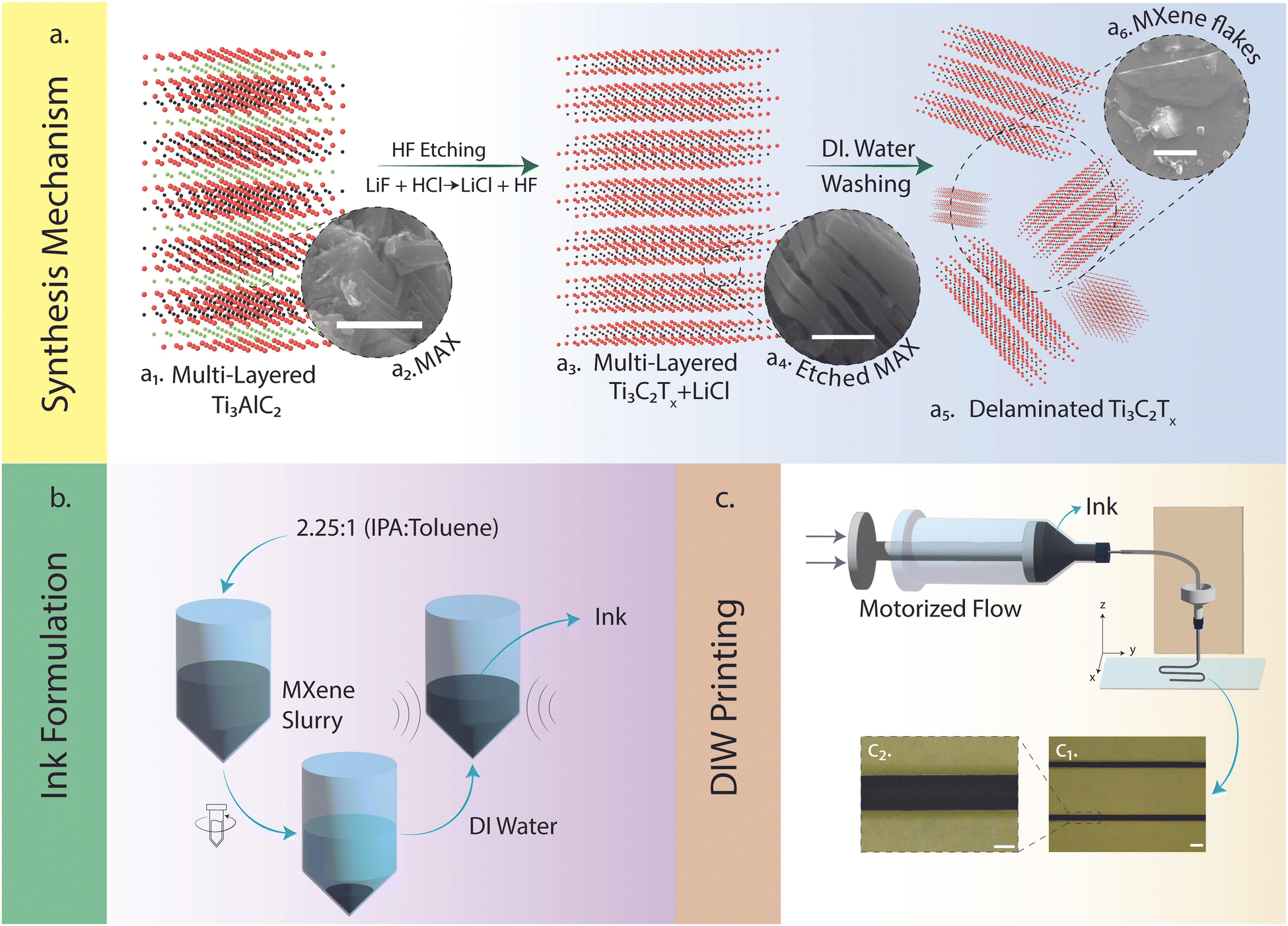 | ||
| Fig. 1 (a) MXene synthesis using the HF etching process. (a1) The multi-layered structure revealing the Al layer in-between layers of Ti3C2. (a2) Representative SEM of MAX phase (scale bar 2 μm). (a3) Multi-layered structure after etching away the Al layer. (a4) Representative SEM of etched MAX (scale bar 500 nm). (a5) Delaminated MXene after repeated washing using DI water. (a6) Representative SEM of MXene flake to show delamination (scale bar 500 nm). (b) Increasing the MXene concentration of the slurry by centrifuging the slurry with antisolvents to remove excess solvent and re-dispersion using the right amount of DI water before sonicating to obtain the ink. (c) DIW to print conductive patterns on PVA coated substrates for potential circuits. (c1) Optical photo capture of a printed line of 100 mg mL−1 MXene in DI water (scale bar 1000 μm). (c2) Zoomed-in optical capture of the printed lines (scale bar 500 μm). | ||
Fig. 2 summarizes the processes of synthesizing Ti3C2Tx from the elemental powders composing its MAX precursor (Ti3AlC2).22,26,27 Titanium, Aluminum, and Titanium Carbide were mixed and ground in their stoichiometric molar amounts (Fig. 2a) for at least 30 min to create a homogenously distributed mixture. The entire milling procedure was performed in a glovebox-provided inert atmosphere to prevent oxidation of the elemental powders. Afterward, the mixture was transferred to the tube furnace in an alumina crucible for heat treatment (Fig. 2b). The sintering procedure was comprised of both the ramp and hold stages. Structural limitations imposed by the glass tube (where the crucible is placed and annealing occurs) constrained the ramping to a rate of 5 °C min−1 (see ESI† for details). The sintered flakes were then milled and strained (Fig. 2c and d) through a 400 mesh sieve to create a uniform-size distribution of fine MAX phase powder (∼35 μm). The equations that describe the formation phase mechanism of these powders are outlined below:28
| Ti + Al → TiAl | (1) |
| 3Ti + Al → Ti3Al | (2) |
| Ti3Al + 2C → Ti3AlC2 | (3) |
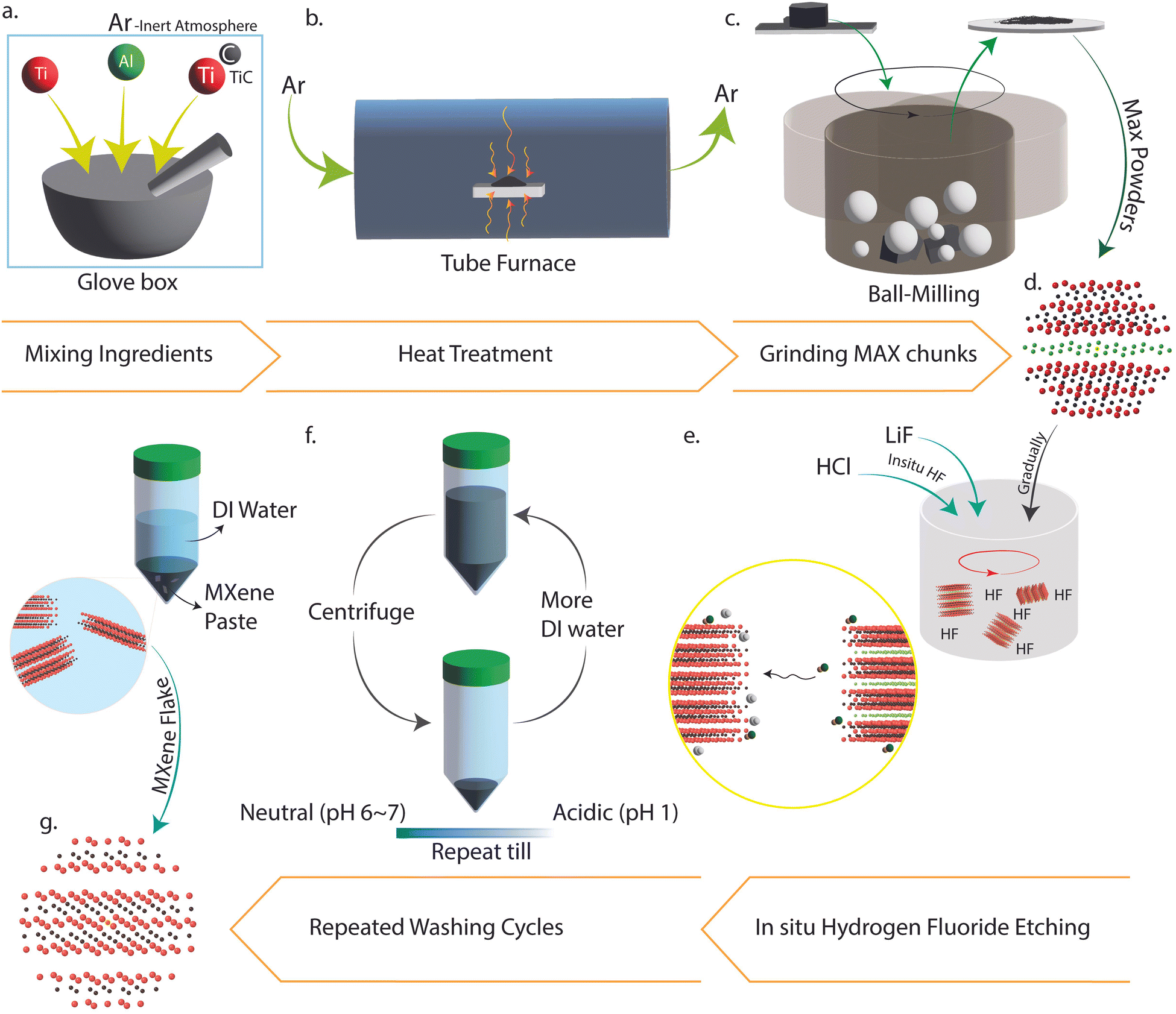 | ||
Fig. 2 The entire process from synthesizing MAX powders to etching out ‘Al’ giving MXene flakes. (a) The ingredients of the MAX phases, Ti3AlC2, (i.e., Ti, Al, TiC) were mixed in the glovebox using mortar and pestle in a molar ratio of 2![[thin space (1/6-em)]](https://www.rsc.org/images/entities/char_2009.gif) :1.1:1, maintaining an Argon atmosphere. (b) The mixture was heat-treated using a tube furnace to initiate the bonding between the different elements. (c) Ball milling broke the large chunks of MAX to form finer-size MAX powders. (d) A representation of the multi-layered crystal structure of MAX. (e) Controlled in situ HF wet etching process to take out the Al layers from Ti3AlC2, giving Ti3C2Tx with the production of acid salts and residual acid. (f) Repeated washing to neutralize the slurry using DI water. (g) A representation of the multi-layered crystal structure of MXene with the Al layer absent. :1.1:1, maintaining an Argon atmosphere. (b) The mixture was heat-treated using a tube furnace to initiate the bonding between the different elements. (c) Ball milling broke the large chunks of MAX to form finer-size MAX powders. (d) A representation of the multi-layered crystal structure of MAX. (e) Controlled in situ HF wet etching process to take out the Al layers from Ti3AlC2, giving Ti3C2Tx with the production of acid salts and residual acid. (f) Repeated washing to neutralize the slurry using DI water. (g) A representation of the multi-layered crystal structure of MXene with the Al layer absent. | ||
In situ HF etching of Ti3AlC2 was the methodology utilized to form its MXene. Equations to illustrate this procedure are highlighted below:24
| LiF + HCl → LiCl + HF | (4) |
| Ti3AlC2 + 3HF → Ti3C2 + AlF3 + 1.5H2 | (5) |
| Ti3C2 + 2H2O → Ti3C2(OH)2 + H2 | (6) |
| Ti3C2 + 2HF → Ti3C2F2 + H2 | (7) |
The MAX powders synthesized (Fig. 2a–d) were etched by hydrofluoric acid generated during the reaction (Fig. 2e), which was produced indirectly through the use of etching agents (i.e., lithium fluoride and hydrochloric acid) significantly reducing the hazards of HF uses.22,27 The acidic nature of the slurry was reduced by dispersing it in deionized water and washing the mixture in a centrifuge till a neutral pH (∼6) was attained (Fig. 2f and g, see ESI,† Fig. S4). A noteworthy highlight during this phase was the stability of the solutions observed during the last cycles, a behavior that was consistent with findings in the literature.29,30
The crystalline characteristics of the synthesized Ti3AlC2 and Ti3C2Tx are illustrated in Fig. 3. As evidenced in Fig. 3a, a thinly packed layered and hexagonal crystalline structure typical of members of the Mn+1AXn family is seen.31 Also notable are kink bands formed due to compression-induced deformation due to ripplocation nucleation.32,33 Furthermore, these kink boundaries allow dislocations to slip along them.31 This improves machinability while preserving damage tolerance.31Fig. 3b–c showcase the P63/mmc spacing group of the Mn+1AXn phase, comprised of edge-sharing MX6 octahedrons mirrored and separated by sheets of A-group elements.31,34 The accordion-like structure of the etched MAX structure is imaged in Fig. 3d. This multi-layered structure was obtained from the supernatant after the procedure performed in Fig. 2f. As we utilized a hybrid of bath/tip (sonication)27 and minimally invasive layer delamination (mild shaking)22,27 methods, the delaminated single-layered Ti3C2Tx flake was then illustrated in Fig. 3e and f. The surface area of the two-dimensional (2D) flake in Fig. 3e and f can be seen to have increased from its three-dimensional (3D) ternary counterpart in Fig. 3a–c. The tapping mode in atomic force microscopy (AFM) described surface topography and other structural characteristics.35 As evidenced by the imaging in Fig. 3g1, the top-view surface of the multi-layered stack in Fig. 3d is shown, as well as its cross-sectional thickness along its x-axis in Fig. 3g2. This confirmed the stacking of ∼80 layers in the multi-layered structure (assuming an average thickness of ∼140 nm and the thickness of a single delaminated sheet = 1.8 nm36). A lateral size of ∼1.412 μm was also obtained (e.g., Fig. 3g1 using ImageJ software), which labels it as a medium-sized flake based on literature classifications.37 The wide-angle X-ray diffraction technique is a primary method to validate and confirm the synthesis of the Ti3AlC2 MAX phase and Ti3C2Tx MXene.38 In Fig. 3h, the MAX crystal peaks were observed. These occurred at 2θ = 9.00° (002), 18.59° (004), 33.52° (101), 36.52° (103), 38.30° (104), 41.26° (105), 47.97° (107), 55.91° (109), 55.96° (110), 64.91° (1011). These intensities were validated using diffraction patterns in past reports, and the peaks appeared as expected.37 MAX phase synthesis was confirmed through the presence of the (104) peak, and successful MXene synthesis was validated through the backward shifting of characteristic (002) and (004) peaks.32 Furthermore, it was also observed that the overall intensities of all phases reduced after the etching was completed. Delaminated single-layer flakes possess diffraction peaks containing only the (002) peak due to the disappearance of all the other phases.27 Multi-layered MAX phases, on the other hand, contain different phases, such as TiC and α-Al2O3.38 Both of these contaminants were formed during the Ti3AlC2 MAX phase synthesis that remained after the etching procedures.38 MXene delamination due to shaking and sonication eliminated these phases due to the filtering and remaining of the accordion-like structure in Fig. 3d.
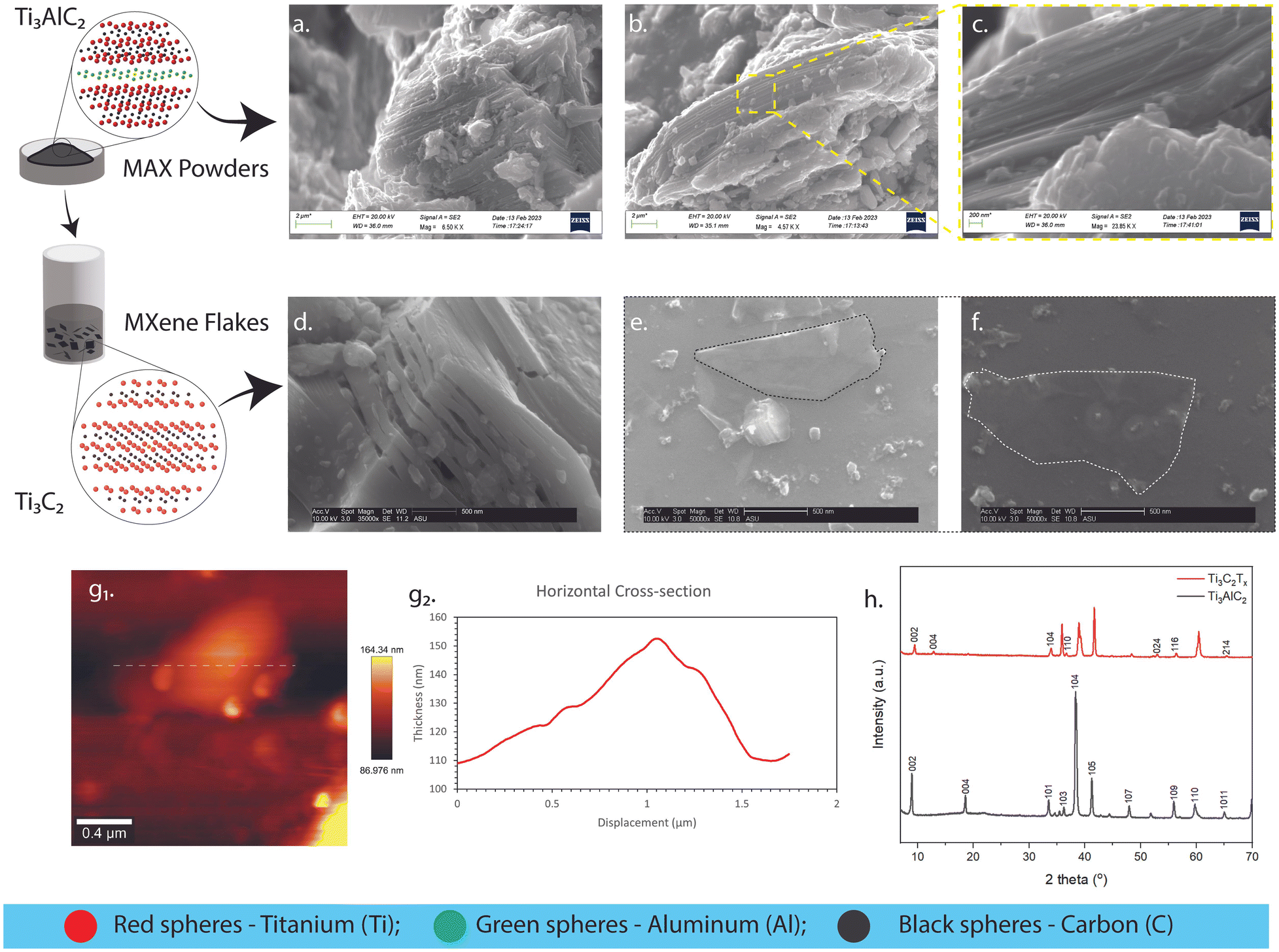 | ||
| Fig. 3 The material characterizations differentiate the MAX phase powders and MXene flakes. (a) and (b) SEM images of MAX phase powders to show the layered stacking, adhering with the illustration of MAX powders (scale bar 2 μm). (c) Zoomed in SEM to highlight the MAX layered structure (scale bar 200 nm). (d) The cross-sectional SEM image of the multi-layered MXene after etching highlights the absence of the Al layer, confirming the successful etching of the precursor (scale bar 500 nm). (e) and (f) Highlight the delaminated MXene flake that was obtained after sonication (scale bar 500 nm). (g1) and (g2) AFM illustrates the thickness of a MXene sample. (h) WAXD patterns illustrate the composition of formed MAX and MXene. The peaks and the intensities are identified and labelled accordingly to showcase the structural change observed when MXene is obtained by further processing MAX. | ||
As mentioned earlier in the report, the unique properties of MXenes (e.g., hydrophilicity, high surface charge due to terminations) allow them to be applied and deposited on different substrates.14,17,19,39 Inks were discovered to be a better avenue for depositing 2D flakes on substrates due to the increased control over layer thickness parameters.39 Consequently, the colloidal solutions containing both multi-layered and delaminated Ti3C2Tx (Fig. 3d and e) were sonicated for an extended period (∼8 h) to ensure solutions contained purely delaminated flakes. Before direct ink writing, the rheological characteristics based on the MXene loading in DI water (10 mg mL−1, 20 mg mL−1, 30 mg mL−1, 50 mg mL−1, 100 mg mL−1, and 200 mg mL−1) were investigated to determine the ideal concentration of the inks for flowing and printing (see ESI,† Fig. S5). As a result, the low concentrations of inks were not considered for further studies (10 mg mL−1 and 20 mg mL−1), deemed hard to control the ink flow. In Fig. 4a, the viscosity of the different concentrations (i.e., 30 mg mL−1, 50 mg mL−1, 100 mg mL−1, and 200 mg mL−1) was analyzed as the shear rate was increased. All four concentrations displayed shear-thinning Non-Newtonian (pseudoplastic) behavior which was desired to ensure continuous flow through the nozzle. Frequency sweep tests were subsequently carried out. As can be seen in Fig. 4b and c, the storage and loss moduli for all the concentrations (i.e., 30 mg mL−1, 50 mg mL−1, 100 mg mL−1, and 200 mg mL−1) were stable (i.e., zero to little fluctuations) for the frequency range (i.e., 10−1–103 rad s−1) studied. This was desirable for these viscoelastic properties as it foretold uniform material deposition and material fidelity on different substrates (i.e., glass, plastic). Ultimately, the higher concentration inks (i.e., 100 mg mL−1 and 200 mg mL−1) were selected due to their linear viscoelastic region as the strain increased. Additionally, the 100 mg mL−1 ink had a difference in its viscoelastic moduli compared to the 200 mg mL−1, hence the former uwas used for the printing and performance. Using a motorized flow dispenser, these inks were printed in straight lines and zig-zag patterns (Fig. 1c and 4d and e). Further process details are highlighted in the methods section (see ESI,† Fig. S5–S7). The electrical conductivity of printed Ti3C2Tx patterns was analyzed with increasing concentration in Fig. 4e. Aqueous MXene inks of all four concentrations were deposited on a glass substrate in circular dots (diameter ≈ 9.15 mm) with a square cross-section (L ≈ 0.05 mm). The resistance of the different depositions was collected using the two-point probe technique (KEITHLEY multimeter). The conductivity values were subsequently calculated using the following equation mentioned below.
| σ = L/RA | (8) |
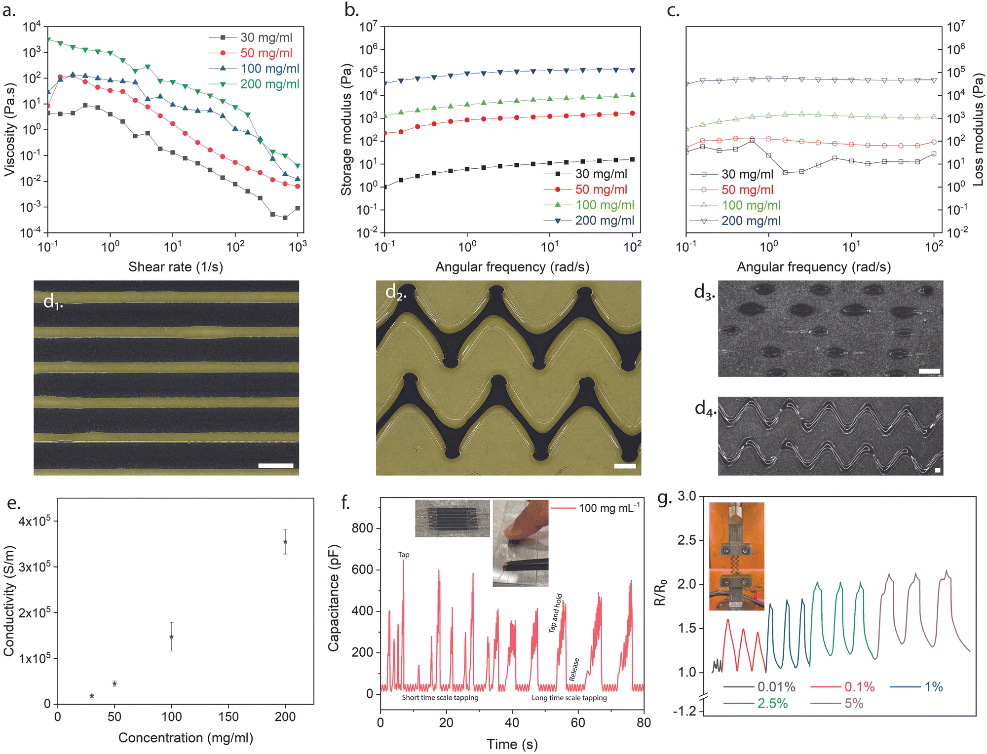 | ||
| Fig. 4 Demonstrative characterizations of Ti3C2Tx inks. (a) Flow sweep test showing the change in viscosity of the ink concentrations with increasing shear rate. (b) and (c) Oscillation frequency test showing variations of storage moduli (G′ and G′′, respectively) against angular frequency. (d1)–(d4) Different patterns of MXene printed using the DIW method (d1) Scale 500 μm; (d2–3) Scale 1000 μm. (e) Conductivity vs. concentration plot of aqueous ink solutions. (f) An interdigitated capacitor with parallel printed lines of MXene displaying capacitive sensing responding to index finger. (g) Strain sensing performance at strain loading from 0.01–5%. | ||
Additionally, Fig. 4f displays the behavior of an interdigitated capacitor arrangement made of MXene material when a finger touches it. The capacitance of the structure rapidly increases as soon as the finger touches the surface, indicating a highly sensitive response. This occurs because the separation distance between the interdigitated electrodes decreases when the finger comes into contact with the surface, resulting in increased capacitance. The sensor's sensitive response can detect short-timescale and long-timescale touches. This sensitivity is desirable for applications such as touch sensors and human-machine interfaces, where a responsive and accurate touch response is essential.
The conductivity of MXene on PVA changes with increasing strain loading (Fig. 4g) because the mechanical deformation of the substrate alters the distance between the MXene flakes, affecting the inter-flake distance and the degree of overlap between the flakes. As the substrate is stretched, the MXene flakes become elongated and reoriented, leading to changes in the electrical conductivity. As the spacing between the flakes increases with strain, the degree of overlap decreases, resulting in a decrease in conductivity. Conversely, as the spacing between the flakes decreases, the degree of overlap increases, increasing conductivity. Thus, the change in conductivity of MXene on PVA with increasing strain loading results in the interplay between the mechanical deformation of the substrate and the intrinsic electrical properties of the MXene flakes.
In summary, 2D MXene nanoparticles, a young family of materials with promising applications, have shown enormous potential in conductive inks and printable electronics. We have demonstrated the controllability of the MXene synthesis, the ink formulations of these materials, and their 3D printability for electronic and energy device industries. Consequently, simple 3D printing has shown enhanced processability via ink writing compared to conventional stamping or microcontact molding. Specifically, we were not only able to perform an in-house synthesis of Ti3C2Tx but also perform programmable microstructures of aqueous dispersions. This allowed us to control selective material depositions and create high-resolution micropatterns precisely. Also, the MXene concentrations required to produce these free-standing architectures were higher than inkjet-based 3D printing, benefiting manufacturing scalability and productivity. Finally, we showed good electrical and electrochemical properties of the fabricated patterns. With a limitation to micropatterning, further studies must be done to increase the synthesis yield and printing precision to achieve nanoscale feature control and unlock the full potential of MXenes for broader applications.
Author contributions
M. Fagade and K. Song conceptualized and designed a research objective, as well as drafted the manuscript; M. Fagade, D. Patil, D. Ravichandran, S. Thummalapalli, S. Jambhulkar performed experiments; M. Fagade analyzed results, performed theoretical calculations, and drafted the manuscript; and D. Patil conducted the 3D printing setup and performed printing. All authors reviewed the final manuscript.Conflicts of interest
There are no conflicts to declare.Acknowledgements
We acknowledge the financial support from the NSF CAREER (#2145895), AFOSR (#FA9550-22-1-0263), BSF (#2020102), and ACS PRF (#62371-ND10).References
- I. C. L. Ng and S. Y. L. Wakenshaw, Int. J. Res. Mark., 2017, 34, 3–21 CrossRef.
- S. Shajari, S. Ramakrishnan, K. Karan, L. J. Sudak and U. Sundararaj, Appl. Mater. Today, 2022, 26, 101295 CrossRef.
- A. Ghaffarkhah, M. Kamkar, Z. A. Dijvejin, H. Riazi, S. Ghaderi, K. Golovin, M. Soroush and M. Arjmand, Carbon, 2022, 191, 277–289 CrossRef CAS.
- Q. Jiang, Y. Lei, H. Liang, K. Xi, C. Xia and H. N. Alshareef, Energy Storage Mater., 2020, 27, 78–95 CrossRef.
- Y. Aleeva and B. Pignataro, J. Mater. Chem. C, 2014, 2, 6436–6453 RSC.
- M. Cavallini, J. Mater. Chem., 2009, 19, 6085–6092 RSC.
- M. Cavallini, P. D’Angelo, V. V. Criado, D. Gentili, A. Shehu, F. Leonardi, S. Milita, F. Liscio and F. Biscarini, Adv. Mater., 2011, 23, 5091–5097 CrossRef CAS PubMed.
- J. A. Lewis, J. E. Smay, J. Stuecker and J. Cesarano, J. Am. Ceram. Soc., 2006, 89, 3599–3609 CrossRef CAS.
- C. H. Kim, J. Jo and S.-H. Lee, Rev. Sci. Instrum., 2012, 83, 065001 CrossRef PubMed.
- A. Perl, D. N. Reinhoudt and J. Huskens, Adv. Mater., 2009, 21, 2257–2268 CrossRef CAS.
- H. Schift, J. Vac. Sci. Technol., B: Microelectron. Nanometer Struct.–Process., Meas., Phenom., 2008, 26, 458–480 CrossRef CAS.
- J. Ma, S. Zheng, Y. Cao, Y. Zhu, P. Das, H. Wang, Y. Liu, J. Wang, L. Chi, S. (Frank) Liu and Z.-S. Wu, Adv. Energy Mater., 2021, 11, 2100746 CrossRef CAS.
- P. Jiang, Z. Ji, X. Zhang, Z. Liu and X. Wang, Prog. Addit. Manuf., 2018, 3, 65–86 CrossRef.
- Z. Aghayar, M. Malaki and Y. Zhang, Nanomaterials, 2022, 12, 4346 CrossRef CAS PubMed.
- L. Li, J. Meng, X. Bao, Y. Huang, X.-P. Yan, H.-L. Qian, C. Zhang and T. Liu, Adv. Energy Mater., 2023, 13, 2203683 CrossRef CAS.
- H. Y. Jun, S. O. Ryu, S. H. Kim, J. Y. Kim, C.-H. Chang, S. O. Ryu and C.-H. Choi, Adv. Electron. Mater., 2021, 7, 2100577 CrossRef CAS.
- Y. Gogotsi and B. Anasori, ACS Nano, 2019, 13, 8491–8494 CrossRef CAS PubMed.
- M. Naguib, V. N. Mochalin, M. W. Barsoum and Y. Gogotsi, Adv. Mater., 2014, 26, 992–1005 CrossRef CAS PubMed.
- W. Y. Chen, X. Jiang, S.-N. Lai, D. Peroulis and L. Stanciu, Nat. Commun., 2020, 11, 1302 CrossRef CAS PubMed.
- H. Wang, Y. Wu, J. Zhang, G. Li, H. Huang, X. Zhang and Q. Jiang, Mater. Lett., 2015, 160, 537–540 CrossRef CAS.
- M. Khazaei, A. Ranjbar, M. Arai, T. Sasaki and S. Yunoki, J. Mater. Chem. C, 2017, 5, 2488–2503 RSC.
- S. Jambhulkar, S. Liu, P. Vala, W. Xu, D. Ravichandran, Y. Zhu, K. Bi, Q. Nian, X. Chen and K. Song, ACS Nano, 2021, 15, 12057–12068 CrossRef CAS PubMed.
- S. Jambhulkar, D. Ravichandran, B. Sundaravadivelan and K. Song, J. Mater. Chem. C, 2023, 11, 4333–4341 RSC.
- W. Yang, J. Yang, J. J. Byun, F. P. Moissinac, J. Xu, S. J. Haigh, M. Domingos, M. A. Bissett, R. A. W. Dryfe and S. Barg, Adv. Mater., 2019, 31, 1902725 CrossRef PubMed.
- J. Orangi, F. Hamade, V. A. Davis and M. Beidaghi, ACS Nano, 2020, 14, 640–650 CrossRef CAS PubMed.
- K. Lu, Int. Mater. Rev., 2008, 53, 21–38 CrossRef CAS.
- M. Alhabeb, K. Maleski, B. Anasori, P. Lelyukh, L. Clark, S. Sin and Y. Gogotsi, Chem. Mater., 2017, 29, 7633–7644 CrossRef CAS.
- Y. Liu, C. Wang, W. Luo, L. Bai, Y. Xu, X. Hao, J. Zhu and S. Guo, J. Adv. Ceram., 2022, 11, 1491–1497 CrossRef CAS.
- C. E. Shuck, A. Sarycheva, M. Anayee, A. Levitt, Y. Zhu, S. Uzun, V. Balitskiy, V. Zahorodna, O. Gogotsi and Y. Gogotsi, Adv. Eng. Mater., 2020, 22, 1901241 CrossRef CAS.
- T. Zhang, L. Pan, H. Tang, F. Du, Y. Guo, T. Qiu and J. Yang, J. Alloys Compd., 2017, 695, 818–826 CrossRef CAS.
- M. Beckers, N. Schell, R. M. S. Martins, A. Mücklich, W. Möller and L. Hultman, J. Appl. Phys., 2007, 102, 074916 CrossRef.
- M. Sokol, V. Natu, S. Kota and M. W. Barsoum, Spec. Issue Part Two Big Quest. Chem., 2019, 1, 210–223 CAS.
- M. W. Barsoum, X. Zhao, S. Shanazarov, A. Romanchuk, S. Koumlis, S. J. Pagano, L. Lamberson and G. J. Tucker, Phys. Rev. Mater., 2019, 3, 013602 CrossRef CAS.
- P. O. Å. Persson, S. Kodambaka, I. Petrov and L. Hultman, Acta Mater., 2007, 55, 4401–4407 CrossRef CAS.
- S. S. Ray, Environmentally friendly polymer nanocomposites: types, processing and properties, Elsevier, 2013 Search PubMed.
- A. C. Y. Yuen, T. B. Y. Chen, B. Lin, W. Yang, I. I. Kabir, I. M. D. C. Cordeiro, A. E. Whitten, J. Mata, B. Yu and H.-D. Lu, Compos. Part C Open Access, 2021, 5, 100155 CrossRef CAS.
- S. Uzun, M. Schelling, K. Hantanasirisakul, T. S. Mathis, R. Askeland, G. Dion and Y. Gogotsi, Small, 2021, 17, 2006376 CrossRef CAS.
- B. Scheibe, V. Kupka, B. Peplińska, M. Jarek and K. Tadyszak, Materials, 2019, 12, 353 CrossRef CAS PubMed.
- S.-H. Seok, S. Choo, J. Kwak, H. Ju, J.-H. Han, W.-S. Kang, J. Lee, S.-Y. Kim, D. H. Lee and J. Lee, SAMSUNG, Korea Semiconductor Industry Association (KSIA), Korea Semiconductor Research Association (COSAR), 2021.
Footnotes |
| † Electronic supplementary information (ESI) available. See DOI: https://doi.org/10.1039/d3ma00096f |
| ‡ Co-first authors. |
| This journal is © The Royal Society of Chemistry 2023 |