
 Open Access Article
 This Open Access Article is licensed under a Creative Commons Attribution-Non Commercial 3.0 Unported Licence
Soft grafting of DNA over hexagonal copper sulfide for low-power memristor switching†
Smita Gajanan
Naik
 a,
M. K.
Rabinal
*b and
Shouvik
Datta
c
a,
M. K.
Rabinal
*b and
Shouvik
Datta
c
aDepartment of Physics and Electronics, Christ University, Bengaluru, Karnataka-560029, India
bDepartment of Physics, Karnatak University, Dharwad – 03, India. E-mail: mkrabinal@yahoo.com
cDepartment of Physics, Indian Institute of Science Education and Research, Pune, India
First published on 30th September 2023
Abstract
Green electronics, where functional organic/bio-materials that are biocompatible and easily disposable are implemented in electronic devices, have gained profound interest. DNA is the best biomolecule in existence that shows data storage capacity, in virtue of the sequential arrangement of AT and GC base pairs, analogous to the coding of binary numbers in computers. In the present work, a robust, uniform and repeatable room-temperature resistive switching in a Cu/Cu2S/DNA/Au heterojunction is demonstrated. The DNA nanostructures were anchored on the densely packed hexagonal Cu2S structures by simple electrochemical deposition. This heterostructure presents outstanding memristor behavior; the device exhibits resistive switching at a very low threshold voltage of 0.2 V and has a relatively high ON/OFF ratio of more than 102 with a good cycling stability of ∼1000 cycles and a negligible amount of variation. The justification for such a switching mechanism is also given on the basis of the energy-band diagram of the Cu2S–DNA interface. Based on the studies herein, the resistive switching is attributed to the reversible doping of DNA by Cu+ ions, leading to intrinsic trap states. Further, the switching is modeled with the help of different transport mechanisms, like Schottky-barrier emission, Poole–Frenkel emission and Fowler–Nordheim tunneling.
1. Introduction
In the last decade, digital technology has developed dramatically and data storage requirements have reached an unprecedented scale. The conventional transistor-based memory technology is facing a shortfall in meeting future needs and the drive for development of high-density storage devices has increased. Meanwhile, resistive-switching devices are being contemplated as the future of memory technology, as they have promising features like a simple device architecture, high memory density, cycling stability, fast switching, and good endurance at ultra-low power consumption.1 Due to their high data storage density, switching devices could become game changers for quantum computing, neural networks, artificial synapses, etc.2 The devices have metal–active-layer–metal cross-bar structures (active layer: insulators, semiconductors, organic molecules, etc.) which toggle between the high-resistance state (HRS) and low-resistance state (LRS) under external electric stimuli. The change in the resistive states helps these devices to store memory, hence they are also termed as “memristors” (memory + resistor). The electrical switching can happen in both directions (HRS-to-LRS or LRS-to-HRS); the former is more conventional as compared to the latter.3,4 The latter devices are referred to as negative differential resistance memristors, and the effect is rarely observed.5 Based on voltage control, memristors are further classified as having unipolar, bipolar and threshold switching. In the first one, the resistive switching occurs under the same voltage polarity; in the second one, the ON/OFF switching occurs under opposite voltage polarities; and in the third one, switching sharply occurs at a particular voltage and that minimum voltage is essential to maintaining the device in the ON state.6Resistive switching has been predominantly observed in metal oxides and amorphous semiconductors since almost six decades ago,7 but recently switching in 2D-metal chalcogenides,8,9 carbon nanostructures,10,11 perovskites,12–15 binary transition-metal oxides16–18 and even biomaterials has been investigated.19–22 Recently, a new class of the memristors called ‘gasistors’ have drawn attention for their dual role in gas sensing and memory applications; ultrasensitive detection of gases by switching of states is observed in materials like sulfides and some oxides.23–26 Very crucially, inorganic functional materials leave toxic non-degradable waste, which impact the lives of future generations, and the continuous supply of inorganic functional materials in the future is next to impossible. Hence, the use of biomaterials is the green solution for the growth of the electronics industry. Bioelectronics give synergistic effects of biomaterials and electronics; the biomaterials will lead to sustainable, low-cost and eco-friendly technology. The biocompatibility, transparency and highly flexible nature, and also other added advantages like easy processing and simple extraction, are some of the important properties that are not observed in inorganic materials. Because of all these points, biomaterials are very important for special-purpose applications in the military, bioelectronics, medicine, etc. Hence, recently a number of biomaterials like saccharides, silk, proteins, peptides, nucleobases, egg albumins, etc. have been explored for resistive-switching applications.22,27
Amongst these, deoxyribonucleic acid (DNA) is trending because of its unique double-helical structure. Its structure comprises long twisted strings of sugar-phosphate chains connected through AT/GC base pairs (A – adenine, T – thymine, G – guanine and C – cytosine); the sequence of AT and GC is analogous to the coding of binary numbers in computers.28,29 It is the best nanowire in natural existence, the cost of individual nucleo-bases is a few US cents, and it has benefits like self assembly, self replication and the capacity to adopt various conformers. Intrinsic DNA is electrically poorly conducting (insulating) but insertion of metal ions within the base pairs of this molecule appreciably enhances its electrical conductivity and hence makes such materials suitable in the design of bioelectronics.30,31 This is one important key point for using DNA in resistive-switching devices; the electric-field enhanced mobility of the ions within the intrinsic states of the DNA will lead to resistive switching. Based on these special features of DNA, it is tentatively predicted that this molecule could store a large amount of data in a small volume, probably up to 215 petabytes in a gram quantity.32 It is also very important to explore the intrinsic electronic function of biomaterials for device applications; this is usually achieved either by doping or by creating interfaces with inorganic materials. According to the literature, DNA assembly with inorganic semiconductors will provide complementary features, with low-power switching characteristics and enhancement in the RON–ROFF ratio. Serious efforts to couple DNA molecules with semiconductors/metals to create interesting electronic interfaces are underway.33,34
In this regard, metal sulfides have recently been explored to design unique interfaces;35,36 in particular, those with layered 2D semiconductors like MoS2 and WS2 have been studied to develop unipolar/bipolar memristors with a thickness reduction to mono-/few-layer materials.37 Thus, there is a strict need for the development of multifunctional, environmentally viable materials for memristive applications. Copper-based semiconductors are considered as important members of the inorganic family considering their sustainability along with clean and green features. Copper metal is abundant, low-cost and easy to process into thin-foil form. In the present work, one such attempt to form a flexible memory device based on a copper-sulfide–DNA heterointerface using copper foil is carried out. The formation of the Cu2S is achieved by a simple and cost effective method of dip-coating. Following this, the copper sulfide interface with DNA is formed by the electrodeposition method, which ensures thin uniform film formation of a desired thickness, which is highly needed for device applications. The present work offers a unique, simple and economic method of memristor device fabrication. The device exhibits a good ON–OFF ratio and stability and ultra-low-power functionality.
2. Experiment details
2.1. Chemicals used
A thin copper plate (with purity 99.99%) of 0.2 mm thickness was obtained commercially and used as a source of copper. The sulfur powder was obtained from SD-Fine Chemicals India, and hydrazine hydrate (NH2NH2·H2O) was obtained from HiMedia Laboratories, India. All the chemicals used for synthesis are of analytical grade without any further purification. Throughout the experiments, deionized water (DI) is used.2.2. Preparation of the copper sulfide–DNA heterostructure
A simple two-step deposition was adopted for this preparation. Firstly, a sulfur–hydrazine-hydrate complex solution was prepared by adding 0.02 g of sulfur powder to 1 ml hydrazine hydrate, then diluting it by adding 4 ml DI water. A very-well-cleaned copper substrate of 2 cm2 was taken; a flexible plastic sticker (commercially available), with good chemical resistivity and a pattern of round holes 0.15 mm in diameter, was placed on the copper substrate and pressed uniformly to achieve a good adherence. Later, this plate was dipped in the sulfur solution; immediately after dipping, the color of the copper plate changes to gray-black. It was kept in the chemical bath for 1 min for the reaction to complete. The plate was rinsed with DI water many times and dried under a table lamp. The formation of the copper sulfide was confirmed by X-ray diffraction (XRD) and scanning electron microscopy (SEM) measurements, which will be discussed later.Further, as a second step, the dried Cu plate with deposited copper sulfide was used for the electrodeposition of DNA. For this, a 0.01 M DNA solution in 10 ml of DI water was prepared as the electrolyte and platinum wire was used as the counter electrode. A very small current of 50 μA was made to pass through the solution for one hour by making the Cu positive and platinum negative. Formation of a thin DNA layer on the copper sulfide could be visualized and was also confirmed by SEM analysis. A Keithly 2636A source meter interfaced with the Lab-VIEW program was used for electrical characterization. A home-built conductivity setup was used for forming electrical contacts; the copper plate was used as the bottom electrode while fine gold wire was used to form a contact with the DNA.
3. Results and discussion
Fig. 1 shows a pictorial representation of the experimental details, showing the simplicity of the technique and details of the fabrication of the Cu2S–DNA heterostructure for a memristor. As mentioned earlier, the method gives the quick formation of multiple dots of Cu2S. Our group previously proposed this simple method of formation of a copper sulfide film over copper by simple dip chemistry at room temperature.38 These nanostructures are successfully utilized for thermoelectric and supercapacitor applications. The film formation mechanism is clearly discussed in this report. The formation involves the sulfur dissolved in hydrazine hydrate helping to form an air-stable sulfur–hydrazine-hydrate complex, which slowly releases S2− anions to react with copper, resulting in formation of copper sulfide. The method is quite simple and economically viable for tuning the structure and stoichiometry of the resulting materials through the adjustment of the temperature and concentration of the chemical bath. The proposed reaction is given below as eqn (1).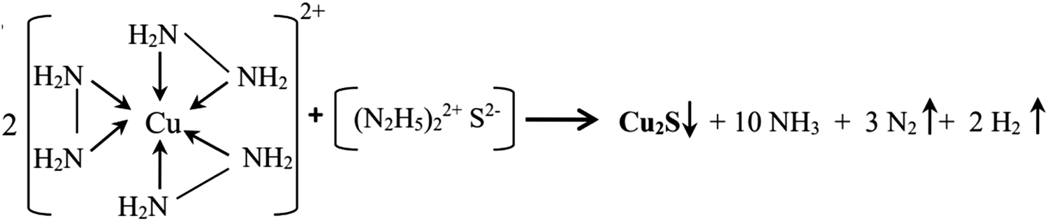 | (1) |
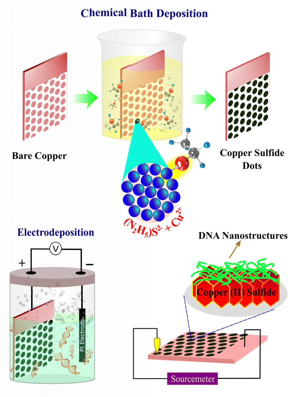 | ||
| Fig. 1 Schematic illustration of electroless and electrochemical syntheses of Cu2S and DNA on the Cu substrate and finally the constitution of the Cu/Cu2S–DNA/Au junction. | ||
The thickness of the films was measured by using a Mitutoya precision gauge; the measured thicknesses are 40 μm and 55 μm for Cu2S and DNA, respectively. The XRD analysis of the electroless deposited copper sulfide dots was carried out for scattering angles (2θ) ranging from 20° to 80°; the recorded spectrum is given in Fig. 2. Diffraction peaks with Miller indices (0 0 4), (1 11 1), (1 7 4), (2 13 1) and (2 4 0) are observed, and correspond to the standard peak patterns of the monoclinic Cu2S phase (JCPDS no. 23-0961). No extra peaks are observed along with the monoclinic Cu2S phase peaks. The results reveal that pure monoclinic Cu2S dots are formed on the copper plate after sulfurization, with lattice parameters a = 13.50 Å, b = 27.32 Å and c = 11.8 Å. Further, the surface morphology of these films is analysed using FESEM measurements; the presence of DNA on Cu2S can be clearly observed, as shown in Fig. 3(a) and (b). Interestingly these images show a clear difference; in the case of Cu2S, uniform 3D hexagonal structures over the copper substrate are observed. Densely packed hexagonal structures with an average size of 1 μm can be seen. Subsequently, the high-resolution images show worm-like structures of DNA on the Cu2S surface. The chemical composition observed for the Cu2S films using the X-ray energy dispersive spectroscopy technique is close to the standard stoichiometric composition, that is Cu![[thin space (1/6-em)]](https://www.rsc.org/images/entities/char_2009.gif) :S: 2:1.
:S: 2:1.
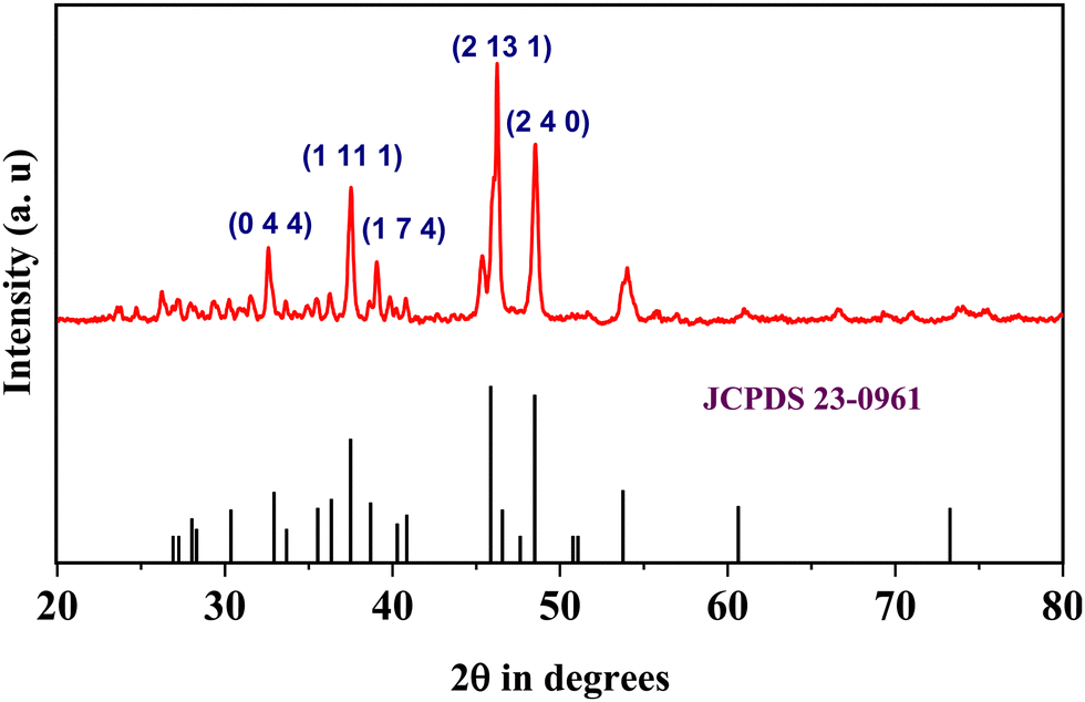 | ||
| Fig. 2 XRD pattern of deposited copper sulfide matched with JCPDS 23-0961. | ||
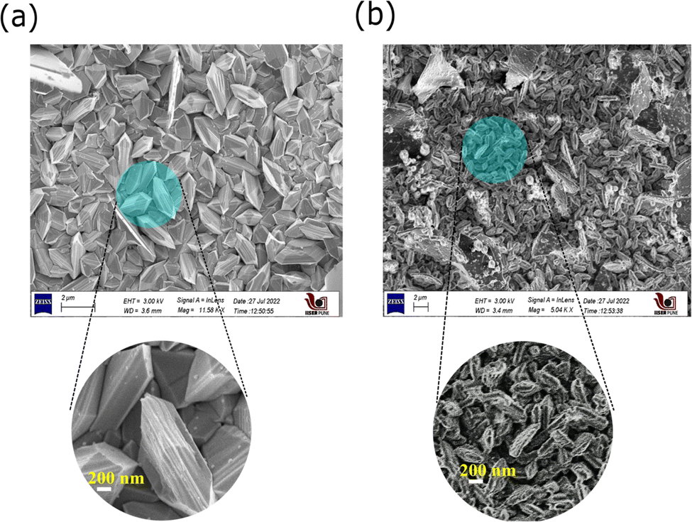 | ||
| Fig. 3 High-resolution SEM images of (a) copper sulfide and (b) copper sulfide with deposited DNA. | ||
Current–voltage (I–V) curves of these heterostructures are recorded by using our home-built conductivity setup.40 Here, the Cu plate is used as the bottom contact and gold wire of diameter 4.91 × 10⁻⁴ cm2 as the top contact; a schematic view of the device configuration is shown as the last cartoon in Fig. 1. These curves are recorded in a cyclic order; the voltage sweep is carried out from 0 V → +1 V, +1 V → 0 V, 0 V → −1 V, and −1 V → 0 V as one cycle. For comparison, the I–V curves were first recorded for the bare materials, with Cu/Cu2S/Au and Cu/DNA/Au junctions at room temperature. Fig. 4 shows the typical I–V curves of these junctions along with the curve for direct contact between Cu–Au junctions. For all the junctions in the present measurements, the forward bias (first quadrant) means the bottom Cu electrode is positive with respect to the top Au point-contact. The reverse bias (third quadrant) means Cu is negative and the Au electrode is positive.
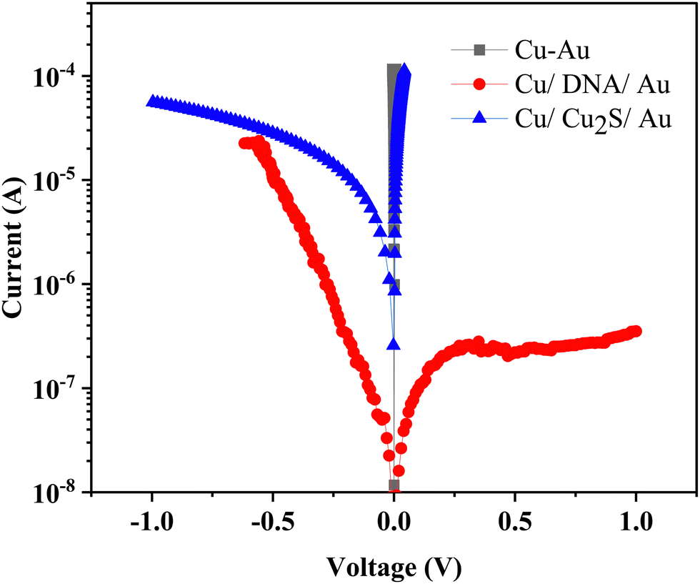 | ||
| Fig. 4 Comparison of I–V curves of Cu/Au, Cu/DNA/Au and Cu/Cu2S/Au junctions. | ||
It is observed that the Cu–Au junction shows shorting of the two metals, whereas the other two junctions show rectification. There is a good rectification in the Cu/Cu2S/Au junction; it conducts more in the first quadrant and less in the third quadrant. However, an opposite rectification effect is observed in the case of the Cu/DNA/Au junction. Such behaviors can be easily understood on the basis of the energy-band diagram of these interfaces, which has been reported earlier by us and also by others.40,41 During current–voltage scans in these junctions, no electrical switching has been observed. Typically, the Cu2S phase becomes a self-doped p-type semiconductor with high intrinsic conductivity leading to Ohmic (linear) behavior.38 However, there are a couple of reports that claim electrical switching in bare copper sulfides due to the intrinsic nature of the material. DNA as a rectifier has been well reported and its combinations with other semiconductors are predicted as good active materials for memristors.37 The recent work on DNA rectification through the insertion of a foreign molecule has coined the term “World's Smallest Diode”.41
Subsequently, similar current–voltage measurements were carried out for the Cu/Cu2S:DNA/Au multiple junction at room temperature by sweeping the voltage (0 V → +0.5 V, +0.5 V → 0 V, 0 V → −0.5 V, and −0.5 V → 0 V). For a clear depiction, the semi-logarithmic plots of these measurements are shown in Fig. 5(a); here, the arrows indicate the sweeping direction and are labeled as paths I, II and III for convenience. The application of the bias voltage in the positive direction first increases the current with voltage (path I). The device initially adopts a high-resistance state (HRS) and after reaching a very low critical voltage of 0.2 V, the junction suddenly switches to the low-resistance state (LRS), which is referred to as the SET process. On a further increase in voltage, the junction continues to be in a high-conductivity state (path II). On reversing the voltage, the current decreases on the same path up to the threshold voltage; on further decreasing the voltage towards zero, a distinct high-conductivity path is followed. On reaching a low voltage, close to 0.01 V, the junction suddenly switches to the HRS. In the reverse (negative) bias region, there is no electrical switching at all (path III); instead the device follows a path close to the LRS of the first quadrant (path II).
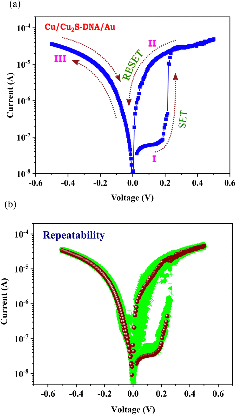 | ||
| Fig. 5 (a) Memristor current–voltage curve of Cu/Cu2S/DNA/Au junction, here arrows show directions of scan. (b) Repeatability curves of a junction for 30 cycles. | ||
This is a typical threshold electrical switching behavior where the SET and RESET occur with a positive voltage. Further, this threshold switching is confirmed by carrying out voltage sweeps only along positive bias, i.e. 0 V → +0.5 V, +0.5 V → 0 V; the behavior was repeatable under this condition (data is not shown). In both full cycle and half positive cycle measurements, the device exhibits a memory window with an ON/OFF ratio of ∼102 and high cycling stability. The repeatability curves up to 1000 cycles have been measured and the data of 30 cycles is shown in Fig. 5(b). The evolution of the switching up to 1000 cycles is also shown in the ESI† as Fig. S1.
The endurance and retention measurements are shown in Fig. 6(a) and (b), respectively. These curves are quite reproducible with a small variation. The resistance of the LRS is 1 × 10⁴ and that of the HRS is 2 × 10⁶. The device-to-device repeatability was checked by carrying out measurements on various junctions; the variation is very small, as shown in Fig. 7. These measurements clearly suggest that Cu2S–DNA heterostructures could be ideally suited for threshold memristor applications; the device exhibits a good endurance and ON/OFF ratio as compared to the recently reported oxides and chalcogenide-based memristors.42–45
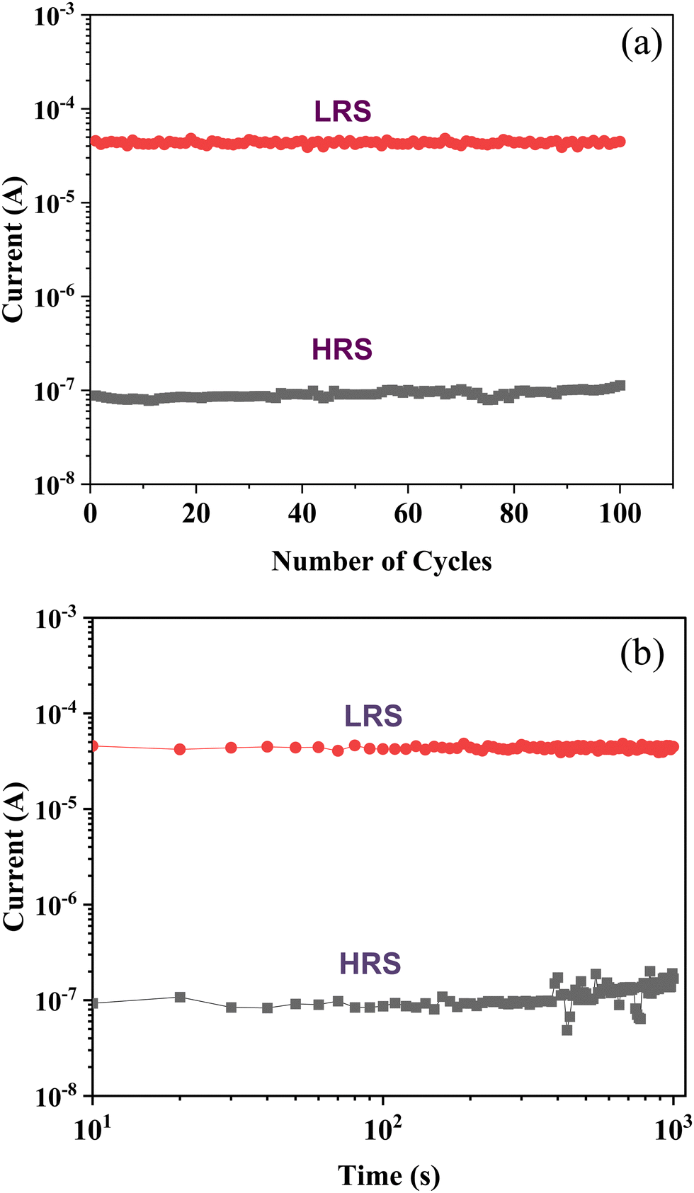 | ||
| Fig. 6 Typical (a) endurance and (b) retention performance of the Cu/Cu2S/DNA/Au junction. | ||
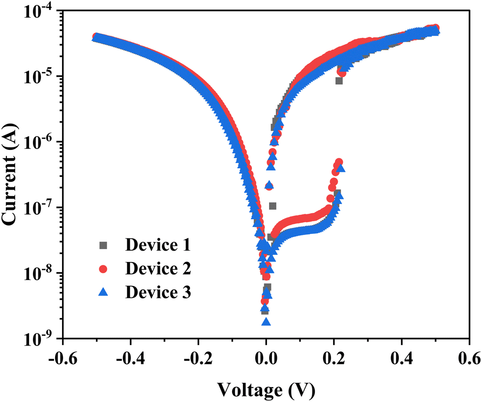 | ||
| Fig. 7 Device-to-device variation of Cu/Cu2S/DNA/Au junctions. | ||
An attempt has been made to understand the charge transport, particularly the electrical switching in the Cu/Cu2S–DNA/Au interface, by drawing its energy-band diagram, which is shown in Fig. 8. To construct this diagram, the work functions of Au and Cu have been taken as 5.1 eV and 4.7 eV, respectively.46,47 The separation between the highest unoccupied molecular orbital (HUMO) and the lowest occupied molecular orbital (LOMO) is taken as 3.75 eV, which corresponds to the Π–Π* stacking of guanine orbitals, and the position of the HUMO with respect to the vacuum level is 3.2 eV.39 Cu2S has a bandgap of 1.47 eV and the conduction band is positioned 4.2 eV below the vacuum level.48 With these parameters, the energy-band diagram looks like that shown in Fig. 8. Under the forward bias of the junction, the Cu is positive and the top Au wire is negative, and hence under this condition electrons flow from right to left with an energy barrier close to 2 eV. At first, with an increase in applied voltage the device follows the HRS (path A) up to 0.2 V in the positive bias region. In this low-conductivity (OFF) state, the current is low and the electron transport has to follow barrier emission to move from Au to DNA, then to Cu2S and finally to Cu (path A).
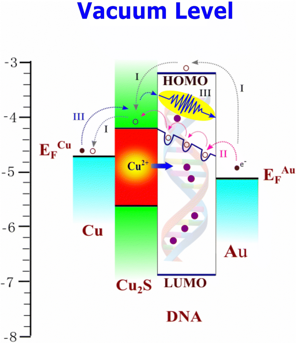 | ||
| Fig. 8 Energy-band diagram of the Cu/Cu2S/DNA/Au junction, indicating various paths of charge transport. | ||
To check this, the experimental data of this regime is plotted for Schottky-barrier emission as ln(I) versus V1/2, as shown in Fig. 9(a). Except for a small scattering of the data, a good fit is observed, showing that the electron transport from right to left is by Schottky-barrier emission. A further increase in voltage across the junction causes the migration of the Cu+ ions from Cu2S into the thin DNA layer. Such cation migration in bulk semiconductors is a quite well-reported topic in the literature49,50 Migration of Cu+ and Ag+ in many bulk chalcogenides and metal oxides has been studied, and this phenomenon has been explored in the electric-field-assisted creation of active electronic devices and in the development of solid-state electrochemical batteries.51 The Cu2S is a self-doped p-type semiconductor with a sufficient number of interstitial Cu+ ions as defects. A very high diffusion coefficient of these ions, close to 2.18 × 10⁻⁸ cm2 s−1, has been reported for Cu2−xS (with x varying from 0–0.06).38 The variation of the composition alters its room-temperature ionic conductivity from 0.07 (ohm cm)−1 to 2500 (ohm cm)−1. Due to the size, density and flexibility of the lattice, these ions in Cu2S can easily migrate under the applied electric field towards the cathode. Due to these factors, the Cu+ ions enter the DNA structure as a dopant and hence enhance its electrical conductivity. So, DNA with a wide band gap of 3.75 eV acquires deep electron-trap states, as shown in Fig. 8. Such insertion of metal ions into DNA base pairs has been well reported in the literature with respect to Ni2+, Cu+, Mg2+, etc.52 These studies claim that under such conditions, the ion-doped DNA shows peculiar semiconductor-to-metallic behavior. In the past, our group has demonstrated an interesting electrical switching effect in the case of PbS:DNA composite films through Pb2+ ion doping in DNA via a reduction/oxidation process.39
With an increase in voltage in the present device, the initial Schottky-barrier emission process switches to Poole–Frenkel defect-assisted emission processes (path B, grey dotted lines in Fig. 8). The experimental data of this regime (from 0.2–0.5 V) has been tested for this process by plotting ln(I/V) versus V1/2; this has been shown in Fig. 9(b) and there is a good agreement. As a result the device sharply switches from the HRS to LRS in the positive quadrant. On decreasing the applied voltage in the positive quadrant the re-doping of DNA takes place by migration of Cu+ ions back into Cu2S, which makes the device go back to its original state below 0.02 V. On reverse bias, the Cu becomes negative and Au positive; the electrons will migrate from Cu to Au through the Cu2S–DNA interface by the process of barrier emission followed by barrier tunneling. Under these conditions, an electron faces a barrier of 0.6 eV to move into Cu2S and then tunnel to Au through the thin-layer DNA (path C, blue lines in Fig. 8). The reverse bias data has been tested for a direct Fowler–Nordheim tunneling process by plotting ln(I/V2) versus 1/V; a good agreement has been noted (Fig. 9(c)). It is concluded that the electrical switching under forward bias occurs by virtue of a change in charge transport from a high-barrier Schottky emission (LRS) to Poole–Frenkel trap-assisted emission (HRS) by electric-field-assisted doping of DNA by Cu+ ions from the Cu2S phase. Under reverse bias, the charge transport is low-barrier emission followed by direct Fowler–Nordheim tunneling through the thin DNA layer.
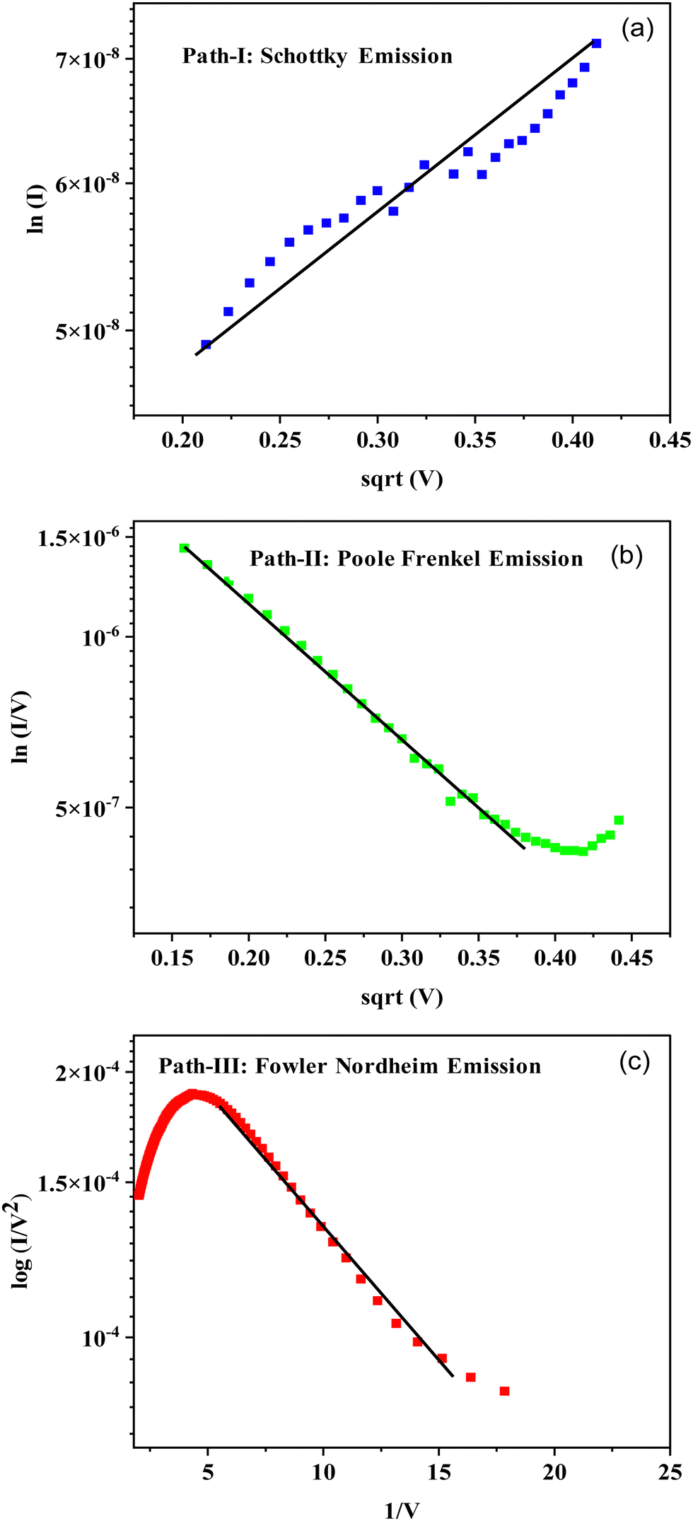 | ||
| Fig. 9 The experimental data of the Cu/Cu2S/DNA/Au junction fitted to various charge-transport mechanisms: (a) Schottky-barrier emission, (b) Poole–Frenkel emission and (c) direct Fowler–Nordheim tunneling. The solid lines show the best fit to the experimental data points. | ||
4. Conclusions
In summary, a simple room-temperature technique has been proposed to form multiple interfaces of Cu2S and DNA on a copper substrate as memristors. A hexagonal structure of Cu2S is obtained, which has been confirmed by XRD and SEM measurements. Worm-like DNA structures have been deposited over the hexagonal-Cu2S film via an electrochemical method. The Cu–Cu2S–DNA–Au junctions have been characterized for memristor behavior and these devices exhibit threshold electrical switching with a good ON/OFF ratio of 102 and a good endurance, which has been tested for a large number of cycles. This unique behavior of the present junctions has been explained in terms of their energy-band diagram. The proposed interfaces are simple, low cost and easily scalable for commercial applications.Conflicts of interest
There are no conflicts to declare.Acknowledgements
One of the authors, Miss Smita Gajanan Naik, is grateful for a DST-INSPIRE fellowship.References
- T. Shi, R. Wang, Z. Wu, Y. Sun, J. An and Q. Liu, A Review of Resistive Switching Devices: Performance Improvement, Characterization, and Applications, Small Struct., 2021, 2(4), 2000109, DOI:10.1002/sstr.202000109.
- Z. Wang, H. Wu, G. W. Burr, C. S. Hwang, K. L. Wang, Q. Xia and J. J. Yang, Resistive Switching Materials for Information Processing, Nat. Rev. Mater., 2020, 5(3), 173–195, DOI:10.1038/s41578-019-0159-3.
- S. Slesazeck and T. Mikolajick, Nanoscale Resistive Switching Memory Devices: A Review, Nanotechnology, 2019, 30(35), 352003, DOI:10.1088/1361-6528/ab2084.
- M. N. Almadhoun, M. Speckbacher, B. C. Olsen, E. J. Luber, S. Y. Sayed, M. Tornow and J. M. Buriak, Bipolar Resistive Switching in Junctions of Gallium Oxide and P-Type Silicon, Nano Lett., 2021, 21(6), 2666–2674, DOI:10.1021/acs.nanolett.1c00539.
- S. G. Naik and M. H. K. Rabinal, Compositional Tuning of Negative Differential Resistance in a Bulk Silver Iodide Memristor, New J. Chem., 2021, 45(3), 1667–1676, 10.1039/d0nj05427e.
- C. Pan, Y. Ji, N. Xiao, F. Hui, K. Tang, Y. Guo, X. Xie, F. M. Puglisi, L. Larcher, E. Miranda, L. Jiang, Y. Shi, I. Valov, P. C. McIntyre, R. Waser and M. Lanza, Coexistence of Grain-Boundaries-Assisted Bipolar and Threshold Resistive Switching in Multilayer Hexagonal Boron Nitride, Adv. Funct. Mater., 2017, 27(10), 1604811, DOI:10.1002/adfm.201604811.
- T. W. Hickmott, Low-Frequency Negative Resistance in Thin Anodic Oxide Films, J. Appl. Phys., 1962, 33(9), 2669–2682, DOI:10.1063/1.1702530.
- Y. Qiao, T. Hirtz, F. Wu, G. Deng, X. Li, Y. Zhi, H. Tian, Y. Yang and T. L. Ren, Fabricating Molybdenum Disulfide Memristors, ACS Appl. Electron. Mater., 2020, 2(2), 346–370, DOI:10.1021/acsaelm.9b00655.
- L. Yin, R. Cheng, Y. Wen, C. Liu and J. He, Emerging 2D Memory Devices for In-Memory Computing, Adv. Mater., 2021, 33(29), 2007081, DOI:10.1002/adma.202007081.
- L. Li and D. Wen, Memory Behavior of Multi-Bit Resistive Switching Based on Multiwalled Carbon Nanotubes, Org. Electron., 2016, 34, 12–17, DOI:10.1016/j.orgel.2016.03.041.
- C. E. Cava, C. Persson, A. J. G. Zarbin and L. S. Roman, Resistive Switching in Iron-Oxide-Filled Carbon Nanotubes, Nanoscale, 2014, 6(1), 378–384, 10.1039/c3nr04320g.
- J. M. Yang, E. S. Choi, S. Y. Kim, J. H. Kim, J. H. Park and N. G. Park, Perovskite-Related (CH3NH3)3Sb2Br9 for Forming-Free Memristor and Low-Energy-Consuming Neuromorphic Computing, Nanoscale, 2019, 11(13), 6453–6461, 10.1039/c8nr09918a.
- Z. Liu, P. Cheng, Y. Li, R. Kang, Z. Zhang, Z. Zuo and J. Zhao, High Temperature CsPbBrxI3- XMemristors Based on Hybrid Electrical and Optical Resistive Switching Effects, ACS Appl. Mater. Interfaces, 2021, 13(49), 58885–58897, DOI:10.1021/acsami.1c13561.
- B. Hwang and J. S. Lee, Lead-Free, Air-Stable Hybrid Organic-Inorganic Perovskite Resistive Switching Memory with Ultrafast Switching and Multilevel Data Storage, Nanoscale, 2018, 10(18), 8578–8584, 10.1039/c8nr00863a.
- Y. Wang, Z. Lv, L. Zhou, X. Chen, J. Chen, Y. Zhou, V. A. L. Roy and S. T. Han, Emerging Perovskite Materials for High Density Data Storage and Artificial Synapses, J. Mater. Chem. C, 2018, 6(7), 1600–1617, 10.1039/c7tc05326f.
- Z. Wang, M. Yin, T. Zhang, Y. Cai, Y. Wang, Y. Yang and R. Huang, Engineering Incremental Resistive Switching in TaO: X Based Memristors for Brain-Inspired Computing, Nanoscale, 2016, 8(29), 14015–14022, 10.1039/c6nr00476h.
- W. Lu, L. M. Wong, S. Wang and K. Zeng, Probing Electrochemically Induced Resistive Switching of TiO2 Using SPM Techniques, Phys. Chem. Chem. Phys., 2017, 19(46), 31399–31409, 10.1039/c7cp06992h.
- B. Sun, Y. Liu, W. Zhao and P. Chen, Magnetic-Field and White-Light Controlled Resistive Switching Behaviors in Ag/[BiFeO3/γ-Fe2O3]/FTO Device, RSC Adv., 2015, 5(18), 13513–13518, 10.1039/c4ra14605k.
- K. Zhu, X. Liang, B. Yuan, M. A. Villena, C. Wen, T. Wang, S. Chen, F. Hui, Y. Shi and M. Lanza, Graphene-Boron Nitride-Graphene Cross-Point Memristors with Three Stable Resistive States, ACS Appl. Mater. Interfaces, 2019, 11(41), 37999–38005, DOI:10.1021/acsami.9b04412.
- Z. Fan, H. Fan, L. Yang, P. Li, Z. Lu, G. Tian, Z. Huang, Z. Li, J. Yao, Q. Luo, C. Chen, D. Chen, Z. Yan, M. Zeng, X. Lu, X. Gao and J. M. Liu, Resistive Switching Induced by Charge Trapping/Detrapping: A Unified Mechanism for Colossal Electroresistance in Certain Nb:SrTiO3-Based Heterojunctions, J. Mater. Chem. C, 2017, 5(29), 7317–7327, 10.1039/c7tc02197f.
- X. Zhu, C. Du, Y. Jeong and W. D. Lu, Emulation of Synaptic Metaplasticity in Memristors, Nanoscale, 2017, 9(1), 45–51, 10.1039/c6nr08024c.
- S. Gao, X. Yi, J. Shang, G. Liu and R. W. Li, Organic and Hybrid Resistive Switching Materials and Devices, Chem. Soc. Rev., 2019, 48(6), 1531–1565, 10.1039/c8cs00614h.
- A. Adeyemo, A. Jabir, J. Mathew, E. Martinelli, C. Di Natale and M. Ottavi, Reliable Gas Sensing with Memristive Array, 2017 IEEE 23rd Int. Symp. On-Line Test. Robust Syst. Des. IOLTS 2017, 2017, No. 1, pp. 244–246 DOI:10.1109/IOLTS.2017.8046228.
- M. Vidiš, T. Plecenik, M. Moško, S. Tomašec, T. Roch, L. Satrapinskyy, B. Grančič and A. Plecenik, Gasistor: A Memristor Based Gas-Triggered Switch and Gas Sensor with Memory, Appl. Phys. Lett., 2019, 115(9), 093504, DOI:10.1063/1.5099685.
- S. Kumar, G. Meng, P. Mishra, N. Tripathi and A. Bannov, A systematic review on 2D MoS2 for nitrogen dioxide (NO2) sensing at room temperature, Mater. Today Commun., 2023, 34, 105045, DOI:10.1016/j.mtcomm.2022.105045.
- P. Qiu, Y. Qin and Q. Xia, Ultrasensitive memristor-based gas sensor (gasistor) with gas-triggered switch and memory function for dilute NH3 detection, Sens. Actuators, B, 2022, 373, 132730, DOI:10.1016/j.snb.2022.132730.
- W. Wang, G. Zhou, Y. Wang, B. Sun, M. Zhou, C. Fang, C. Xu, J. Dong, F. Wang, S. Duan and Q. Song, An Analogue Memristor Made of Silk Fibroin Polymer, J. Mater. Chem. C, 2021, 9(41), 14583–14588, 10.1039/d1tc03315h.
- K. J. Tomek, K. Volkel, A. Simpson, A. G. Hass, E. W. Indermaur, J. M. Tuck and A. J. Keung, Driving the Scalability of DNA-Based Information Storage Systems, ACS Synth. Biol., 2019, 8(6), 1241–1248, DOI:10.1021/acssynbio.9b00100.
- D. Panda, K. A. Molla, M. J. Baig, A. Swain, D. Behera and M. Dash, DNA as a Digital Information Storage Device: Hope or Hype?, 3 Biotech, 2018, 8(5), 239, DOI:10.1007/s13205-018-1246-7.
- M. Taniguchi and T. Kawai, DNA Electronics, Phys. E, 2006, 33(1), 1–12, DOI:10.1016/j.physe.2006.01.005.
- H. Tabata, L. T. Cai, J. H. Gu, S. Tanaka, Y. Otsuka, Y. Sacho, M. Taniguchi and T. Kawai, Toward the DNA Electronics, Synth. Met., 2003, 133–134, 469–472, DOI:10.1016/S0379-6779(02)00386-7.
- L. Ceze, J. Nivala and K. Strauss, Molecular Digital Data Storage Using DNA, Nat. Rev. Genet., 2019, 20(8), 456–466, DOI:10.1038/s41576-019-0125-3.
- N. Rizan, C. Y. Yew, M. R. Niknam, J. Krishnasamy, S. Bhassu, G. Z. Hong, S. Devadas, M. S. M. Din, H. A. Tajuddin, R. Y. Othman, S. M. Phang, M. Iwamoto and V. Periasamy, Electronic Properties of Synthetic Shrimp Pathogens-Derived DNA Schottky Diodes, Sci. Rep., 2018, 8(1), 896, DOI:10.1038/s41598-017-18825-6.
- V. Periasamy, N. Rizan, H. M. J. Al-Ta’Ii, Y. S. Tan, H. A. Tajuddin and M. Iwamoto, Measuring the Electronic Properties of DNA-Specific Schottky Diodes Towards Detecting and Identifying Basidiomycetes DNA, Sci. Rep., 2016, 6, 29879, DOI:10.1038/srep29879.
- S. Bera, A. K. Katiyar, A. K. Sinha, S. P. Mondal and S. K. Ray, Resistive Switching Characteristics of a Single Zn-Doped CuS Nanoball Anchored with Multi-Walled Carbon Nanotubes, Mater. Des., 2016, 101, 197–203, DOI:10.1016/j.matdes.2016.03.160.
- K. Mallick, V. K. Perla and S. K. Ghosh, Carbon Nitride Supported Ultrafine Manganese Sulfide Based Nonvolatile Resistive Switching Device for Nibble-Sized Memory Application, ACS Appl. Electron. Mater., 2020, 2(12), 3987–3993, DOI:10.1021/acsaelm.0c00817.
- J. Yoon, M. Mohammadniaei, H. K. Choi, M. Shin, G. B. Bapurao, T. Lee and J. W. Choi, Resistive Switching Biodevice Composed of MoS2-DNA Heterolayer on the Gold Electrode, Appl. Surf. Sci., 2019, 478, 134–141, DOI:10.1016/j.apsusc.2019.01.229.
- R. Mulla and M. K. Rabinal, Large-Scale Synthesis of Copper Sulfide by Using Elemental Sources via Simple Chemical Route, Ultrason. Sonochem., 2017, 39, 528–533, DOI:10.1016/j.ultsonch.2017.05.027.
- B. K. Murgunde, M. K. Rabinal and M. N. Kalasad, Biologically Active Nanocomposite of DNA-PbS Nanoparticles: A New material for non-volatile memory devices, Appl. Surf. Sci., 2018, 427, 344–353, DOI:10.1016/j.apsusc.2017.08.001.
- S. G. Naik and M. H. K. Rabinal, Significance of Electrode Contact Area on Memristive Parameters of Silver Iodide, Mater. Sci. Semicond. Process., 2022, 138, 106309, DOI:10.1016/j.mssp.2021.106309.
- C. Guo, K. Wang, E. Zerah-Harush, J. Hamill, B. Wang, Y. Dubi and B. Xu, Molecular Rectifier Composed of DNA with High Rectification Ratio Enabled by Intercalation, Nat. Chem., 2016, 8(5), 484–490, DOI:10.1038/nchem.2480.
- Y. C. Chang, C. J. Lee, L. W. Wang and Y. H. Wang, Air-Stable Gelatin Composite Memory Devices on a Paper Substrate, Org. Electron., 2019, 65, 77–81, DOI:10.1016/j.orgel.2018.11.012.
- J. Park and S. Kim, Improving Endurance and Reliability by Optimizing the Alternating Voltage in Pt/ZnO/TiN RRAM, Results Phys., 2022, 39, 105731, DOI:10.1016/j.rinp.2022.105731.
- J. Choi and S. Kim, Coexistence of Long-Term Memory and Short-Term Memory in an SiNx-Based Memristor, Phys. Status Solidi RRL, 2020, 14, 2000357, DOI:10.1002/pssr.202000357.
- R. Du and G. Pourtois, Fundamentals of Low-Resistive 2D-Semiconductor Metal Contacts: An Ab-Initio NEGF Study, npj 2D Mater. Appl., 2023, 7, 38, DOI:10.1038/s41699-023-00402-3.
- J. H. Kim, J. H. Hwang, J. Suh, S. Tongay, S. Kwon, C. C. Hwang, J. Wu and J. Young Park, Work Function Engineering of Single Layer Graphene by Irradiation-Induced Defects, Appl. Phys. Lett., 2013, 103(17), 171604, DOI:10.1063/1.4826642.
- J. S. Kim, B. Lägel, E. Moons, N. Johansson, I. D. Baikie, W. R. Salaneck, R. H. Friend and F. Cacialli, Kelvin probe and ultraviolet photoemission measurements of indium tin oxide work function: a comparison, Synth. Met., 2000, 111–112, 311–314 CrossRef CAS.
- V. K. Perla, S. K. Ghosh and K. Mallick, Transport Mechanism of Copper Sulfide Embedded Carbon Nitride Thin Films: A Formation Free Memristor, Mater. Adv., 2020, 1(2), 228–234, 10.1039/d0ma00062k.
- G. Dagan, T. F. Ciszek and D. Cahen, Ion Migration in Chalcopyrite Semiconductors, J. Phys. Chem., 1992, 96(26), 11009–11017, DOI:10.1021/j100205a073.
- F. C. Collins and T. Nakayama, Transport Processes in the Thermal Growth of Metal and Semiconductor Oxide Films, J. Electrochem. Soc., 1967, 114(2), 167, DOI:10.1149/1.2426531.
- M. Venkateswarlu and N. Satyanarayana, AC Conductivity Studies of Silver Based Fast Ion Conducting Glassy Materials for Solid State Batteries, Mater. Sci. Eng., B, 1998, 54(3), 189–195, DOI:10.1016/s0921-5107(98)00156-1.
- Y. Zhou, L. Tang, G. Zeng, C. Zhang, Y. Zhang and X. Xie, Current Progress in Biosensors for Heavy Metal Ions Based on DNAzymes/DNA Molecules Functionalized Nanostructures: A Review, Sens. Actuators, B, 2016, 223, 280–294, DOI:10.1016/j.snb.2015.09.090.
Footnote |
| † Electronic supplementary information (ESI) available. See DOI: https://doi.org/10.1039/d3ma00080j |
| This journal is © The Royal Society of Chemistry 2023 |