
 Open Access Article
 This Open Access Article is licensed under a
 Creative Commons Attribution 3.0 Unported Licence
The electronic and interfacial properties of a vdW heterostructure composed of penta-PdSe2 and biphenylene monolayers
Muhammad Azhar
Nazir
,
Yiheng
Shen
,
Arzoo
Hassan
 and
Qian
Wang
*
and
Qian
Wang
*
School of Materials Science and Engineering, Peking University, Beijing 100871, China. E-mail: qianwang2@pku.edu.cn
First published on 28th February 2023
Abstract
It is of current interest to develop van der Waals (vdW) heterostructures with tunable electronic properties for technical applications. Motivated by the synthesis of a metallic carbon nanosheet termed the biphenylene network (BPN) [Q. Fan, L. Yan, M. W. Tripp, O. Krejčí, S. Dimosthenous, S. R. Kachel, M. Chen, A. S. Foster, U. Koert, P. Liljeroth et al., Science, 2021, 372, 852–856] and semiconducting penta-PdSe2 sheets [A. D. Oyedele, S. Yang, L. Liang, A. A. Puretzky, K. Wang, J. Zhang, P. Yu, P. R. Pudasaini, A. W. Ghosh, Z. Liu et al., J. Am. Chem. Soc., 2017, 139, 14090–14097], we rationally design a vdW heterostructure by vertically stacking these two individual sheets. The state-of-the-art first-principles calculations show that the penta-PdSe2 sheet well preserves its intrinsic properties when forming a vdW contact with BPN. The heterostructure possesses an n-type Schottky contact with a Schottky barrier of 0.54 eV, and a negative band-bending of 0.56 eV at the lateral interface with electrons as major transport carriers. These features make the penta-PdSe2/BPN heterojunction promising for applications in field-effect transistors.
1. Introduction
The assembly of different two-dimensional (2D) materials into vertically stacked van der Waals (vdW) heterostructures has fueled a novel concept of designing and synthesizing new materials with improved functionalities distinct from those of each component.1–3 Unlike traditional heterostructures, which strongly rely on direct covalent bonding and strict lattice-matching conditions,4 the weak vdW interaction and the absence of covalent bonding between the two components allow the construction of an artificial interface that offers a great degree of freedom for interlayer engineering. More importantly, the absence of dangling bonds endows 2D materials with great potential and excellent stacking stability to construct vdW heterostructures in an arbitrary sequence.5 Since the discovery of graphene,6 significant efforts have been devoted to the design of vdW heterostructures by stacking various 2D sheets, including graphene,7,8 penta-graphene,9,10 graphitic carbon nitride,11,12 transition metal–carbides,13,14 and boron nitrides,15,16 for their potential applications in the fields like energy storage,17–19 photocatalysis,20,21 and optoelectronic devices.22–24 It is also worth mentioning that extensive research is still underway to design and synthesize vdW heterostructures with desired properties under various conditions.In parallel to the design and synthesis of new heterostructures constructed using hexagonal building blocks, geometrically assembled vdW heterostructures have become the major research hotspot for realizing more controllable devices. Considering the structure–property relationship, one can expect that vdW heterostructures composed of layers with different geometrical configurations would exhibit different properties. In this regard, pentagonal materials have initiated a new era in materials with the prediction of penta-graphene25,26 and the synthesis of penta-PdSe2,27 penta-NiN2,28 and penta-Si nanoribbons29 as practical templates to construct pentagon-based vdW heterostructures. Additionally, their uniqueness in device functions strongly depends on their underlying electronic structures and pentagonal stacking patterns to tune the structure–property relationship. Among these, the PdSe2 sheet has attracted increasing research interest due to its excellent performance in electronics. For example, a high electron field-effect mobility of ∼158 cm2 V−1 s−1 in few-layer PdSe2 extends its credibility in field-effect transistors (FETs).27 From the device's perspective, a large rectification ratio of up to 6.3 × 10⁵ for PdSe2/MoTe2,30 5.5 × 10⁵ for PdSe2/GeSe,31 a high photoresponsivity of 58.8 A W−1 (at 1650 nm) for PdSe2/InSe,32 6.9 A W−1 for PdSe2/MoS2,33 a high specific detectivity of 5.29 × 10¹¹ Jones for PdSe2/MoSe234 and significant broadband image sensing for PdSe2/MoTe2,35 PdSe2/WS236 vdW heterostructures extend the contact realization of PdSe2 sheets under applied conditions. In addition to the experimental results, Hassan et al.37 and Li et al.38 investigated the interfacial properties of PdSe2-graphene and PdSe2-metal contacts under different conditions. These advances clearly show that the penta-PdSe2 sheet can flexibly form heterojunctions with other 2D materials.
Recently, Fan et al.39 synthesized an ultra-flat metallic carbon sheet, namely the biphenylene network (BPN), which is composed of tetra-, hexa-, and octa-gonal rings and features pure sp2-hybridization. By using first-principles calculations, some theoretical studies have also confirmed metallicity,40 magnetic and topological ordering,41 anisotropic charge transport,42 and remarkable negative thermal expansion43 in the BPN monolayer, which extend the functionality of this sheet for advanced nanodevices. From the perspective of heterojunctions, it would be interesting to explore how the BPN sheet interacts with penta-PdSe2 to form a heterostructure.
In this work, we report the first study on the electronic and interfacial properties of a 2D vdW heterostructure composed of vertically stacked penta-PdSe2 and BPN monolayers. We demonstrate that the heterostructure exhibits an n-type Schottky contact feature as well as negative band-bending at the lateral interface of the heterojunction, suggesting that the PdSe2/BPN heterostructure is promising for FET devices.
2. Computational details
All the calculations are performed within the framework of density functional theory (DFT) implemented in Vienna ab initio Simulation Package (VASP).44,45 The projector-augmented-wave (PAW) method is used to describe the interactions between valence electrons and ion cores.46 The generalized gradient approximation (GGA)47 based Perdew–Burke–Ernzerhof (PBE) functional is used to treat the electronic exchange–correlation interactions of electrons.46 In addition, the DFT-D3 functional48,49 is considered for all the calculations to describe the effect of vdW interactions in the PdSe2/BPN heterostructure. The valence electronic configurations of 5s14d9, 4s24p4, and 2s22p2 are taken for Pd, Se, and C atoms, respectively. The kinetic energy cut-off of 520 eV is used to expand the wave functions and pseudo-atomic calculations. A vacuum space of 25 Å along the z-direction (perpendicular to the PdSe2/BPN heterojunction layers) separates the contact regions to prevent interactions between the periodic images. The first Brillouin zone (BZ) is sampled with a fine grid of 9 × 2 × 1. The atomic positions are fully relaxed with an energy convergence threshold of 10−4 eV and a force convergence threshold of 0.01 eV Å−1. Ab initio molecular dynamics (AIMD) simulations are performed under the canonical ensemble, and the temperature fluctuation is controlled by the Nosé–Hoover thermostat.503. Results and discussion
3.1. Structure and electronic properties of free-standing PdSe2 and BPN monolayers
Before focusing on the PdSe2/BPN heterojunction, we first discuss the geometric structure and electronic properties of the free-standing PdSe2 and BPN monolayers, as shown in Fig. 1. The lattice of the penta-PdSe2 monolayer belongs to the monoclinic P21/C symmetry (space group no. 14), with the optimized lattice constants of a = 5.75 Å and b = 5.92 Å, whereas the BPN layer possesses an orthorhombic Pmma symmetry (space group no. 47), with the optimized constants of a = 3.76 Å and b = 4.52 Å. Studies reveal that both individual sheets well preserve their environmental potential by offering dynamical, thermal and mechanical stability under applied conditions.27,39,40,51 The electronic band structures illustrate that penta-PdSe2 is semiconducting with an indirect band gap of 1.36 eV, while the BPN monolayer is metallic because the partially filled energy bands cross the Fermi level. Furthermore, the partial density of states (PDOS) of the PdSe2 sheet shows that the valence band maximum (VBM) and conduction band minimum (CBM) are mainly contributed by the Pd-4d and Se-4p orbitals.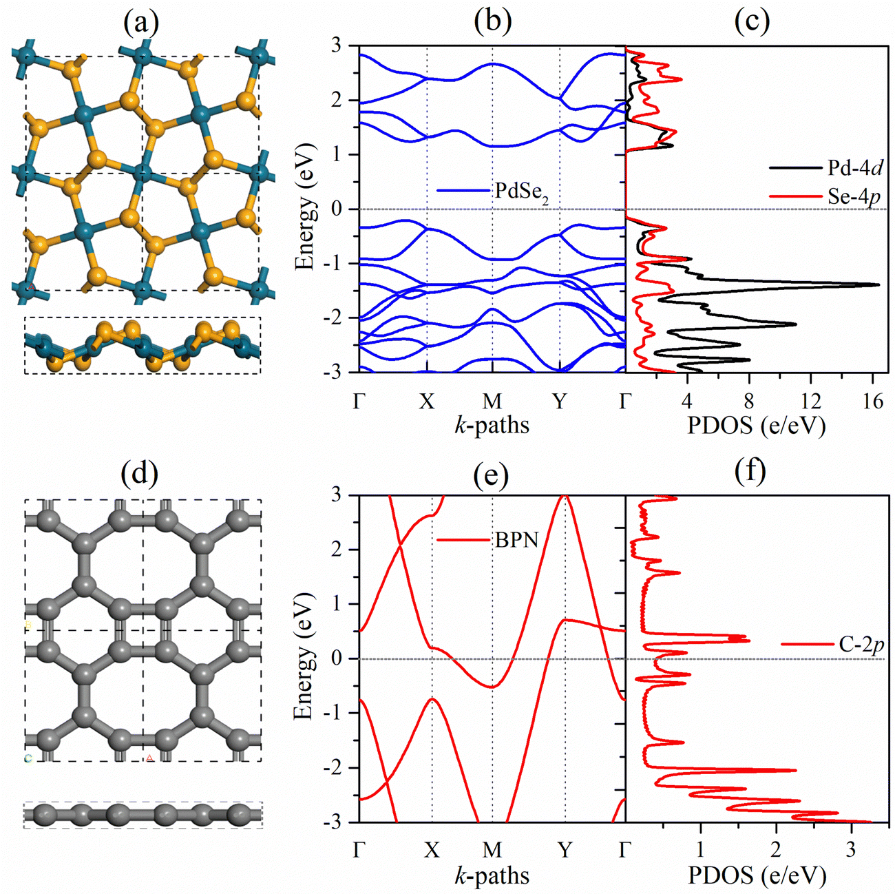 | ||
| Fig. 1 Top and side views of 2 × 2, electronic band structure, and the corresponding PDOS of the free-standing (a)–(c) penta-PdSe2, and (d)–(f) BPN monolayer. The Fermi energy (EF) is set to 0 eV. The cyan, yellow, and grey spheres represent Pd, Se, and C atoms, respectively. | ||
3.2. Structure and stability of the PdSe2/BPN heterostructure
We design the PdSe2/BPN heterostructure by vertically stacking the two monolayers. Unlike the heterostructures purely composed of hexagonal building blocks,15,52–55 the PdSe2/BPN heterojunction comprises mixed geometric blocks such as tetra-hexa and octagonal blocks of C as well as purely pentagonal blocks composed of Pd and Se atoms. Due to the different lattice symmetries and lattice parameters, special attention is devoted to control the lattice mismatch between the penta-PdSe2 and BPN layers in order to do calculations using periodic boundary conditions. In this respect, we used a cell-matching code56 to construct PdSe2/BPN supercells, which are very suitable for making a vdW interface between two 2D sheets with different lattice constants and symmetrical images by controlling a minimal strain in the stacked supercell. Particularly, in this method, one sheet is placed on the other, and the most suitable shape of the stacked supercell is calculated by rotating that sheet by an angle ranging from 0 to 90° with a step difference of 1°. For PdSe2/BPN, we found the best match of the stacked configurations at 38° with the minimum number of atoms (60 C atoms, 20 Se atoms, and 10 Pd atoms) and the lattice mismatch threshold of 1%, as shown in Fig. 2(a). To save the computational cost, this configuration is considered for further investigations.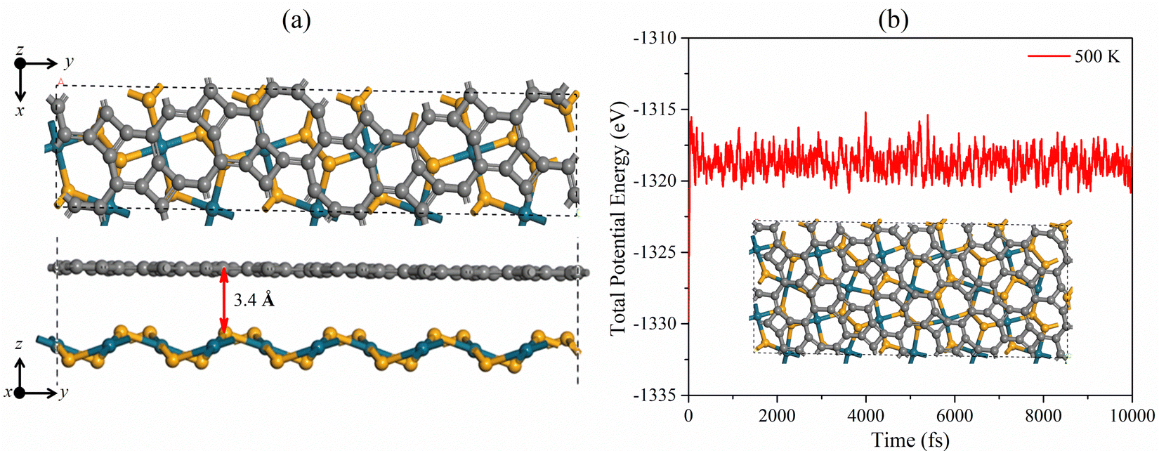 | ||
| Fig. 2 (a) Top and side views of 1 × 1, and (b) total potential energy fluctuation of the PdSe2/BPN heterostructure at 500 K. | ||
The optimized distance between the vertically stacked PdSe2 and BPN layers is 3.40 Å. To examine the interface stability of this system, we calculate its binding energy Eb with the following equation Eb = −[(EH − Ex − Ey)/A], where EH is the total energy of the PdSe2/BPN heterostructure, Ex and Ey are the total energies of the free-standing penta-PdSe2 and BPN monolayers, respectively, and A is the total area of the supercell of the heterostructure. The calculated binding energy Eb is 0.06 eV Å−2. The values of interlayer distance d and binding energy are comparable with those of the typical vdW crystals such as graphite [Eb = 0.28 J m−2 (0.0175 eV Å−2) and d = 3.60 Å]57 and hexagonal BN (Eb = 0.04 eV Å−2 and d = 3.30 Å),58 and some recently reported vdW heterostructures such as PdSe2/graphene (Eb = 0.02 eV Å−2 and d = 3.60 Å),37 implying that the PdSe2/BPN heterostructure can be classified based on the category of vdW type.
Furthermore, the thermal stability of the PdSe2/BPN system is investigated at 500 K with an AIMD simulation. The fluctuation of the total potential energy during a simulation time of 10 picoseconds (ps) with a time step of 1 femtosecond (fs) is plotted in Fig. 2(b). One can see that after 10![[thin space (1/6-em)]](https://www.rsc.org/images/entities/char_2009.gif) 000 steps, there is still no significant geometric distortion, and the energy of this system vibrates around a constant, confirming that the PdSe2/BPN heterostructure is thermally stable at 500 K.
000 steps, there is still no significant geometric distortion, and the energy of this system vibrates around a constant, confirming that the PdSe2/BPN heterostructure is thermally stable at 500 K.
3.3. Interfacial properties of the PdSe2/BPN heterostructure
The vdW interactions between the stacked monolayers can provide more freedom to engineer the carrier injections from a highly conductive electrode to a semiconductor channel for designing high-performance electronic devices. In order to analyze the electronic properties of the PdSe2/BPN system, we calculate the electronic band structure of the heterostructure and its projection on the PdSe2 and BPN sheets. As shown in Fig. 3(a) and (b), the electronic structures of both PdSe2 and BPN monolayers are well preserved, further confirming that the PdSe2/BPN system is a vdW heterostructure. In addition, as shown in Fig. 3(c), the DOS of the PdSe2/BPN heterojunction around the Fermi level is mainly contributed by the BPN sheet.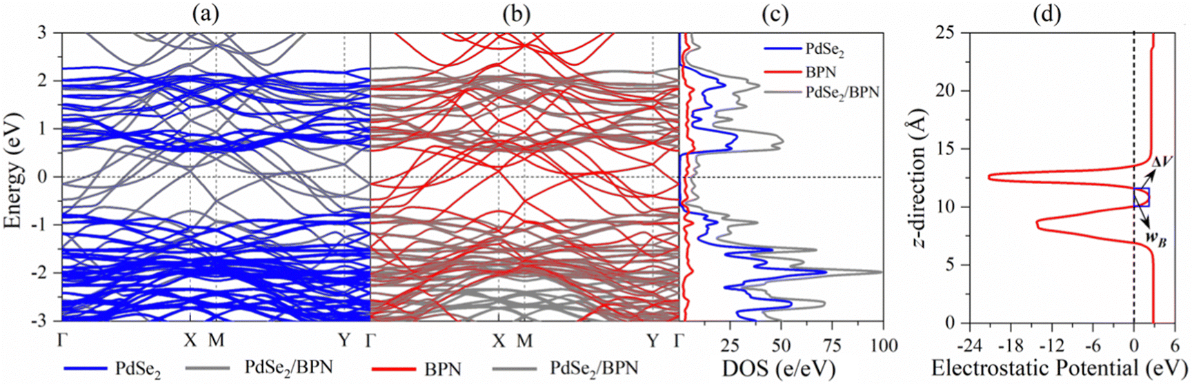 | ||
| Fig. 3 Projected band structures of (a) PdSe2 and (b) BPN monolayers where the grey lines represent the band structure of the PdSe2/BPN heterostructure. (c) DOS of penta-PdSe2, BPN, and the PdSe2/BPN heterostructure. (d) Electrostatic potential profile of the PdSe2/BPN heterostructure along the z-direction. The rectangular blue box represents the tunneling barrier, where ΔV and wB are the tunneling barrier height and width, respectively. | ||
We further explore the device performance of the PdSe2/BPN-based FET. As shown in the schematic in Fig. 4, the movement of charge carriers from the metallic electrode to the semiconducting channel needs to overcome three types of barriers, including the tunneling barrier, Schottky barrier (ΦV), and lateral barrier (ΦL). Among them, the tunneling barrier appears at the vertical interface B between the PdSe2 and BPN sheets because of the quantum features of the carriers, which strongly depends on the interface between the metal and the semiconductor. The Schottky barrier also appears at the vertical interface B. The magnitude of the Schottky barrier between an electrode and channel materials mainly depends on the nature of the electrode material, work function, and contact resistance. Additionally, the lateral barrier exists at the lateral interface D between the heterostructure and the channel and can be estimated by the band bending (ΔEF) values.
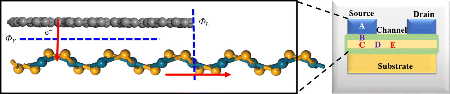 | ||
| Fig. 4 A typical illustration of the FET three regions (A), (C), and (E) with two interfaces (B) and (D). Movement of the charge carriers from the metallic electrode BPN to the semiconducting penta-PdSe2 channel, where ΦV and ΦL represent the Schottky barrier and lateral barrier, respectively. | ||
First, we evaluate the tunneling possibility (TP) of the PdSe2/BPN system from the tunneling barrier in the electrostatic potential profile, which is marked by the blue rectangle in Fig. 3(d), based on the Wentzel–Kramer–Brillouin (WKB) approximation,37
 | (1) |
| Structure | d | E b | ΔV | w B | TP | W H | Φ e | Φ h | ΔEF |
|---|---|---|---|---|---|---|---|---|---|
| PdSe2/BPN | 3.4 | 0.06 | 1.5 | 2.3 | 60 | 4.64 | 0.54 | 0.80 | −0.56 |
| PdSe2/graphene37 | 3.6 | 0.02 | 3.8 | — | — | — | 0.22 | — | −0.94 |
| PdSe2/Ag37 | 2.9 | 0.38 | 4.0 | 17.7 | 40 | 4.43 | 0.87 | 0.56 | 0.05 |
| PdSe2/Au37 | 2.9 | 0.44 | 3.2 | 10.4 | 18 | 5.24 | 0.62 | 0.81 | 0.03 |
| PdSe2/Cu37 | 2.5 | 0.57 | 0.0 | 0.0 | 100 | 4.49 | 0.79 | 0.64 | −0.51 |
| PdSe2/Ti37 | 2.5 | 1.34 | 0.0 | 0.0 | 100 | 5.20 | 0.58 | 0.85 | −0.14 |
| PdSe2/Pb37 | 3.1 | 0.31 | 2.4 | 9.2 | 9.2 | 4.11 | 0.76 | 0.67 | 0.41 |
| PdSe2/Sc38 | 2.1 | — | — | — | — | 3.5 | — | — | — |
| PdSe2/Al38 | 2.3 | — | — | — | — | 4.3 | 0.12 | — | — |
| PdSe2/MoTe238 | 3.2 | — | — | — | — | 5.19 | — | — | — |
Next, we calculate the Schottky barrier of the PdSe2/BPN heterostructure, which is among the most important parameters to determine the contact resistance in a FET device. Following the Schottky–Mott rule,37 the Schottky barrier height (SBH) of electrons (Φe) and holes (Φh) is defined as the energy difference between the Fermi level and the respective energy band edges of the semiconductor,
| Φe = ECBM − EF, Φh = EF − EVBM | (2) |
In addition, to estimate the lateral barrier, we study the band bending in PdSe2/BPN heterostructures in the scheme of the current-in-plane (CIP)9 model. As shown in Fig. 5, the CIP model is mainly divided into three parts: the left side for the PdSe2/BPN heterojunction, the middle one for the interface between the heterojunction and the free-standing monolayer, and the right side for the free-standing PdSe2 layer. The energy levels for the heterojunction and the free-standing PdSe2 layer are aligned to the vacuum energy (Evac). The work functions of the PdSe2/BPN heterojunction and the free-standing PdSe2 monolayer are calculated to be WH = 4.64 eV and WPdSe2 = 5.20 eV, respectively. As listed in Table 1, the band bending ΔEF at the lateral interface D is estimated by ΔEF = WH − WPdSe2 = −0.56 eV, which is quite comparable to the vdW contacts such as PdSe2/graphene and PdSe2/Ti with ΔEF = −0.94 and −0.14 eV, respectively.37 The negative band bending (ΔEF < 0) confirms that an n-type channel is formed between the PdSe2/BPN heterostructure and the free-standing PdSe2 sheet, as reported in PdSe2/graphene37 and PdSe2/Al contacts.38
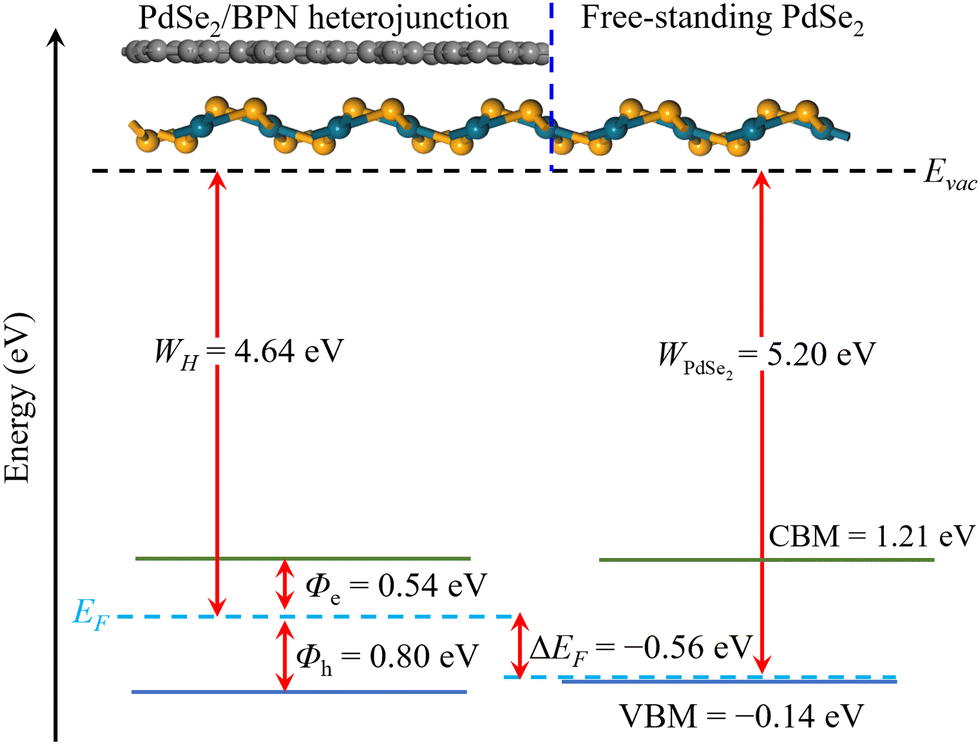 | ||
| Fig. 5 Schematic diagram of the CIP model and band alignment in the PdSe2/BPN heterojunction. Evac is the vacuum level to align all the values, and WH and WPdSe2 are the work functions of the PdSe2/BPN heterostructure and free-standing PdSe2 monolayer. The blue, black, and cyan dashed lines represent the interface between the electrode and channel regions, vacuum level, and the Fermi energy, respectively. The green and blue solid lines indicate the CBM and VBM values. | ||
Due to its relatively high TP and low SBH, the contact between PdSe2 and BPN could be among the most suitable design for PdSe2-based FET applications.
4. Conclusions
In this work, we report a vdW heterostructure composed of purely pentagonal PdSe2 and atomically flat carbon allotrope BPN, which serve as the channel and electrode materials, respectively, because of their intrinsic semiconducting and metallic features. The energetic and thermal stabilities of this heterostructure are confirmed by the binding energy calculations and AIMD simulations. The heterostructure possesses an n-type Schottky contact and negative band-bending at the lateral interface with electrons as major transport carriers. Compared to the vdW heterostructure of penta-PdSe2/graphene, the penta-PdSe2/BPN heterojunction has a lower tunneling barrier height due to the co-existence of 4- and 8-rings in the BPN sheet, leading to a high tunneling possibility of ∼60% at the junction. Together with the synthesis of PdSe2 and BPN sheets, these findings would trigger more explorations for the PdSe2/BPN heterostructure in future device applications.Conflicts of interest
The authors declare that they have no competing financial interests or personal relationships that could have appeared to influence the work reported in this paper.Acknowledgements
This work is partially supported by grants from the National Natural Science Foundation of China (Grant no. NSFC-11974028 and NSFC-12274007) and the National Key Research and Development Program of the Ministry of Science and Technology of the People's Republic of China (2017YFA0205003). This work is also supported by the high-performance computing platform of Peking University, China.References
- W. Liao, Y. Huang, H. Wang and H. Zhang, Appl. Mater. Today, 2019, 16, 435–455 CrossRef.
- K. Novoselov, A. Mishchenko, A. Carvalho and A. Castro Neto, Science, 2016, 353, aac9439 CrossRef CAS PubMed.
- A. K. Geim and I. V. Grigorieva, Nature, 2013, 499, 419–425 CrossRef CAS PubMed.
- P. Wang, C. Jia, Y. Huang and X. Duan, Matter, 2021, 4, 552–581 CrossRef CAS.
- Y. Wang, J. Pang, Q. Cheng, L. Han, Y. Li, X. Meng, B. Ibarlucea, H. Zhao, F. Yang and H. Liu, Nano-Micro Lett., 2021, 13, 1–52 CrossRef CAS PubMed.
- K. S. Novoselov, A. K. Geim, S. V. Morozov, D.-E. Jiang, Y. Zhang, S. V. Dubonos, I. V. Grigorieva and A. A. Firsov, Science, 2004, 306, 666–669 CrossRef CAS PubMed.
- Z. Zhang, P. Lin, Q. Liao, Z. Kang, H. Si and Y. Zhang, Adv. Mater., 2019, 31, 1806411 CrossRef PubMed.
- X. Wu, R. Yang, X. Chen and W. Liu, Nanomaterials, 2022, 12, 196 CrossRef CAS PubMed.
- Y. Guo, F. Q. Wang and Q. Wang, Appl. Phys. Lett., 2017, 111, 073503 CrossRef.
- A. Hassan, Y. Guo, Q. Wang, Y. Kawazoe and P. Jena, J. Appl. Phys., 2019, 125, 065308 CrossRef.
- G.-C. Guo, R.-Z. Wang, B.-M. Ming, C. Wang, S.-W. Luo, M. Zhang and H. Yan, J. Mater. Chem. A, 2019, 7, 2106–2113 RSC.
- J. Fu, J. Yu, C. Jiang and B. Cheng, Adv. Energy Mater., 2018, 8, 1701503 CrossRef.
- Z. Kou, T. Wang, Q. Gu, M. Xiong, L. Zheng, X. Li, Z. Pan, H. Chen, F. Verpoort and A. K. Cheetham, Adv. Energy Mater., 2019, 9, 1803768 CrossRef.
- J. Zhu, H. Wang, L. Ma and G. Zou, Nano Res., 2021, 14, 3416–3422 CrossRef CAS.
- X. Song, J. Sun, Y. Qi, T. Gao, Y. Zhang and Z. Liu, Adv. Energy Mater., 2016, 6, 1600541 CrossRef.
- S. Ullah, P. A. Denis, M. G. Menezes and F. Sato, Comput. Mater. Sci., 2021, 188, 110233 CrossRef CAS.
- D. K. Bediako, M. Rezaee, H. Yoo, D. T. Larson, S. Zhao, T. Taniguchi, K. Watanabe, T. L. Brower-Thomas, E. Kaxiras and P. Kim, Nature, 2018, 558, 425–429 CrossRef CAS PubMed.
- P. Das, Q. Fu, X. Bao and Z.-S. Wu, J. Mater. Chem. A, 2018, 6, 21747–21784 RSC.
- E. Pomerantseva and Y. Gogotsi, Nat. Energy, 2017, 2, 1–6 Search PubMed.
- Y.-L. Liu, Y. Shi, H. Yin and C.-L. Yang, Appl. Phys. Lett., 2020, 117, 063901 CrossRef CAS.
- K. Ren, J. Yu and W. Tang, J. Alloys Compd., 2020, 812, 152049 CrossRef CAS.
- J. Y. Lee, J.-H. Shin, G.-H. Lee and C.-H. Lee, Nanomaterials, 2016, 6, 193 CrossRef PubMed.
- A. Abid, M. Haneef, S. Ali and A. Dahshan, J. Phys. Chem. Solids, 2022, 161, 110433 CrossRef CAS.
- S. J. Liang, B. Cheng, X. Cui and F. Miao, Adv. Mater., 2020, 32, 1903800 CAS.
- S. Zhang, J. Zhou, Q. Wang, X. Chen, Y. Kawazoe and P. Jena, Proc. Natl. Acad. Sci. U. S. A., 2015, 112, 2372–2377 CrossRef CAS PubMed.
- M. A. Nazir, A. Hassan, Y. Shen and Q. Wang, Nano Today, 2022, 44, 101501 CrossRef CAS.
- A. D. Oyedele, S. Yang, L. Liang, A. A. Puretzky, K. Wang, J. Zhang, P. Yu, P. R. Pudasaini, A. W. Ghosh and Z. Liu, et al., J. Am. Chem. Soc., 2017, 139, 14090–14097 CrossRef CAS.
- M. Bykov, E. Bykova, A. V. Ponomareva, F. Tasnadi, S. Chariton, V. B. Prakapenka, K. Glazyrin, J. S. Smith, M. F. Mahmood and I. A. Abrikosov, ACS Nano, 2021, 15, 13539–13546 CrossRef CAS PubMed.
- J. I. Cerdá, J. Sławińska, G. Le Lay, A. C. Marele, J. M. Gómez-Rodríguez and M. E. Dávila, Nat. Commun., 2016, 7, 1–7 Search PubMed.
- A. M. Afzal, M. Z. Iqbal, G. Dastgeer, A. U. Ahmad and B. Park, Adv. Sci., 2021, 8, 2003713 CrossRef CAS PubMed.
- A. M. Afzal, M. Z. Iqbal, S. Mumtaz and I. Akhtar, J. Mater. Chem. C, 2020, 8, 4743–4753 RSC.
- W. Ahmad, J. Liu, J. Jiang, Q. Hao, D. Wu, Y. Ke, H. Gan, V. Laxmi, Z. Ouyang and F. Ouyang, Adv. Funct. Mater., 2021, 31, 2104143 CrossRef CAS.
- H. Gao, C. Du, L. Chen, W. Wang and K. Li, Adv. Mater. Interfaces, 2022, 9, 2102350 CrossRef CAS.
- J. Zhong, B. Wu, Y. Madoune, Y. Wang, Z. Liu and Y. Liu, Nano Res., 2022, 15, 2489–2496 CrossRef CAS.
- L. Pi, P. Wang, S.-J. Liang, P. Luo, H. Wang, D. Li, Z. Li, P. Chen, X. Zhou and F. Miao, Nat. Electron., 2022, 5, 248–254 CrossRef CAS.
- X. Kang, C. Lan, F. Li, W. Wang, S. Yip, Y. Meng, F. Wang, Z. Lai, C. Liu and J. C. Ho, Adv. Opt. Mater., 2021, 9, 2001991 CrossRef CAS.
- A. Hassan, Y. Guo and Q. Wang, ACS Appl. Electron. Mater., 2020, 2, 2535–2542 CrossRef CAS.
- P. Li, W. Qi and K. Tang, Chin. J. Phys., 2022, 78, 57–71 CrossRef CAS.
- Q. Fan, L. Yan, M. W. Tripp, O. Krejčí, S. Dimosthenous, S. R. Kachel, M. Chen, A. S. Foster, U. Koert and P. Liljeroth, et al., Science, 2021, 372, 852–856 CrossRef CAS PubMed.
- A. Bafekry, M. Faraji, M. Fadlallah, H. Jappor, S. Karbasizadeh, M. Ghergherehchi and D. Gogova, J. Phys.: Condens. Matter, 2021, 34, 015001 CrossRef PubMed.
- Y.-W. Son, H. Jin and S. Kim, Nano Lett., 2022, 22, 3112–3117 CrossRef CAS PubMed.
- I. Alcón, G. Calogero, N. Papior, A. Antidormi, K. Song, A. W. Cummings, M. Brandbyge and S. Roche, J. Am. Chem. Soc., 2022, 144, 8278–8285 CrossRef PubMed.
- Q. Li, J. Zhou, G. Liu and X. Wan, Carbon, 2022, 187, 349–353 CrossRef CAS.
- G. Kresse and J. Furthmüller, Phys. Rev. B: Condens. Matter Mater. Phys., 1996, 54, 11169 CrossRef CAS PubMed.
- G. Kresse and D. Joubert, Phys. Rev. B: Condens. Matter Mater. Phys., 1999, 59, 1758 CrossRef CAS.
- P. E. Blöchl, Phys. Rev. B: Condens. Matter Mater. Phys., 1994, 50, 17953 CrossRef PubMed.
- J. P. Perdew, K. Burke and M. Ernzerhof, Phys. Rev. Lett., 1996, 77, 3865 CrossRef CAS PubMed.
- J. Klimeš, D. R. Bowler and A. Michaelides, J. Phys.: Condens. Matter, 2009, 22, 022201 CrossRef PubMed.
- J. Klimeš, D. R. Bowler and A. Michaelides, Phys. Rev. B: Condens. Matter Mater. Phys., 2011, 83, 195131 CrossRef.
- S. Nosé, J. Chem. Phys., 1984, 81, 511–519 CrossRef.
- A. V. Kuklin, H. Ågren and P. V. Avramov, Phys. Chem. Chem. Phys., 2020, 22, 8289–8295 RSC.
- S. Moon, S.-J. Chang, Y. Kim, O. F. N. Okello, J. Kim, J. Kim, H.-W. Jung, H.-K. Ahn, D.-S. Kim and S.-Y. Choi, ACS Appl. Mater. Interfaces, 2021, 13, 59440–59449 CrossRef CAS PubMed.
- M. Yankowitz, Q. Ma, P. Jarillo-Herrero and B. J. LeRoy, Nat. Rev. Phys., 2019, 1, 112–125 CrossRef CAS.
- Q. Wang, J. Li, J. Lin and H. Jiang, J. Appl. Phys., 2019, 125, 205703 CrossRef.
- K. D. Pham and C. V. Nguyen, Diamond Relat. Mater., 2018, 88, 151–157 CrossRef CAS.
- P. Lazić, Comput. Phys. Commun., 2015, 197, 324–334 CrossRef.
- S. D. Chakarova-Käck, E. Schröder, B. I. Lundqvist and D. C. Langreth, Phys. Rev. Lett., 2006, 96, 146107 CrossRef PubMed.
- H. K. Neupane and N. P. Adhikari, AIP Adv., 2021, 11, 085218 CrossRef CAS.
| This journal is © The Royal Society of Chemistry 2023 |