DOI:
10.1039/D2MA01079H
(Paper)
Mater. Adv., 2023,
4, 1572-1582
The giant tunneling electroresistance effect in monolayer In2SSeTe-based lateral ferroelectric tunnel junctions†
Received
13th December 2022
, Accepted 29th January 2023
First published on 31st January 2023
Abstract
Two-dimensional (2D) asymmetric Janus materials display in-plane and out-of-plane intrinsic ferroelectricity due to their asymmetrical structures, which makes them suitable for ferroelectric data storage devices. Herein, by performing density functional calculations combined with nonequilibrium Green function simulations, we systematically study the ferroelectric properties of the 2D Janus In2SSeTe monolayer and the electronic transport properties of the related ferroelectric tunnel junctions (FTJs) by employing graphene/germanene as the electrode. It is highlighted that both ferroelectric states of graphene/In2SSeTe heterostructures show Ohmic contact, which is beneficial for decreasing the power dissipation of devices. Furthermore, the tunneling electroresistance (TER) ratios of the In2SSeTe-based FTJs increase with the length of the devices. Interestingly, the FTJs of 9 nm central scattering region length with graphene/In2SSeTe and germanene/In2SSeTe electrodes can achieve maximum TER ratios of 2.24 × 10⁷% and 2.98 × 10⁸%, respectively. We believe that our findings will shed light on the design and application of the In2SSeTe monolayer in FTJ devices.
Introduction
Ferroelectric tunnel junctions (FTJs), composed of two metallic electrodes separated by a thin ferroelectric material, have attracted global attention due to their potential applications in nonvolatile memory devices.1–4 The spontaneous polarization of ferroelectric materials can be switched by an external electrical field, which results in the tunneling electroresistance (TER) effect in FTJs.5–7 In the early years, FTJs with thin films of three-dimensional (3D) ferroelectric materials were employed as tunnel barriers.8,9 Conventional 3D ferroelectric materials prefer perovskite structures, such as BaTiO3 and PbTiO4.10,11 Up to now, a number of strategies have been put forward to achieve considerable TER ratios in conventional 3D FTJs. For example, a TER ratio of 400% at room temperature can be achieved in the BaTiO3-based FTJ by reducing the BaTiO3 layer thickness to two unit cells (∼0.8 nm).12 By introducing Na (or Li) substitutions for Ti atoms at the right interface of Pt/BaTiO3/Pt ferroelectric tunnel junctions, a TER ratio up to 105% is achieved based on density-functional-theory calculations.13 Recently, by engineering the Schottky barrier at the Nb:SrTiO3 interface, an optimum TER ratio of 6 × 10⁶ has been realized in Pt/BaTiO3/Nb:SrTiO3 FTJs.14 However, stability and reproducibility at room temperature are intractable obstacles to these conventional 3D FTJs, with the ever-growing commercial requirements of low-power and high-speed in nanoscale nonvolatile memory devices.15,16 Besides, with the ferroelectric material reduced to the nanoscale size, the inhibiting effect of the depolarization field on the ferroelectric properties is more apparent.17 More importantly, the electronic coupling between the ferroelectric and electrode materials is greatly destroyed due to the dangling bonds and defects at the interface.18 Therefore, new ferroelectric materials that can eliminate the above problems are greatly sought after for developing high-performance FTJs.
The successful synthesis of graphene opened an emerging horizon to develop artificial two-dimensional (2D) materials.19 2D materials show a lot of advantages in practical applications, such as ultrathin atomic thickness, smooth surfaces and the absence of dangling bonds on the surface.20–22 Therefore, it is of interest to answer the question if 2D ferroelectric materials are good choices for overcoming the inherent disadvantages of 3D FTJs. A significant number of 2D ferroelectric materials, such as CuInP2S6,23–25 α-In2Se326,27 and MX (M = Sn, Ge; X = S, Se),28,29 have been prompted to possess in-plane or out-of-plane spontaneous polarization theoretically and experimentally. For instance, 2D CuInP2S6 is confirmed in the experiment to exhibit room temperature ferroelectricity with a transition temperature of ∼320 K, and the CuInP2S6/Si ferroelectric heterostructure has been demonstrated to exhibit good memory performance with an on/off ratio of ∼100.24 Layered α-In2Se3 is predicted to maintain room-temperature out-of-plane polarized ferroelectric behavior with the thickness down to a single layer limit.26 Recently, the out-of-plane ferroelectricity in van der Waals layered α-In2Se3 nanoflakes has been demonstrated experimentally.27 Furthermore, some high-performance FTJs with 2D ferroelectric materials have been predicted in recent years.30 A lateral FTJ based on the In- and Sb-doped SnSe monolayer with a large TER of 1460% has been proposed.31 Moreover, a giant TER ratio as high as 104% is realized in ferroelectric tunnel junctions with top contact between Au(010) and In2Se3.32 The recent theoretical studies on a lateral 2D FTJ constructed by graphene and ferroelectric α-In2Se3 achieved an excellent TER ratio of ∼1 × 10⁸%, suggesting its potential for ferroelectric memory devices.33 Nevertheless, the study of integrating ferroelectrics into devices is still in its infancy, and it is urgent to search for new 2D ferroelectric materials with distinguished device performance.
Among various 2D materials, asymmetric Janus 2D materials has caught a lot of attention because they display different fascinating characteristics on two opposite surfaces.34,35 Janus MXY (M =Mo or W, X/Y = S, Se, or Te) monolayers show distinguished out-of-plane piezoelectric polarization, which reveals their potential applications in actuators, sensors and surface acoustic waves.36 Besides, Janus In2X2Y (X/Y = S, Se, and Te) monolayers are predicted to be desirable in the overall water splitting and piezoelectric devices.37 It is worth noting that Janus 2D materials display in-plane and out-of-plane intrinsic piezoelectricity and ferroelectricity, due to their asymmetric structures.38 On the other hand, due to the outstanding transport properties of the Dirac fermions in graphene layers, graphene-based heterostructures show a conceptually new degree of flexibility in the design of materials and devices.39–41 2D Dirac semimetals, like graphene and germanene, are promising atomically thin electrodes in designing novel devices.42,43 Therefore, a systematical understanding of the corresponding Janus monolayer as well as the corresponding 2D Dirac semimetal heterostructures for application in FTJs is of great interest and importance.
Herein, inspired by the unique features of α-In2Se3 and the related Janus In2X2Y (X/Y = S, Se, and Te) monolayers,44 which have excellent prospects for applications in multifunctional energy conversion, we construct a 2D Janus In2SSeTe monolayer by replacing two different elements on the surfaces of the α-In2S3 monolayer to investigate the potential application in ferroelectric data storage devices. The phonon dispersion curves and AIMD simulations demonstrated the stability of two ferroelectric states of the In2SSeTe monolayer. Furthermore, the tunneling electroresistance performances of the two types of FTJs are investigated using graphene/In2SSeTe or germanene/In2SSeTe electrodes. Meanwhile, the FTJs with different central scattering region lengths are considered to investigate the tunneling electroresistance performance versus the central scattering region lengths. Large TER ratios have been achieved in graphene and germanene-based FTJs, which verifies their great potential application in ferroelectric data storage devices.
Computational details
The different stacking configurations for In2SSeTe/graphene and In2SSeTe/germanene heterostructures were built using the ALKEMIE platform.45,46 Based on the density functional theory (DFT) calculations, the structural relaxations were implemented in the Vienna ab initio Simulation Package (VASP).47 The generalized gradient approximation (GGA) with the Perdew–Burk–Ernzerhof (PBE)48 functional was adopted for the exchange and correlation potentials. The plane-wave cutoff energy was set to 500 eV, and 14 × 14 × 1 and 9 × 9 × 1 k-points were utilized for the optimization and self-consistent calculations of monolayers and heterostructures. The van der Waals interaction was described by the DFT-D3 method.49,50 The vacuum thickness was set to 20 Å to avoid interlayer interaction. The convergence energies for electrons and forces for atoms were 1 × 10⁻⁶ eV and 0.01 eV Å−1, respectively. The PHONOPY code51 was employed to study the lattice dynamic stabilities of monolayers. Besides, ab initio molecular dynamics (AIMD) simulations52,53 were performed to understand the thermodynamic stability of monolayers and heterostructures. The dipole correction54 was taken into consideration. The Heyd–Scuseria–Ernzerhof (HSE06)55 hybrid density functional was employed for the calculation of electronic structures to get precise band gaps. The nudged elastic band (NEB)56,57 method was employed to determine the energy barriers of the kinetic processes from P↑ to P↓ of monolayers and heterostructures.
The quantum transport calculations based on the nonequilibrium Green's function (NEGF)58 of the FTJs were performed using the QuantumWise Atomistix Toolkit (QuantumATK) Q-2021.06 package.59 The GGA-PBE functional with a linear combination of atomic orbitals (LCAO) norm-conserving PseudoDojo pseudopotential60 was employed. The double-zeta basis set was employed to expand wave functions.61 The plane-wave cutoff of 105 Hartree was employed. The convergence criterion of the force was 0.01 eV Å−1. The 7 × 1 × 128 and 7 × 1 × 1 Monkhorst k-point meshes were utilized for the self-consistent calculation of the electrodes and central scattering regions for the transport calculations, and the denser 121 × 1 Monkhorst-point meshes were used for the transport calculations. The tunneling conductance as a function of electron energy E is defined as62
| |  | (1) |
where
is the
k-point averaged transmission function at energy
E, and
T(
k‖,
E) is the
k-resolved transmission function with
k‖ =
kx. The tunnel electroresistance (TER) ratio is calculated by the formula
63| |  | (2) |
where
G↑ and
G↓ are the tunneling conductances of the FTJs when the In
2SSeTe ferroelectric layer is in the up-polarized (P
↑) state and the down-polarized (P
↓) state, respectively.
Results and discussion
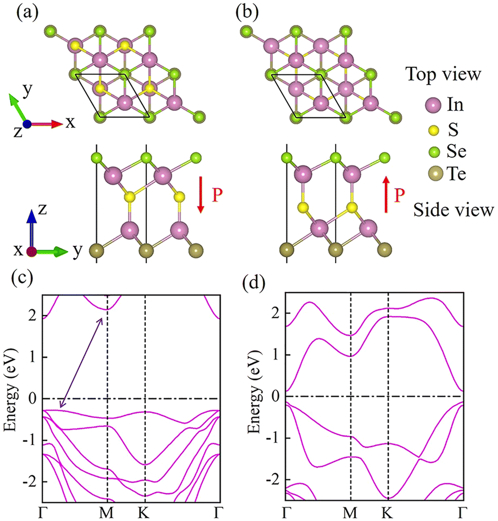
The In2SSeTe monolayers were obtained by replacing S atoms on the surface terminations with Se and Te atoms in the ferroelectric α-In2S3 monolayer. Fig. 1(a) and (b) show the structures of two different ferroelectric states of the proposed In2SSeTe monolayers, for which S atoms sitting right across the lower and upper In atoms are named as In2SSeTe-P↓ and In2SSeTe-P↑, respectively. The optimized lattice constants for In2SSeTe-P↓ and In2SSeTe-P↑ are 4.183 and 4.179 Å, respectively. To check the stability of the proposed In2SSeTe monolayers, the phonon calculations and AIMD simulations were performed, as shown in Fig. S1 (ESI†). Minor imaginary frequencies at Γ points are observed from the phonon dispersion curves. Such minor imaginary frequency could be eliminated by using larger supercells or applying small strain,64,65 revealing that In2SSeTe-P↓ and In2SSeTe-P↑ are stable from the lattice dynamic point of view. Besides, after annealing the In2SSeTe monolayer for 9 ps at 300 K in AIMD simulations, the total energies of In2SSeTe-P↑ and In2SSeTe-P↓ are limited in a narrow window. Also, no significant distortion can be found in the final structures, demonstrating their thermal stabilities.66 Therefore, both the phonon calculations and AIMD simulations confirm the stabilities of In2SSeTe-P↓ and In2SSeTe-P↑, which might verify their feasibility in the experiment. Furthermore, we unravel the electronic structures of the proposed In2SSeTe monolayers. The band structures of In2SSeTe-P↓ and In2SSeTe-P↑ using the HSE06 method are exhibited in Fig. 1(c) and (d), respectively. Both ferroelectric states of In2SSeTe show semiconducting electronic structure features. Herein, In2SSeTe-P↓ holds an indirect band gap, in which its conduction band minimum (CBM) is located at the Γ point, and its valence band maximum (VBM) is located between Γ and M points. On the other hand, In2SSeTe-P↑ has a direct band gap, where both the CBM and VBM are located at the Γ point. Interestingly, the predicted band gaps for In2SSeTe-P↓ and In2SSeTe-P↑ are 2.20 and 0.25 eV, respectively. The significant difference of band gaps will lead to different electron transmission capacities in the application of FTJ devices. It is worth noting that an appropriate electric field could induce the transition between In2SSeTe-P↓ and In2SSeTe-P↑, similar to In2X3 (X = S, Se, Te).67 Therefore, In2SSeTe is a promising candidate for ferroelectric switching devices.
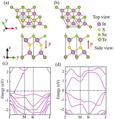 |
| | Fig. 1 The structural schematic diagrams and HSE06 band structures of In2SSeTe monolayers (a) and (c) for In2SSeTe-P↓, (b) and (d) for In2SSeTe-P↑. | |
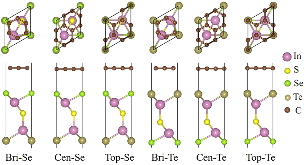
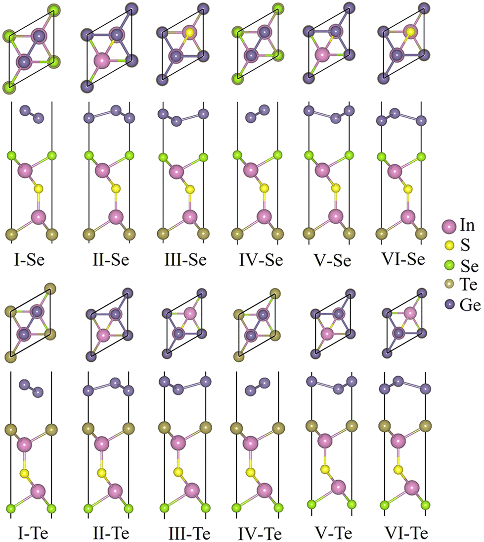
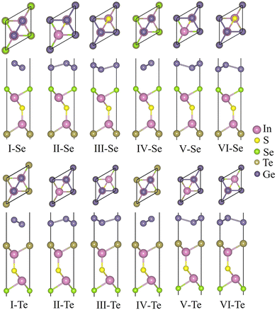
Graphene and germanene possess hexagonal honeycomb structures (see Fig. S2(a) and (b), ESI†) with lattice constants of 2.46 Å and 4.06 Å, respectively. The  graphene and 1 × 1 germanene unit cells show small lattice mismatches of 1.86% and 2.94% with the P↓ state of the In2SSeTe monolayer. The calculated band structures shown in Fig. S2(c) and (d) (ESI†) reveal their linearly dispersing electronic bands at the Fermi level, indicating the intrinsic high carrier mobility of the Dirac fermions in graphene and germanene.68 Herein, we construct the lateral FTJs by employing graphene/In2SSeTe and germanene/In2SSeTe heterostructures as the electrodes. Before building the ferroelectric tunnel junctions (FTJs), In2SSeTe with the P↓ state regarded as the initial state was employed to construct the heterostructures with graphene or germanene to get the most favorable stacking configurations. For graphene/In2SSeTe-P↓ heterostructures, there are three types of stacking configurations, i.e., the atoms of In2SSeTe-P↓ located above either the centers of the hexagons, bonds, or C atoms. As depicted in Fig. 2, six different stacking configurations of graphene/In2SSeTe-P↓ heterostructures are considered due to two different termination surfaces (i.e., Se and Te terminated surfaces) of In2SSeTe-P↓. On the other hand, since each surface of In2SSeTe-P↓ has six different stacking configurations with germanene by shifting and rotating the upper germanene layers, there are twelve different stacking configurations for germanene/In2SSeTe-P↓ heterostructures, as shown in Fig. 3. To determine the most stable stacking configurations, the binding energies (Eb) and formation energies (Ef) of the heterostructures are calculated, which are defined as
| | | Eb = (EtotalH − Efixupper − Efixbottom)/S | (3) |
| | | Ef = (EtotalH − Eupper − Ebottom) | (4) |
where
EtotalH represents the total energy of the heterostructure.
Efixupper and
Efixupper are the total energies of the upper and bottom monolayers constrained in the heterostructure lattice constants, respectively.
S is the heterostructure interfacial area. And
Eupper and
Ebottom stand for the total energies of the freestanding upper and bottom monolayers, respectively.
Tables 1 and 2 list the calculated results for graphene/In
2SSeTe-P
↓ and germanene/In
2SSeTe-P
↓ heterostructures with different stacking configurations, respectively. All the binding energies around −20 meV Å
−2 reveal that the different monolayers are connected by the long range van der Waals (vdW) force. Comparing the calculated
Eb and
Ef for graphene/In
2SSeTe-P
↓ and germanene/In
2SSeTe-P
↓ heterostructures, it is deduced that the interlayer binding force of the germanene/In
2SSeTe-P
↓ heterostructure is stronger than that of the graphene/In
2SSeTe-P
↓ heterostructure. In addition, the Se surface of In
2SSeTe-P
↓ is more energetically favorable to absorb on graphene and germanene than the Te surface. The most stable stacking configurations are Cen-Se type for the graphene/In
2SSeTe-P
↓ heterostructure and I-Se type for the germanene/In
2SSeTe-P
↓ heterostructure. As a result, we will focus on these stable configurations in the following analysis.
 |
| | Fig. 2 The schematic diagrams of different stacking configurations for graphene/In2SSeTe-P↓ heterostructures. | |
 |
| | Fig. 3 The schematic diagrams of different stacking configurations for germanene/In2SSeTe-P↓ heterostructures. | |
Table 1 The binding energies (Eb, meV Å−2) and formation energies (Ef, eV) of different stacking configurations for graphene/In2SSeTe-P↓ heterostructures
| Stacking configuration |
E
b-Se |
E
b-Te |
E
f-Se |
E
f-Te |
| Bridge |
−14.995 |
−14.398 |
−0.180 |
−0.171 |
| Center |
−15.308 |
−14.750 |
−0.186 |
−0.177 |
| Top |
−14.970 |
−14.359 |
−0.181 |
−0.171 |
Table 2 The binding energies (Eb, meV Å−2) and formation energies (Ef, eV) of different stacking configurations for germanene/In2SSeTe-P↓ heterostructures
| Stacking configuration |
E
b-Se |
E
b-Te |
E
f-Se |
E
f-Te |
| I |
−23.482 |
−22.413 |
−0.316 |
−0.300 |
| II |
−18.922 |
−14.920 |
−0.243 |
−0.190 |
| III |
−15.454 |
−15.379 |
−0.200 |
−0.197 |
| IV |
−22.268 |
−22.285 |
−0.299 |
−0.298 |
| V |
−16.062 |
−15.516 |
−0.209 |
−0.199 |
| VI |
−17.507 |
−14.778 |
−0.223 |
−0.188 |
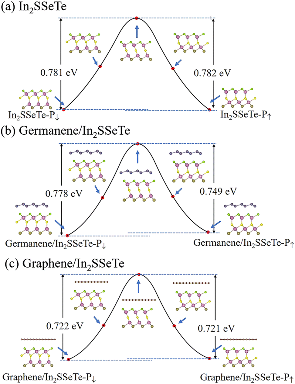
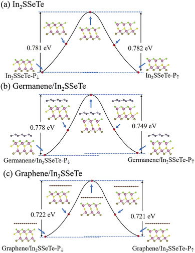
The phase transition energy barriers of the polarization reversal processes are essential for the switching performance of ferroelectric devices.69,70 The most effective polarization reversal pathway without an electric field connects the two degenerate states with different polarities.26 Therefore, we calculated the phase transition process of the activation barrier against direct shifting of the central S layer using the climbing-image nudged elastic band (CINEB) method. As shown in Fig. 4, the energy barriers against direct shifting of the central S layer are 0.781, 0.778 and 0.722 eV per unit cell from In2SSeTe-P↓ to In2SSeTe-P↑, graphene/In2SSeTe-P↓ to graphene/In2SSeTe-P↑ and germanene/In2SSeTe-P↓ to germanene/In2SSeTe-P↑, respectively. On the other hand, the energy barriers of reverse processes are 0.782, 0.749 and 0.721 eV per unit cell from In2SSeTe-P↑ to In2SSeTe-P↓, graphene/In2SSeTe-P↑ to graphene/In2SSeTe-P↓ and germanene/In2SSeTe-P↑ to germanene/In2SSeTe-P↓, respectively. The calculated energy barriers of In2SSeTe are about 0.7–0.8 eV per uc, which are lower than the results of In2Se3 (∼0.85 eV).26 Interestingly, it can be deduced that the heterostructures are easier to realize polarization reversal than the In2SSeTe monolayer.
 |
| | Fig. 4 Kinetics pathways of polarization reversal processes of (a) In2SSeTe, (b) germanene/In2SSeTe heterostructures and (c) graphene/In2SSeTe heterostructures. | |
In2SeTe-P↓ and In2SeTe-P↑ own different electrical conductivities due to their distinguishable electronic structures, which could be one of the physical origins to realize high TER ratios in the corresponding FTJs. At the same time, the different conducting states of the electrodes of graphene/In2SSeTe and germanene/In2SSeTe heterostructures can be another crucial reason for the huge TER ratios of these FTJs. Therefore, we turn our attention to the electronic structures of graphene/In2SSeTe and germanene/In2SSeTe heterostructures, and the results using HSE06 and PBE methods are plotted in Fig. 5 and Fig. S3 (ESI†), respectively. For graphene/In2SSeTe-P↓ and graphene/In2SSeTe-P↑ heterostructures, the projected band structures (PBSs) of graphene, In2SSeTe-P↓ and In2SSeTe-P↑ show the same shape as the band structures of their isolated monolayers using both methods. It is due to graphene and In2SSeTe layers connecting with vdW force, which results in little hybridization between these two layers. The PBSs of heterostructures show an upward or downward shift compared with the band structures of the corresponding monolayers. For the PBSs of graphene/In2SSeTe-P↓ and graphene/In2SSeTe-P↑ heterostructures shown in Fig. 5(a) and (c), the PBS of graphene moves up with respect to the Fermi level, and that of In2SSeTe possesses a conversely downward shift. As shown in Fig. 5(b), for germanene/In2SSeTe-P↓ heterostructures, the PBSs of graphene and In2SSeTe move upward and downward, respectively. However, the PBSs of germanene and In2SSeTe for germanene/In2SSeTe-P↑ heterostructures shown in Fig. 5(d) move downward and upward, respectively, which is converse to that of germanene/In2SSeTe-P↓ heterostructures. The different band structures for the different heterostructures are mainly determined by the interlayer charge transfers, as shown in Fig. S4 (ESI†). It can be seen that In2SSeTe layers obtain electrons and graphene/germanene layers lose electrons for graphene/In2SSeTe-P↓, graphene/In2SSeTe-P↑ and germanene/In2SSeTe-P↓ heterostructures, hence the PBSs of In2SSeTe and graphene or germanene show a downward and upward shift, respectively. Nevertheless, the germanene layer of germanene/In2SSeTe-P↑ heterostructures obtains electrons and the In2SSeTe layer loses electrons, resulting in a converse shift of the projected band structures. Besides, it is noted that the PBSs of In2SSeTe-P↓ for graphene/In2SSeTe-P↓ and the PBSs of In2SSeTe-P↑ for graphene/In2SSeTe-P↑ heterostructures cross the Fermi level, resulting in Ohmic contacts, which can significantly improve the carrier transfer and injection efficiency.71,72 For germanene/In2SSeTe heterostructures, the PBSs of In2SSeTe-P↓ for germanene/In2SSeTe-P↓ heterostructures are separated by the Fermi level showing Schottky contact, which is not beneficial for the carrier transfer. Moreover, the PBSs of germanene/In2SSeTe-P↑ heterostructures show Ohmic contact, which is similar to the graphene/In2SSeTe heterostructures. These results will lead to a more significant difference in conductivity between the P↓ and P↑ states of germanene-based FTJs, indicating that germanene-based FTJs might have a better performance than graphene-based FTJs.
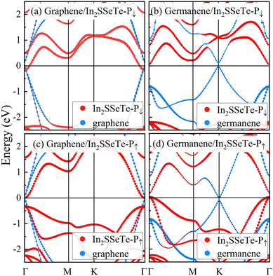 |
| | Fig. 5 The projected band structures of (a) graphene/In2SSeTe-P↓, (b) germanene/In2SSeTe-P↓, (c) graphene/In2SSeTe-P↑ and (d) germanene/In2SSeTe-P↑ heterostructures using the HSE06 method. | |
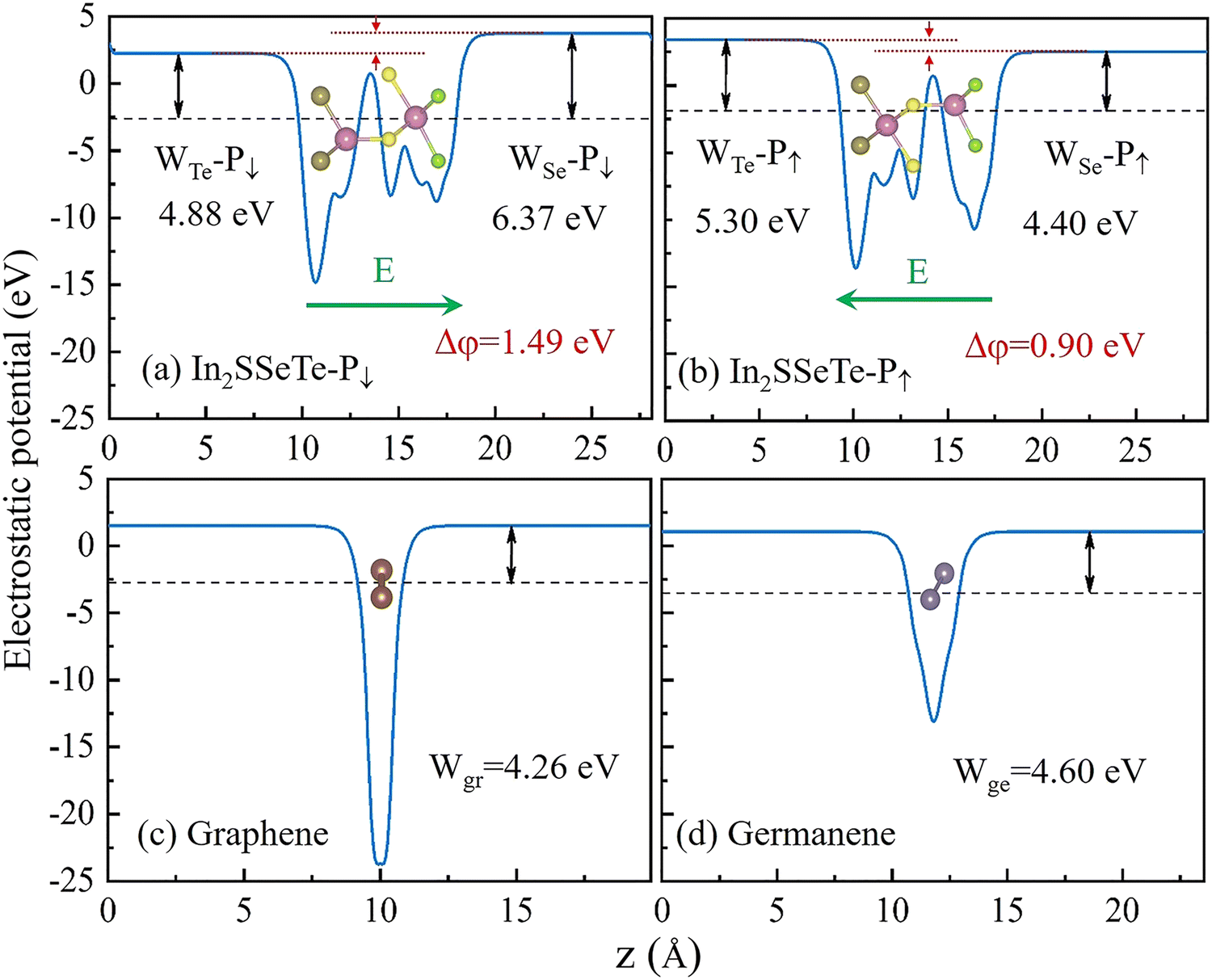
To understand why graphene/In2SSeTe and germanene/In2SSeTe heterostructures show different charge transfer natures, we calculated the electrostatic potential of different isolated monolayers, as depicted in Fig. 6. The work function determines the direction of electron transfer when isolated monolayers form heterostructures,73 as shown in the corresponding figures. For In2SSeTe-P↓ and In2SSeTe-P↑, the work functions of the Te surface of WTe-P↓/WTe-P↑ are different from those of the Se surface due to the broken spatial inversion symmetry. The different work functions on two surfaces will result in a built-in electric field (Δφ). The Δφ of In2SSeTe with the P↓ state is 1.49 eV, hence the direction of the electric field is from the Te surface to the Se surface. The Δφ of In2SSeTe with the P↑ state is 0.90 eV, hence the direction of the electric field is from the Se surface to the Te surface. Besides, the calculated work functions of graphene and germanene are 4.26 eV and 4.60 eV, respectively. When two different two-dimensional materials form a heterostructure, the electrons will flow from the lower work function side to the higher work function side until their Fermi levels are equal.74 Therefore, the work functions of the Se surface of In2SSeTe with P↓ and P↑ states are lower than those of graphene and germanene, and the Se surfaces of In2SSeTe in graphene/In2SSeTe-P↓, graphene/In2SSeTe-P↑ and germanene/In2SSeTe-P↓ heterostructures lose electrons, while graphene/germanene layers gain electrons. Besides, the Se surface of In2SSeTe in germanene/In2SSeTe-P↑ heterostructures gains electrons while graphene/germanene layers lose electrons, due to the work function of the Se surface of In2SSeTe with P↑ states being lower than that of germanene.
 |
| | Fig. 6 The electrostatic potential of (a) and (b) monolayered In2SSeTe with P↓ and P↑, (c) graphene (Wgr) and (d) germanene (Wge). | |
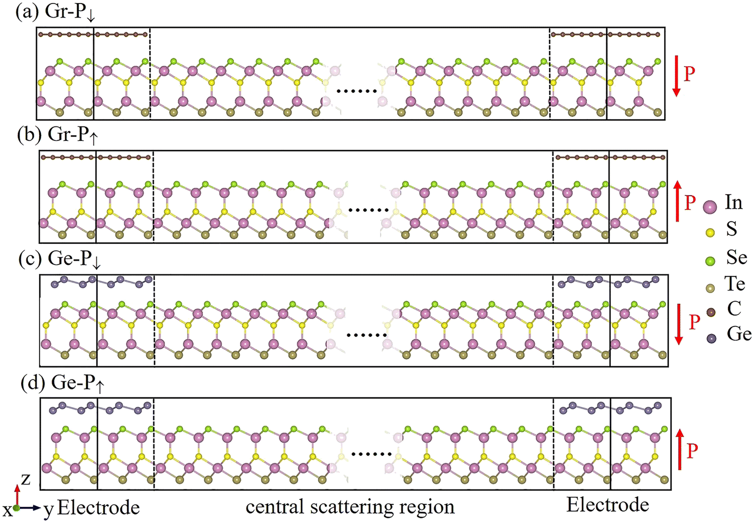
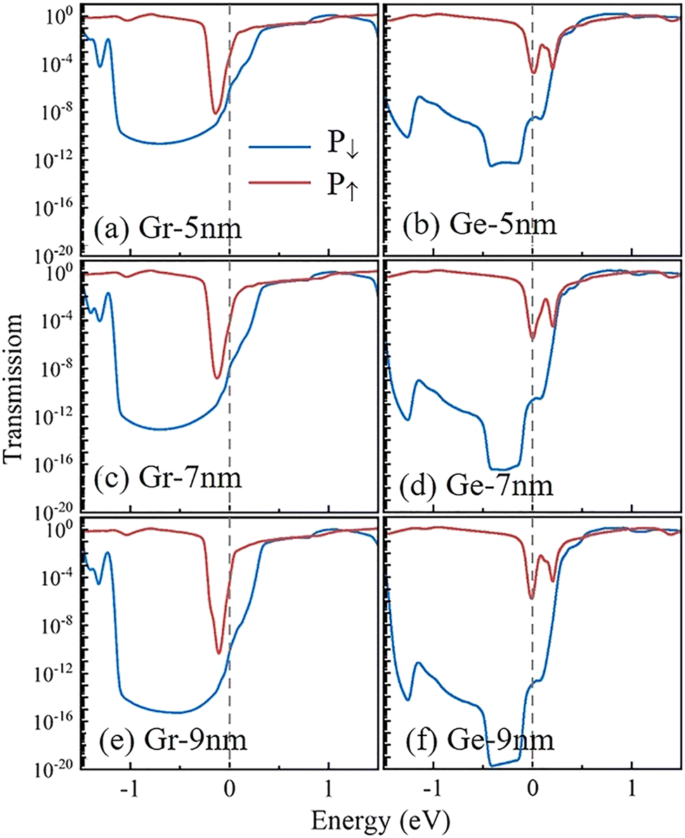
By employing graphene/In2SSeTe and germanene/In2SSeTe heterostructures as the electrodes and In2SSeTe monolayer as the central scattering region, the FTJ models with different polarizations of In2SSeTe (P↓ and P↑) namely Gr-P↓, Gr-P↑, Ge-P↓ and Ge-P↑ FTJs are constructed as shown in Fig. 7. To comprehensively investigate the transport properties versus the lengths of the central scattering region in FTJs, we calculated the electronic transport-related behavior of such FTJs with the central scattering region lengths of 5 nm, 7 nm and 9 nm. The zero-bias transmission coefficient curves are shown in Fig. 8. For the transmission coefficient curves of Gr-P↓ FTJs, there is a sharp dip at −1 eV below the Fermi level and a sharp rise near the Fermi level. As a result, the energy region from −1 eV to −0.2 eV has much lower transmission coefficients. For the transmission coefficient curves of Gr-P↑ FTJs, there is a sharp dip at −0.1 eV below the Fermi level, and the transmission coefficient curves dip to a much deeper level with the central scattering region length increasing from 5 nm to 9 nm. On the other hand, there are two small trenches for the transmission coefficient curves of the Ge-P↑ FTJs with different central scattering region lengths located at the Fermi level and around 0.2 eV, respectively. The lowest transmission region of Ge-P↓ FTJs occurred at −0.4 to −0.1 eV, which shows a distinct magnitude difference from the Ge-P↑ FTJs and implies that huge TER ratios will be achieved below the Fermi level. There is a sharp rise around the Fermi level, and the transmission coefficients are almost coincident when the energy is higher than 0.2 eV, indicating a sharp drop of TER ratios.
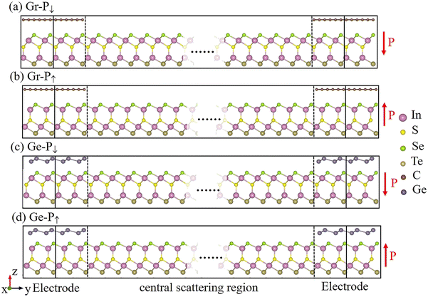 |
| | Fig. 7 The schematic diagrams of the FTJs with downward (P↓) and upward (P↑) polarization. (a) Gr-P↓ and (b) Gr-P↑ FTJs, for the graphene/In2SSeTe heterostructure as electrodes. (c) Ge-P↓ and (d) Ge-P↑ FTJs for the germanene/In2SSeTe heterostructure as electrodes. The lengths of the central scattering regions are set to 5 nm, 7 nm and 9 nm, respectively. | |
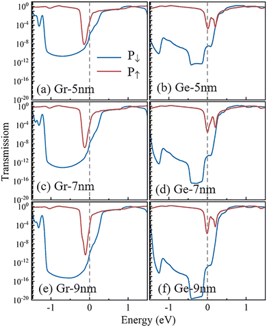 |
| | Fig. 8 The zero-bias transmission coefficient curves for (a), (c) and (e) graphene(Gr)-based FTJs, (b), (d) and (f) germanene (Ge)-based FTJs with the central scattering region lengths of 5 nm, 7 nm and 9 nm. | |
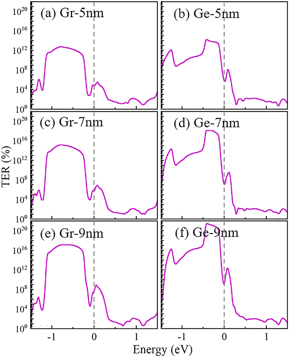
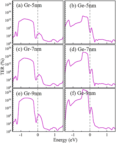
The zero-bias tunnel electroresistance (TER) ratio curves with the energy region from −1.5 eV to 1.5 eV are shown in Fig. 9. The results of graphene-based and germanene-based FTJs are given in the left and right panels, respectively. It should be noted that the highest TER ratios occurred at around −0.7 eV and −0.4 eV for graphene-based and germanene-based FTJs, respectively. The values of the highest TER ratios increase exponentially with the length of the central scattering region. Table 3 summarizes the calculated transmission coefficients and TER ratios at the Fermi level of the Gr-P↓ (TGr-P↓), Gr-P↑ (TGr-P↑), Ge-P↓ (TGe-P↓) and Ge-P↑ (TGe-P↑) FTJs. Herein, the transmission coefficients for the FTJs with P↑ states are much higher than those of the P↓ states, resulting in an apparent TER effect. The best performances are found at the FTJs with 9 nm central scattering region length for both graphene-based and germanene-based FTJs due to their huge TER ratios of 2.24 × 10⁷% and 2.98 × 10⁸%, respectively. Besides, the calculated TER ratios reveal that germanene-based FTJs have better application potential than graphene-based FTJs, regardless of the thickness of the devices, which agrees well with our previous electronic structure analysis.
 |
| | Fig. 9 The zero-bias tunnel electroresistance (TER) ratio curves for (a), (c) and (e) graphene(Gr)-based FTJs; (b), (d) and (f) germanene (Ge)-based FTJs with the central scattering region lengths of 5 nm, 7 nm and 9 nm. | |
Table 3 The transmission coefficients and TER ratios at the Fermi level for the Gr-P↓ (TGr-P↓), Gr-P↑ (TGr-P↑), Ge-P↓ (TGe-P↓) and Ge-P↑ (TGe-P↑) FTJs
| Central scattering region length |
T
Gr-P↓
|
T
Gr-P↑
|
TER ratio |
T
Ge-P↓
|
T
Ge-P↑
|
TER ratio |
| 5 nm |
1.25 × 10⁻⁶ |
4.06 × 10⁻⁴ |
3.24 × 10⁴% |
3.55 × 10⁻⁹ |
8.63 × 10⁻⁶ |
2.43 × 10⁵% |
| 7 nm |
1.88 × 10⁻⁸ |
4.94 × 10⁻⁵ |
2.63 × 10⁵% |
2.54 × 10⁻¹¹ |
6.45 × 10⁻⁷ |
2.54 × 10⁶% |
| 9 nm |
1.33 × 10⁻¹⁰ |
2.99 × 10⁻⁵ |
2.24 × 10⁷% |
1.49 × 10⁻¹³ |
4.42 × 10⁻⁷ |
2.98 × 10⁸% |
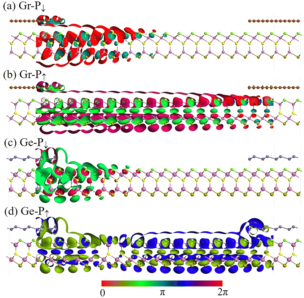
In order to better understand the behaviors of transmission states and transmission channels, the eigenfunctions of 5 nm, 7 nm and 9 nm FTJs for the Fermi level and (kx, ky) = (0, 0) wave vector space were calculated and are plotted in Fig. 10, Fig. S5 and S6 (ESI†), respectively. The transmission channels of the electrons in P↑ and P↓ states are shown as 3D contour plots, the isosurface value is chosen to be 0.02 e.u., which is sufficient to show the contribution of each atom. As shown in Fig. 10(a) and (c), the transmission eigenstates of Gr-P↓ and Ge-P↓ FTJs decay from the left electrode to the right electrode, resulting in electronic states that are only localized at the left part of FTJs. In this case, the electrons cannot pass from the left to the right electrode, and the FTJs are in a high resistance state. As depicted in Fig. 10(b) and (d), the transmission eigenstates of Gr-P↑ and Ge-P↑ FTJs can be found in the whole FTJs, revealing that the electrons can flow effortlessly from the left electrode and right electrode, and this is a typical conductive mode.
 |
| | Fig. 10 The contour plot of the transmission eigenstates at the Fermi level and (kx, ky) = (0, 0) of (a) Gr-P↓, (b) Gr-P↑, (c) Ge-P↓ and (d) Ge-P↑ FTJs with the central scattering region length of 5 nm. The isosurface value is 0.02 a.u. | |
Conclusion
In summary, based on density functional theory and the nonequilibrium Green's function method, we systematically studied two types of lateral ferroelectric tunnel junctions (FTJs) by employing Janus monolayer In2SSeTe as the central scattering region and In2SSeTe/graphene or In2SSeTe/germanene as electrodes. The constructed FTJs have different electrical conductivities when In2SSeTe of the FTJs has P↓ and P↑ states, resulting in an apparent tunneling resistance effect. Except for In2SSeTe with P↓ and P↑ states of the central scattering regions showing different electrical conductivities due to the difference in monolayer band structures, the different conducting behaviors of In2SSeTe in the electrode regions can be another crucial reason for the huge TER ratios. Further analysis indicates that the different conducting behaviors of In2SSeTe in the electrodes arise from the difference in work functions of the two surfaces of In2SSeTe. To determine the length dependence on the performance of FTJs, we investigated the electronic transport-related behavior of graphene and germanene-based FTJs with 5 nm, 7 nm and 9 nm central scattering region lengths. The results show that the TER ratios of both types of FTJs increased with the increase of the device length, and the maximum TER ratios were 2.24 × 10⁷% and 2.98 × 10⁸% for graphene and germanene-based FTJs with 9 nm central scattering region length. These results reveal that such FTJs show great potential application in nonvolatile memory devices.
Author contributions
Zhou Cui: Investigation, formal analysis, and writing – original draft. Ting Li: data curation, and validation. Rui Xiong: data curation and validation. Cuilian Wen: visualization, formal analysis, and writing – review & editing. Yinggan Zhang: formal analysis and writing – review & editing. Jingying Zheng: formal analysis and writing – review & editing. Bo Wu: writing – review & editing. Baisheng Sa: project administration, supervision, and writing –review & editing.
Conflicts of interest
The authors declare no competing financial interest.
Acknowledgements
This work was supported by the National Key Research and Development Program of China (No. 2022YFB3807200), the National Natural Science Foundation of China (No. 21973012, 21905050 and 52201022), the Natural Science Foundation of Fujian Province (No. 2021J06011, 2020J01351, 2020J01474, 2021H6011 and 2021J01590), and the ‘‘Qishan Scholar’’ Scientific Research Project of Fuzhou University.
References
- C. R. Bowen, H. A. Kim, P. M. Weaver and S. Dunn, Piezoelectric and ferroelectric materials and structures for energy harvesting applications, Energy Environ. Sci., 2014, 7, 25–44 RSC.
- L. W. Martin and A. M. Rappe, Thin-film ferroelectric materials and their applications, Nat. Rev. Mater., 2016, 2, 1–14 Search PubMed.
- M. Wu, S. Dong, K. Yao, J. Liu and X. C. Zeng, Ferroelectricity in Covalently functionalized Two-dimensional Materials: Integration of High-mobility Semiconductors and Nonvolatile Memory, Nano Lett., 2016, 16, 7309–7315 CrossRef CAS PubMed.
- Q. Yang, T. Zhong, Z. Tu, L. Zhu, M. Wu and X. C. Zeng, Design of Single-Molecule Multiferroics for Efficient Ultrahigh-Density Nonvolatile Memories, Adv. Sci., 2019, 6, 1801572 CrossRef PubMed.
- A. Gruverman, D. Wu, H. Lu, Y. Wang, H. W. Jang, C. M. Folkman, M. Y. Zhuravlev, D. Felker, M. Rzchowski, C. B. Eom and E. Y. Tsymbal, Tunneling electroresistance effect in ferroelectric tunnel junctions at the nanoscale, Nano Lett., 2009, 9, 3539–3543 CrossRef CAS PubMed.
- R. Soni, A. Petraru, P. Meuffels, O. Vavra, M. Ziegler, S. K. Kim, D. S. Jeong, N. A. Pertsev and H. Kohlstedt, Giant electrode effect on tunnelling electroresistance in ferroelectric tunnel junctions, Nat. Commun., 2014, 5, 5414 CrossRef PubMed.
- X. K. Duan, H. Wang, X. F. Chen and J. S. Qi, Multiple polarization phases and strong magnetoelectric coupling in the layered transition metal phosphorus chalcogenides TMP2X6(T = Cu, Ag; M = Cr, V; X = S, Se) by controlling the interlayer interaction and dimension, Phys. Rev. B, 2022, 106, 115403 CrossRef CAS.
- F. Fan, B. Luo, M. Duan, H. Xing, K. Jin and C. Chen, Ferroelectric domain switching investigation of BiFeO3 thin film on Pt/Ti/SiO2/Si (111) substrate, Appl. Surf. Sci., 2012, 258, 7412–7416 CrossRef CAS.
- Q. Pan, Z. B. Liu, Y. Y. Tang, P. F. Li, R. W. Ma, R. Y. Wei, Y. Zhang, Y. M. You, H. Y. Ye and R. G. Xiong, A Three-Dimensional Molecular Perovskite Ferroelectric: (3-Ammoniopyrrolidinium)RbBr3, J. Am. Chem. Soc., 2017, 139, 3954–3957 CrossRef CAS PubMed.
- L. L. Tao and J. Wang, Ferroelectricity and tunneling electroresistance effect driven by asymmetric polar interfaces in all-oxide ferroelectric tunnel junctions, Appl. Phys. Lett., 2016, 108, 062903 CrossRef.
- V. S. Borisov, S. Ostanin, S. Achilles, J. Henk and I. Mertig, Spin-dependent transport in a multiferroic tunnel junction: Theory for Co/PbTiO3/Co, Phys. Rev. B: Condens. Matter Mater. Phys., 2015, 92, 075137 CrossRef.
- C. Li, L. Huang, T. Li, W. Lu, X. Qiu, Z. Huang, Z. Liu, S. Zeng, R. Guo, Y. Zhao, K. Zeng, M. Coey, J. Chen, Ariando and T. Venkatesan, Ultrathin BaTiO3-based ferroelectric tunnel junctions through interface engineering, Nano Lett., 2015, 15, 2568–2573 CrossRef CAS PubMed.
- W. Xiao, L. Kang, H. Hao, Y. Zhou, X. Zheng, L. Zhang and Z. Zeng, Giant Tunneling Electroresistance Induced by Interfacial Doping in Pt/BaTiO3/Pt Ferroelectric Tunnel Junctions, Phys. Rev. A: At., Mol., Opt. Phys., 2022, 17, 044001 CAS.
- Z. Xi, J. Ruan, C. Li, C. Zheng, Z. Wen, J. Dai, A. Li and D. Wu, Giant tunnelling electroresistance in metal/ferroelectric/semiconductor tunnel junctions by engineering the Schottky barrier, Nat. Commun., 2017, 8, 15217 CrossRef CAS PubMed.
- D. D. Fong, G. B. Stephenson, S. K. Streiffer, J. A. Eastman, O. Auciello, P. H. Fuoss and C. Thompson, Ferroelectricity in ultrathin perovskite films, Science, 2004, 304, 1650 CrossRef CAS PubMed.
- M. Trieloff, E. K. Jessberger, I. Herrwerth, J. Hopp, C. Fieni, M. Ghelis, M. Bourot-Denise and P. Pellas, Structure and thermal history of the H-chondrite parent asteroid revealed by thermochronometry, Nature, 2003, 422, 506 CrossRef.
- Y. S. Kim, D. H. Kim, J. D. Kim, Y. J. Chang, T. W. Noh, J. H. Kong, K. Char, Y. D. Park, S. D. Bu, J. G. Yoon and J. S. Chung, Critical thickness of ultrathin ferroelectric BaTiO3 films, Appl. Phys. Lett., 2005, 86, 102907 CrossRef.
- M. Stengel and N. A. Spaldin, Origin of the dielectric dead layer in nanoscale capacitors, Nature, 2006, 443, 679–682 CrossRef CAS PubMed.
- K. S. Novoselov, A. K. Geim, S. V. Morozov, D. Jiang, Y. Zhang, S. V. Dubonos, I. V. Grigorieva and A. A. Firsov, Electric Field Effect in Atomically Thin Carbon Films, Science, 2004, 306, 666–669 CrossRef CAS PubMed.
- D. S. Schulman, A. J. Arnold and S. Das, Contact engineering for 2D materials and devices, Chem. Soc. Rev., 2018, 47, 3037–3058 RSC.
- R. F. Li, X. J. Yu, C. L. Wen, Y. G. Zhang, H. L. Lin and B. S. Sa, Unexpected Carrier Mobility Anisotropy in the Two-dimensional Ca2Si Monolayer from First-principles Calculations, Chin. J. Struct. Chem., 2020, 39, 1243–1251 Search PubMed.
- X. Wang, J. Xu, J. Si, B. Wang and W. Yin, Semiconductor-metal transition caused by increased surface charge in two-dimensional quintuple-layers Al2O3 materials, Appl. Surf. Sci., 2023, 610, 155614 CrossRef CAS.
- A. Belianinov, Q. He, A. Dziaugys, P. Maksymovych, E. Eliseev, A. Borisevich, A. Morozovska, J. Banys, Y. Vysochanskii and S. V. Kalinin, CuInP2S6 Room Temperature Layered Ferroelectric, Nano Lett., 2015, 15, 3808–3814 CrossRef CAS PubMed.
- F. Liu, L. You, K. L. Seyler, X. Li, P. Yu, J. Lin, X. Wang, J. Zhou, H. Wang, H. He, S. T. Pantelides, W. Zhou, P. Sharma, X. Xu, P. M. Ajayan, J. Wang and Z. Liu, Room-temperature ferroelectricity in CuInP2S6 ultrathin flakes, Nat. Commun., 2016, 7, 12357 CrossRef CAS PubMed.
- M. Chyasnavichyus, M. A. Susner, A. V. Ievlev, E. A. Eliseev, S. V. Kalinin, N. Balke, A. N. Morozovska, M. A. McGuire and P. Maksymovych, Size-effect in layered ferrielectric CuInP2S6, Appl. Phys. Lett., 2016, 109, 172901 CrossRef.
- W. Ding, J. Zhu, Z. Wang, Y. Gao, D. Xiao, Y. Gu, Z. Zhang and W. Zhu, Prediction of intrinsic two-dimensional ferroelectrics in In2Se3 and other III2-VI3 van der Waals materials, Nat. Commun., 2017, 8, 14956 CrossRef CAS PubMed.
- Y. Zhou, D. Wu, Y. Zhu, Y. Cho, Q. He, X. Yang, K. Herrera, Z. Chu, Y. Han, M. C. Downer, H. Peng and K. Lai, Out-of-Plane Piezoelectricity and Ferroelectricity in Layered alpha-In2Se3 Nanoflakes, Nano Lett., 2017, 17, 5508–5513 CrossRef CAS PubMed.
- R. Fei, W. Kang and L. Yang, Ferroelectricity and Phase Transitions in Monolayer Group-IV Monochalcogenides, Phys. Rev. Lett., 2016, 117, 097601 CrossRef PubMed.
- H. Wang and X. Qian, Giant Optical Second Harmonic Generation in Two-Dimensional Multiferroics, Nano Lett., 2017, 17, 5027–5034 CrossRef CAS PubMed.
- L. Qi, S. Ruan and Y. J. Zeng, Review on Recent Developments in 2D Ferroelectrics: Theories and Applications, Adv. Mater., 2021, 33, e2005098 CrossRef PubMed.
- X. W. Shen, Y. W. Fang, B. B. Tian and C. G. Duan, Two-Dimensional Ferroelectric Tunnel Junction: The Case of Monolayer In:SnSe/SnSe/Sb:SnSe Homostructure, ACS Appl. Electron. Mater., 2019, 1, 1133–1140 CrossRef CAS.
- L. Kang, P. Jiang, H. Hao, Y. Zhou, X. Zheng, L. Zhang and Z. Zeng, Giant tunnel electroresistance in ferroelectric tunnel junctions with metal contacts to two-dimensional ferroelectric materials, Phys. Rev. B, 2021, 103, 125414 CrossRef CAS.
- L. Kang, P. Jiang, H. Hao, Y. Zhou, X. Zheng, L. Zhang and Z. Zeng, Giant tunneling electroresistance in two-dimensional ferroelectric tunnel junctions with out-of-plane ferroelectric polarization, Phys. Rev. B, 2020, 101, 014105 CrossRef CAS.
- R. Li, Y. Cheng and W. Huang, Recent Progress of Janus 2D Transition Metal Chalcogenides: From Theory to Experiments, Small, 2018, 14, e1802091 CrossRef PubMed.
- Z. Zhou, X. Niu, Y. Zhang and J. Wang, Janus MoSSe/WSeTe heterostructures: a direct Z-scheme photocatalyst for hydrogen evolution, J. Mater. Chem. A, 2019, 7, 21835–21842 RSC.
- L. Dong, J. Lou and V. B. Shenoy, Large In-Plane and Vertical Piezoelectricity in Janus Transition Metal Dichalchogenides, ACS Nano, 2017, 11, 8242–8248 CrossRef CAS PubMed.
- P. Wang, H. Liu, Y. Zong, H. Wen, J. B. Xia and H. B. Wu, Two-Dimensional In2X2X' (X and X' = S, Se, and Te) Monolayers with an Intrinsic Electric Field for High-Performance Photocatalytic and Piezoelectric Applications, ACS Appl. Mater. Interfaces, 2021, 13, 34178–34187 CrossRef CAS PubMed.
- C. Cui, F. Xue, W. Hu and L. Li, Two-dimensional materials with piezoelectric and ferroelectric functionalities, npj 2D Mater. Appl., 2018, 2, 1–14 CrossRef.
- B. Hunt, J. D. Sanchez-Yamagishi, A. F. Young, M. Yankowitz, B. J. LeRoy, K. Watanabe, T. Taniguchi, P. Moon, M. Koshino, P. Jarillo-Herrero and R. C. Ashoori, Massive Dirac fermions and Hofstadter butterfly in a van der Waals heterostructure, Science, 2013, 340, 1427–1430 CrossRef CAS PubMed.
- L. A. Ponomarenko, R. V. Gorbachev, G. L. Yu, D. C. Elias, R. Jalil, A. A. Patel, A. Mishchenko, A. S. Mayorov, C. R. Woods, J. R. Wallbank, M. Mucha-Kruczynski, B. A. Piot, M. Potemski, I. V. Grigorieva, K. S. Novoselov, F. Guinea, V. I. Fal'ko and A. K. Geim, Cloning of Dirac fermions in graphene superlattices, Nature, 2013, 497, 594–597 CrossRef CAS PubMed.
- Z. Wang, Q. Chen and J. Wang, Electronic Structure of Twisted Bilayers of Graphene/MoS2 and MoS2/MoS2, J. Phys. Chem. C, 2015, 119, 4752–4758 CrossRef CAS.
- X. Yang, B. Sa, P. Lin, C. Xu, Q. Zhu, H. Zhan and Z. Sun, Tunable Contacts in Graphene/InSe van der Waals Heterostructures, J. Phys. Chem. C, 2020, 124, 23699–23706 CrossRef CAS.
- Z. Zhu, X. Chen, W. Li and J. Qi, Electric field control of the semiconductor-metal transition in two dimensional CuInP2S6/germanene van der Waals heterostructure, Appl. Phys. Lett., 2019, 114, 223102 CrossRef.
- R. Xiong, W. Li, Y. Zhang, Z. Cui, C. Wen, M. Anpo, B. Wu and B. Sa, Computational discovery of In2XY2 (X, Y = S, Se, and Te; X ≠ Y) monolayers as multifunctional energy conversion materials, J. Mater. Chem. C, 2022, 10, 10480–10490 RSC.
- G. Wang, K. Li, L. Peng, Y. Zhang, J. Zhou and Z. Sun, High-Throughput Automatic Integrated Material Calculations and Data Management Intelligent Platform and the Application in Novel Alloys, Acta Metall. Sinica, 2022, 58, 75–88 Search PubMed.
- G. Wang, L. Peng, K. Li, L. Zhu, J. Zhou, N. Miao and Z. Sun, ALKEMIE: An intelligent computational platform for accelerating materials discovery and design, Comput. Mater. Sci., 2021, 186, 110064 CrossRef CAS.
- G. Kresse and J. Furthmüller, Efficient iterative schemes for ab initio total-energy calculations using a plane-wave basis set, Phys. Rev. B: Condens. Matter Mater. Phys., 1996, 54, 11169 CrossRef CAS PubMed.
- J. P. Perdew, K. Burke and M. Ernzerhof, Generalized Gradient Approximation Made Simple, Phys. Rev. Lett., 1996, 77, 3865 CrossRef CAS PubMed.
- S. Grimme, J. Antony, S. Ehrlich and H. Krieg, A consistent and accurate ab initio parametrization of density functional dispersion correction (DFT-D) for the 94 elements H-Pu, J. Chem. Phys., 2010, 132, 154104 CrossRef PubMed.
- S. Grimme, S. Ehrlich and L. Goerigk, Effect of the damping function in dispersion corrected density functional theory, J. Comput. Chem., 2011, 32, 1456–1465 CrossRef CAS PubMed.
- X. Gonze and C. Lee, Dynamical matrices, Born effective charges, dielectric permittivity tensors, and interatomic force constants from density-functional perturbation theory, Phys. Rev. B: Condens. Matter Mater. Phys., 1997, 55, 10355 CrossRef CAS.
- S. Nosé, A unified formulation of the constant temperature molecular dynamics methods, J. Chem. Phys., 1984, 81, 511–519 CrossRef.
- W. G. Hoover, Canonical dynamics: Equilibrium phase-space distributions, Phys. Rev. A: At., Mol., Opt. Phys., 1985, 31, 1695–1697 CrossRef PubMed.
- L. Bengtsson, Dipole correction for surface supercell calculations, Phys. Rev. B: Condens. Matter Mater. Phys., 1999, 59, 12301–12304 CrossRef CAS.
- J. Heyd, G. E. Scuseria and M. Ernzerhof, Hybrid functionals based on a screened Coulomb potential, J. Chem. Phys., 2003, 118, 8207–8215 CrossRef CAS.
- D. Sheppard, R. Terrell and G. Henkelman, Optimization methods for finding minimum energy paths, J. Chem. Phys., 2008, 128, 134106 CrossRef PubMed.
- G. Henkelman and H. Jónsson, Improved tangent estimate in the nudged elastic band method for finding minimum energy paths and saddle points, J. Chem. Phys., 2000, 113, 9978–9985 CrossRef CAS.
- M. Brandbyge, J. L. Mozos, P. Ordejón, J. Taylor and K. Stokbro, Density-functional method for nonequilibrium electron transport, Phys. Rev. B: Condens. Matter Mater. Phys., 2002, 65, 165401 CrossRef.
- S. Smidstrup, T. Markussen, P. Vancraeyveld, J. Wellendorff, J. Schneider, T. Gunst, B. Verstichel, D. Stradi, P. A. Khomyakov, U. G. Vej-Hansen, M. E. Lee, S. T. Chill, F. Rasmussen, G. Penazzi, F. Corsetti, A. Ojanpera, K. Jensen, M. L. N. Palsgaard, U. Martinez, A. Blom, M. Brandbyge and K. Stokbro, QuantumATK: an integrated platform of electronic and atomic-scale modelling tools, J. Phys.: Condens. Matter, 2020, 32, 015901 CrossRef CAS PubMed.
- M. J. van Setten, M. Giantomassi, E. Bousquet, M. J. Verstraete, D. R. Hamann, X. Gonze and G. M. Rignanese, The PseudoDojo: Training and grading a 85 element optimized norm-conserving pseudopotential table, Comput. Phys. Commun., 2018, 226, 39–54 CrossRef CAS.
- V. Blum, R. Gehrke, F. Hanke, P. Havu, V. Havu, X. Ren, K. Reuter and M. Scheffler, Ab initio molecular simulations with numeric atom-centered orbitals, Comput. Phys. Commun., 2009, 180, 2175–2196 CrossRef CAS.
- R. Landauer, Electrical resistance of disordered one-dimensional lattices, Philos. Mag., 2006, 21, 863–867 CrossRef.
- J. P. Velev, C. G. Duan, J. Burton, A. Smogunov, M. K. Niranjan, E. Tosatti, S. Jaswal and E. Y. Tsymbal, Magnetic tunnel junctions with ferroelectric barriers: prediction of four resistance states from first principles, Nano Lett., 2009, 9, 427–432 CrossRef CAS PubMed.
- A. J. Mannix, X. F. Zhou, B. Kiraly, J. D. Wood, D. Alducin, B. D. Myers, X. Liu, B. L. Fisher, U. Santiago, J. R. Guest, M. J. Yacaman, A. Ponce, A. R. Oganov, M. C. Hersam and N. P. Guisinger, Synthesis of borophenes: Anisotropic, two-dimensional boron polymorphs, Science, 2015, 350, 1513–1516 CrossRef CAS PubMed.
- E. S. Penev, A. Kutana and B. I. Yakobson, Can Two-Dimensional Boron Superconduct?, Nano Lett., 2016, 16, 2522–2526 CrossRef CAS PubMed.
- N. Miao, B. Xu, N. C. Bristowe, J. Zhou and Z. Sun, Tunable Magnetism and Extraordinary Sunlight Absorbance in Indium Triphosphide Monolayer, J. Am. Chem. Soc., 2017, 139, 11125–11131 CrossRef CAS PubMed.
- J. Ding, D. F. Shao, M. Li, L. W. Wen and E. Y. Tsymbal, Two-Dimensional Antiferroelectric Tunnel Junction, Phys. Rev. Lett., 2021, 126, 057601 CrossRef CAS PubMed.
- B. Sa and Z. Sun, Electron interactions and Dirac fermions in graphene-Ge2Sb2Te5 superlattices, J. Appl. Phys., 2014, 115, 233714 CrossRef.
- Z. Wen and D. Wu, Ferroelectric Tunnel Junctions: Modulations on the Potential Barrier, Adv. Mater., 2020, 32, e1904123 Search PubMed.
- Y. Q. Li, X. Y. Wang, S. Y. Zhu, D. S. Tang, Q. W. He and X. C. Wang, Enhanced vertical polarization and ultra-low polarization switching barriers of two-dimensional SnS/SnSSe ferroelectric heterostructures, J. Mater. Chem. C, 2022, 10, 12132–12140 RSC.
- Y. Shu, K. He, R. Xiong, Z. Cui, X. Yang, C. Xu, J. Zheng, C. Wen, B. Wu and B. Sa, Strain engineering on the electronic properties and interface contact of graphene/GeN3 van der Waals heterostructure, Appl. Surf. Sci., 2022, 604, 154540 CrossRef CAS.
- D. G. Popescu, M. A. Husanu, C. Chirila, L. Pintilie and C. M. Teodorescu, The interplay of work function and polarization state at the Schottky barriers height for Cu/BaTiO3 interface, Appl. Surf. Sci., 2020, 502, 144101 CrossRef CAS.
- J. Kang, W. Liu, D. Sarkar, D. Jena and K. Banerjee, Computational Study of Metal Contacts to Monolayer Transition-Metal Dichalcogenide Semiconductors, Phys. Rev. X, 2014, 4, 031005 CAS.
- M. K. Mohanta and A. De, Sarkar, Giant tunability in electrical contacts and doping via inconsiderable normal electric field strength or gating for a high-performance in ultrathin field effect transistors based on 2D BX/graphene (X = P, As) van der Waals heterobilayer, Appl. Surf. Sci., 2020, 526, 146749 CrossRef CAS.
|
| This journal is © The Royal Society of Chemistry 2023 |
Click here to see how this site uses Cookies. View our privacy policy here. 
 Open Access Article
 This Open Access Article is licensed under a
  *a,
Yinggan
Zhang
b,
Jingying
Zheng
a,
Bo
Wu
a and
Baisheng
Sa
*a,
Yinggan
Zhang
b,
Jingying
Zheng
a,
Bo
Wu
a and
Baisheng
Sa
 is the k-point averaged transmission function at energy E, and T(k‖,E) is the k-resolved transmission function with k‖ = kx. The tunnel electroresistance (TER) ratio is calculated by the formula63
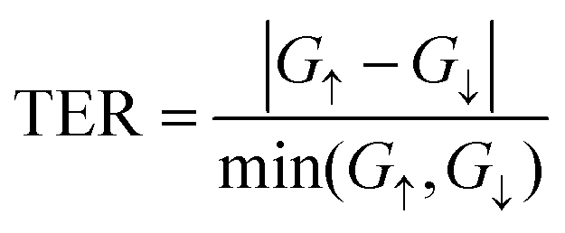
 graphene and 1 × 1 germanene unit cells show small lattice mismatches of 1.86% and 2.94% with the P↓ state of the In2SSeTe monolayer. The calculated band structures shown in Fig. S2(c) and (d) (ESI†) reveal their linearly dispersing electronic bands at the Fermi level, indicating the intrinsic high carrier mobility of the Dirac fermions in graphene and germanene.68 Herein, we construct the lateral FTJs by employing graphene/In2SSeTe and germanene/In2SSeTe heterostructures as the electrodes. Before building the ferroelectric tunnel junctions (FTJs), In2SSeTe with the P↓ state regarded as the initial state was employed to construct the heterostructures with graphene or germanene to get the most favorable stacking configurations. For graphene/In2SSeTe-P↓ heterostructures, there are three types of stacking configurations, i.e., the atoms of In2SSeTe-P↓ located above either the centers of the hexagons, bonds, or C atoms. As depicted in Fig. 2, six different stacking configurations of graphene/In2SSeTe-P↓ heterostructures are considered due to two different termination surfaces (i.e., Se and Te terminated surfaces) of In2SSeTe-P↓. On the other hand, since each surface of In2SSeTe-P↓ has six different stacking configurations with germanene by shifting and rotating the upper germanene layers, there are twelve different stacking configurations for germanene/In2SSeTe-P↓ heterostructures, as shown in Fig. 3. To determine the most stable stacking configurations, the binding energies (Eb) and formation energies (Ef) of the heterostructures are calculated, which are defined as