
 Open Access Article
 This Open Access Article is licensed under a
 Creative Commons Attribution 3.0 Unported Licence
AZABODIPY aggregates as a promising electroluminescent material for sustainable NIR OLED applications†
Wojciech
Mróz‡
 *ab,
Benedetta Maria
Squeo‡
a,
Barbara
Vercelli
c,
Chiara
Botta
a and
Mariacecilia
Pasini
a
*ab,
Benedetta Maria
Squeo‡
a,
Barbara
Vercelli
c,
Chiara
Botta
a and
Mariacecilia
Pasini
a
aIstituto di Scienze e Tecnologie Chimiche (SCITEC), Consiglio Nazionale delle Ricerche, via A. Corti 12, 20133 Milan, Italy. E-mail: wojciech.mroz@scitec.cnr.it
bCenter for Nano Science and Technology (CNST@PoliMi), Istituto Italiano di Tecnologia, via G. Pascoli 70/3, 20133 Milan, Italy
cIstituto di Chimica della Materia Condensata e di Tecnologie per l’Energia (ICMATE), Consiglio Nazionale delle Ricerche, via Cozzi, 53, 20125 Milano, Italy
First published on 16th March 2023
Abstract
Organic materials capable of emission in the near infrared (NIR) spectral range are of great interest for many branches of science and technology. In this work we investigate a NIR emitting molecule (DTDPAB) based on 4,4-difluoro-4-bora-3a,4a-diaza-s-indacene (BODIPY) modified with nitrogen substitution at the carbon meso position (AZABODIPY) and thiophens and phenyls substituents. The thienyl substituents decrease the energy band gap of the molecule with respect to standard AZABODIPY and the emission spectrum results strongly shifted to the lower energies. The molecule is employed as a dopant in commercial and suitably synthesized polymers used as hosts in solution-processable emitting layers of organic light-emitting diodes (OLEDs). After device architecture optimization the electroluminescence in pure NIR (>700 nm) with the maximum at 910 nm is achieved. To our knowledge, this is the first example of electroluminescence from a single AZABODIPY emitter in real NIR, which adds another type of electrically excitable organic luminophore to the family of NIR emitting materials.
Introduction
The demand for materials capable of emitting in the near-infrared (NIR), the electromagnetic radiation in the wavelength range between 700 and 2500 nm, is constantly growing. This spectral range is useful for many applications such as sensors, optical communication, night vision, biometric identification, etc.1–4NIR organic emitters are particularly interesting because they can combine the characteristics of lightness, transparency, and flexibility with the demands of low toxicity and abundance of raw materials, or even better, raw materials that are renewable or derived from waste. This request is representative of the circular economy scheme, one of the pillars of current sustainable development.
The field of organic emitting materials ranges from small molecules to polymers and involves different photophysical mechanisms such as fluorescence, phosphorescence, energy transfer, TADF (thermally activated delayed fluorescence) and AIE (aggregation-induced emission).5–9
The results obtained by applying these materials for example in OLED devices are manifold. In fact, since the pioneering work of Tang and VanSlyke in 1987, OLEDs are now one of the best display technologies in the industry with many electronic appliances, such as TV screens, or smartwatches or mobile phones or cameras. This is due to noteworthy advantages, such as low cost, low-driving voltage, light weightiness, and fast response.10 Furthermore, this technology was regarded as the future major display and lighting technology with application in sensing, biomedicine or automotive.11
Satisfactory results have been obtained in OLEDs with emitting materials from blue to red and with white emission, while the demand for good emitters in NIR is still open.12–16 In fact, currently the main NIR emitters are based on rare earths which have a limited availability and are unevenly distributed in different countries. Therefore, organic materials have been extensively studied for their emissive properties, especially for biolabeling in solution. Recently OLED devices with emission in the NIR zone have been developed thanks to a proper choice of the number, type and position of substituents.2,17–21
Among the organic materials, BODIPY (4,4-difluoro-4-bora-3a,4a-diaza-s-indacene) derivatives are proving to be particularly promising for their chemical stability and excellent absorption and emission properties. Moreover, thanks to nine reactive positions, in BODIPY derivatives a fine modulation of the absorption and emission zone is allowed.22–26
To shift the emission towards the NIR region in 2002 Killoran et al. proposed the replacement of carbon in the meso position with a nitrogen leading to a new family of BODIPY derivatives, known as AZABODIPY, with a marked red shift of the absorption and emission window.27 The formation of a C![[double bond, length as m-dash]](https://www.rsc.org/images/entities/char_e001.gif) N linkage isoelectronic with CC bond but with different electronegativity favours the stabilization of the LUMO state reducing the energy gap. The AZABODIPY derivatives have already found application in solutions for sensing, biological detection and medical imaging28,29 while examples of their use in OLEDs is not reported. The closest analogue employed as an emitter in electroluminescent diode is a dimeric aza-BODIPY called “pyrrolopyrrole” aza-BODIPY.30 On the other hand, devices with reasonable efficiencies based on deep-red and NIR electroluminescence (EL) from BODIPY derivatives can be found in the literature.31–35
N linkage isoelectronic with CC bond but with different electronegativity favours the stabilization of the LUMO state reducing the energy gap. The AZABODIPY derivatives have already found application in solutions for sensing, biological detection and medical imaging28,29 while examples of their use in OLEDs is not reported. The closest analogue employed as an emitter in electroluminescent diode is a dimeric aza-BODIPY called “pyrrolopyrrole” aza-BODIPY.30 On the other hand, devices with reasonable efficiencies based on deep-red and NIR electroluminescence (EL) from BODIPY derivatives can be found in the literature.31–35
In the present work we propose the use in OLED of the asymmetric AZABODIPY which is substituted in 1 and 7 positions with phenyl rings and in 3 and 5 positions with thiophenic fragments (DTDPAB, see Scheme 1). The electron-rich thienyl moiety increases the delocalization (conjugation) with a consequent further shift of the absorption and emission towards low energies in the NIR zone.36,37
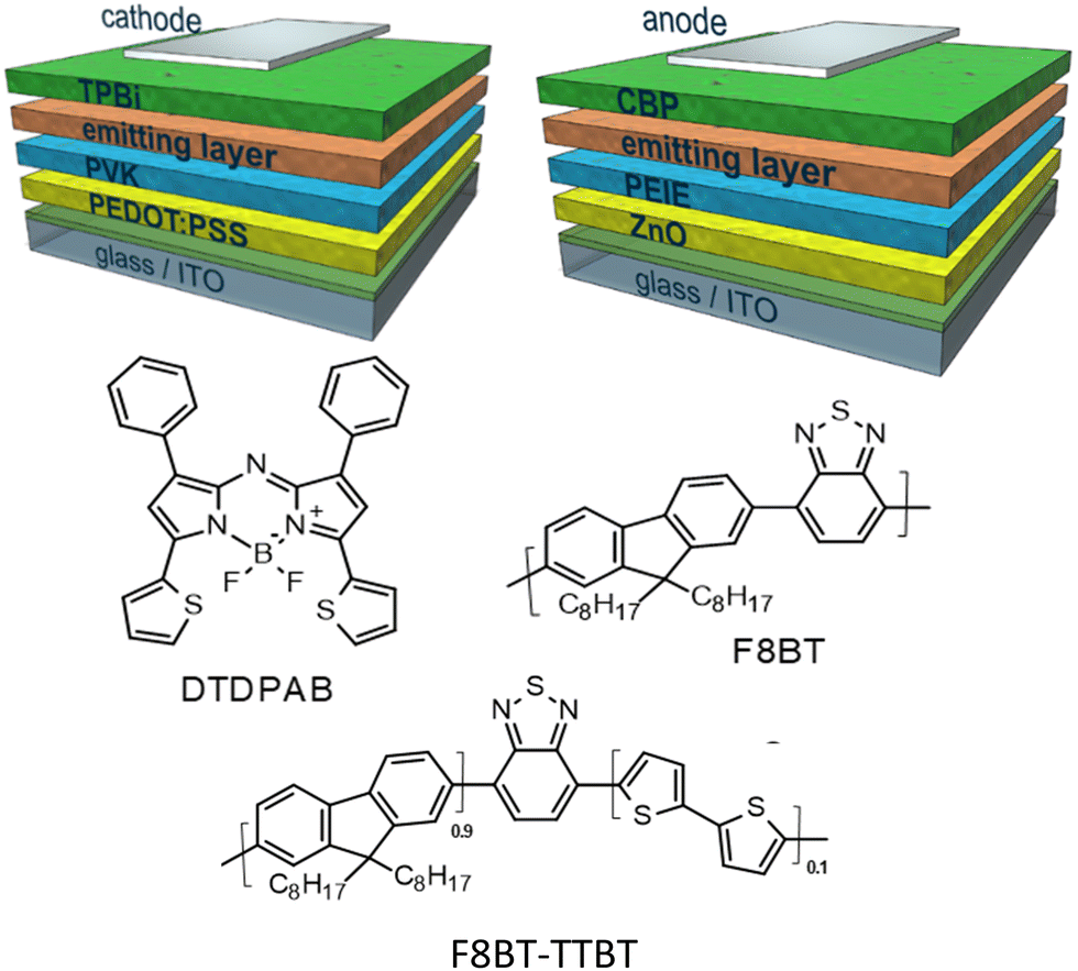 | ||
| Scheme 1 General architectures of direct (left) and inverted (right) diodes used in this work together with structures of the materials applied in the emitting layers. | ||
In rigid planar systems such as BODIPY derivatives, the formation of aggregates is one of the main causes of quenching combined with high nonradiative transition rate due to the energy gap law. In general these materials are dispersed in a host which decreases the aggregation quenching but causes an undesired blue shift of the emission.38,39
In this work we were able to exploit the emission of the aggregate in the real NIR at 910 nm in an OLED. We use the standard approach of dispersing the dye in a host based on the commercial conjugated polymer F8BT and its derivative random copolymer synthesized in our laboratory F8BT-TTBT (see Scheme 1).40 We were able to obtain a delicate balance between the quenching effect of the emission caused by the aggregation and the blue shift of the emission due to the dispersion of the organic molecule. In order to improve the effectiveness of our approach we modified the architecture of the devices, direct and inverted, the charge regulating layers, and the polymeric host. In fact, we have synthesized a new polymer via Suzuki random copolymerization of benzothiadiazole, 9,9-di-octylfluorene and 2,2′-bithiophene derivatives which shifted emission towards red spectral region with respect to standard F8BT in order to modulate energy transfer between the polymeric matrix and the dye. Through this approach we demonstrate that OLEDs spectrum can be adjusted depending on the applicative requirements of the device. By controlling the various parameters, we were able to modulate the emission of the device and finally the electroluminescence of the aggregates at 910 nm was obtained.
Experimental
Synthetic methods
 | ||
| Scheme 2 Synthetic route for DTDPAB molecule. | ||
Devices assembly and characterization
In the case of inverted structure devices, zinc oxide (ZnO) nanocrystals (Avantama, N-10) were diluted in isopropanol solution (from 2.5% to 1.6% wt) and put in ultrasonic bath for 30 minutes. Such prepared solution was spined at 1000 rpm on the cleaned ITO substrates which were treated before deposition with UV-ozone for 1 minute. Afterwards, the substrates were annealed at 120 °C for 20 minutes in air. Next, polyethylenimine, 80% ethoxylated (PEIE, 35–40% wt in water, average Mw ∼ 70![[thin space (1/6-em)]](https://www.rsc.org/images/entities/char_2009.gif) 000, Aldrich) solution in 2-methoxyethanol (3.9 mg ml−1) was spincoated on the ZnO covered substrates at 5000 rpm rotation. Substrates preparation was concluded with 10 minutes annealing at 100 °C.
000, Aldrich) solution in 2-methoxyethanol (3.9 mg ml−1) was spincoated on the ZnO covered substrates at 5000 rpm rotation. Substrates preparation was concluded with 10 minutes annealing at 100 °C.
Two types of emitting layers were employed in direct-driven devices on the PVK covered substrates: (i) 95% F8BT: 5% DTDPAB and (ii) 40% F8BT: 10% F8BT-TTBT: 50% DTDPAB, where F8BT stands for commercially available poly[(9,9-dioctylfluorenyl-2,7-diyl)-alt-co-(1,4-benzo-{2,1′,3}-thiadiazole)] (American Dye Source, ADS133YE), while F8BT-TTBT denotes poly(9,9-dioctylfluorene-alt-benzothiadiazole)(dithienyl-benzothiadiazole) and DTDPAB – dithienyl diphenyl AZABODIPY, both synthesized in our laboratory. The ratio in the recipes is based on weights and the final concentration of the emitting layers’ solutions was 15 mg ml−1. The compounds were dissolved in extra dry toluene and left overnight at 50 °C with stirring. The emitting layers were spined inside nitrogen filled glovebox at 2000 rpm rotation in a case of the first type device and at 800 rpm in the case of the second one. In the case of the second diode, on the emitting layer 35 nm of 1,3,5-tris(1-phenyl-1H-benzimidazol-2-yl)benzene (TPBi, Ontario Chemicals, Inc.) was evaporated with rate 0.2 Å s−1 at 3 × 10⁻⁷ mbar pressure. Finally, cathodes consisting of 7 nm of barium and 100 nm of aluminium were evaporated at 1 × 10⁻⁶ mbar.
In the case of inverted structure diodes, the emitting layers were prepared the same way as in the case of the second direct architecture device. Subsequently, 4,4′-bis(N-carbazolyl)-1,1′-biphenyl (CBP, Sigma-Aldrich) was evaporated with rate 0.2 Å s−1 at 3 × 10⁻⁷ mbar pressure, creating the 35 nm thick hole transporting layers. As anodes either 10 nm thick MoO3 layer covered with 100 nm of aluminium or 50 nm of gold were used. The active area of a single pixel was 6.1 mm2.
In case of hole-only and electron-only devices used for mobility determination, they had structures ITO/PEDOT:PSS/40% F8BT: 10% F8BT-TTBT: 50% DTDPAB/MoO3/Al and ITO/ZnO/PEIE/40% F8BT: 10% F8BT-TTBT: 50% DTDPAB/Ba/Al, respectively. Devices constructed for the charge balance verification had on the top of the emitting layer evaporated CBP layer and the same electrodes and charge injecting layers as for the hole-only and electron-only devices.
Electrochemistry was performed at room temperature in acetonitrile under nitrogen in three electrode cells. The counter electrode was platinum; reference electrode was Ag/Ag+ (0.1 M AgNO3 in acetonitrile, 0.34 V vs. SCE, −4.73 V vs. vacuum), supporting electrolyte was 0.1 M tetrabutylammonium perchlorate (TBAP). Cyclic Voltammetry was performed at a scan rate of 0.1 V s−1. Working electrode was glassy carbon (GC, 0.2 cm2). F8BT, F8BT-TTBT, DTDPAB films were casted onto electrodes at 80–90 °C from 1 mg mL−1 solutions in chloroform (2 mL). The voltammetric apparatus was Metrohm Autolab 128N potentiostat/galvanostat.
Photoluminescence (PL) spectra were obtained with a NanoLog composed by the iH320 spectrograph equipped with the Synapse QExtra charge-coupled device by exciting with a monochromated 450 W Xe lamp. The spectra are corrected for the instrument response. Time-resolved TCSPC measurements were obtained with PPD-850 single photon detector module and DD-405L DeltaDiode Laser and analysed with the instrument Software DAS6.
Results and discussion
Synthesis
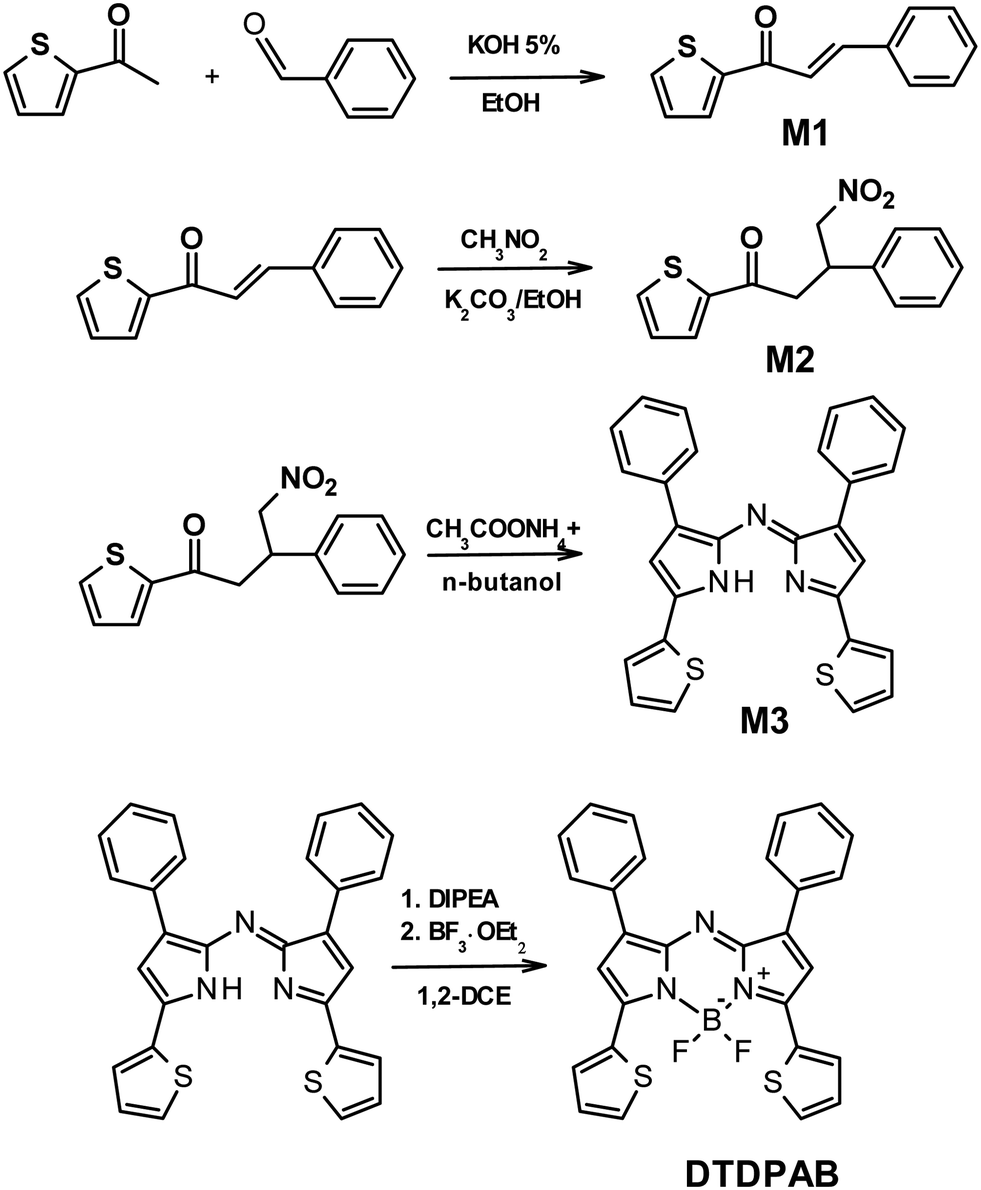
The thienyl substituted AZABODIPY (DTDPAB) is synthetized according to the literature36,37 and described in detail in the experimental section and in Scheme 2. The first step is the synthesis of the chalcone M1 with the condensation of 2-acetylthiophene and benzaldehyde. The intermediate phenyl 4-nitro-3-thienylbutan-1-one M2 is obtained in the second step by reacting the obtained M1 with nitromethane and potassium carbonate. Subsequently M2 is used in the next step without further purification reacting with ammonium acetate to obtain the azadipyrromethene derivative M3. In the last step N,N-diisopropylethylamine with boron trifluoride diethyl etherate react with M3 to give the final product dithieno-diphenyl-aza-BODIPY.The polymeric host F8BT-TTBT (see Scheme 1) is a random tercopolymer synthetized via standard Suzuki polymerization conditions by using toluene as a solvent and Pd(0) as a catalyst. The bithiophene-based monomer responsible for the red shift of the emission has been added in a percentage of 10%. Our previous studies have shown that with these percentages a complete energy transfer in the emission is obtained and the energy levels are comparable with the parent F8BT.9
Optoelectronic and electrochemical properties
In Fig. 1(a) the absorption, PL excitation and PL spectra of DTDPAB in solution are presented. The absorption spectrum displays three main bands peaked at 345 nm, 475 nm and 720 nm. The PL spectrum has a sharp peak at 733 nm with a band, very probably a vibronic replica, at about 800 nm, with excitation spectra closely corresponding to the absorption. The emission properties do not display significant variations with the solvent (see Table S1 and Fig. S5 and S6, ESI†) with PL Quantum Yield of 0.43 and lifetime of 3.3 ns in chloroform. These findings correspond well with the results presented by Zhang et al. in ref. 36. The PL emission is the mirror image of the absorption peaks at the longest wavelengths. The small Stokes shift (30 meV) suggests that the molecule possesses high rigidity and consequently should not dissipate much energy, an important property for a NIR emitter influenced by the energy gap law.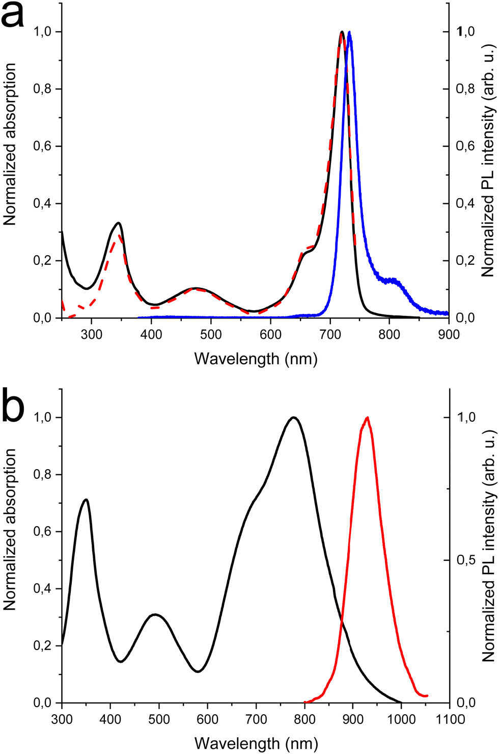 | ||
| Fig. 1 (a) Absorption (black solid), excitation (red dash) and PL (blue solid) spectra of DTDPAB in chloroform (c = 10−5 M), (b) absorption (black solid) and PL (red solid) spectra of DTDPAB cast film. | ||
Fig. 1(b) shows the absorption and PL spectra of DTDPAB in the solid state. With respect to the absorption spectra in solutions, the longest wavelength absorption band of the film displays a large broadening and red-shifts to 777 nm. Accordingly, the PL spectrum is red-shifted to 930 nm. Moreover, the PL intensity is drastically reduced, with a PLQY below the sensitivity of our instrument (0.1%). The PL decay profile (Fig. S7, ESI†) is much faster than in solution, displaying a lifetime of about 300 ps. The PL properties of DTDPAB cast films indicate the presence of efficient emission quenching processes in the solid state, as often observed for organic moieties displaying strong intermolecular interactions upon aggregation in thin films, powders and crystals.41,42
The CVs analyses show that F8BT film presents one irreversible oxidation process at 1.08 V (Fig. S8, Table S2, ESI† and Table 1) which may interest the fluorene moiety. In F8BT-TTBT film the oxidation process splits into two peaks at 1.06 V and 1.13 V (Fig. S9, Table S2, ESI† and Table 1), where the second peak may be ascribed to the bithiophene moiety. Both polymers present one reversible reduction process at comparable potentials which may be due the fluorene moiety. The CV response of DTDPAB in solid-state films results to be more complex than in solution: the oxidation response splits into three peaks at 0.7 V, 0.82 V, and 1.39 V while the two reduction ones become irreversible (Fig. 2, Fig. S10, Table S2, ESI† and Table 1).36 A possible explanation is that the CV response may be severely affected by the solid-state conditions such as different aggregate or amorphous phases.43
| E ox | E red | HOMO | LUMO | E gcv | |
|---|---|---|---|---|---|
| DTDPAB | 0.57 | −0.65 | −5.30 | −4.08 | 1.22 |
| F8BT-TTBT | 0.97 | −1.8 | −5.70 | −2.93 | 2.77 |
| F8BT | 0.99 | −1.84 | −5.72 | −2.89 | 2.83 |
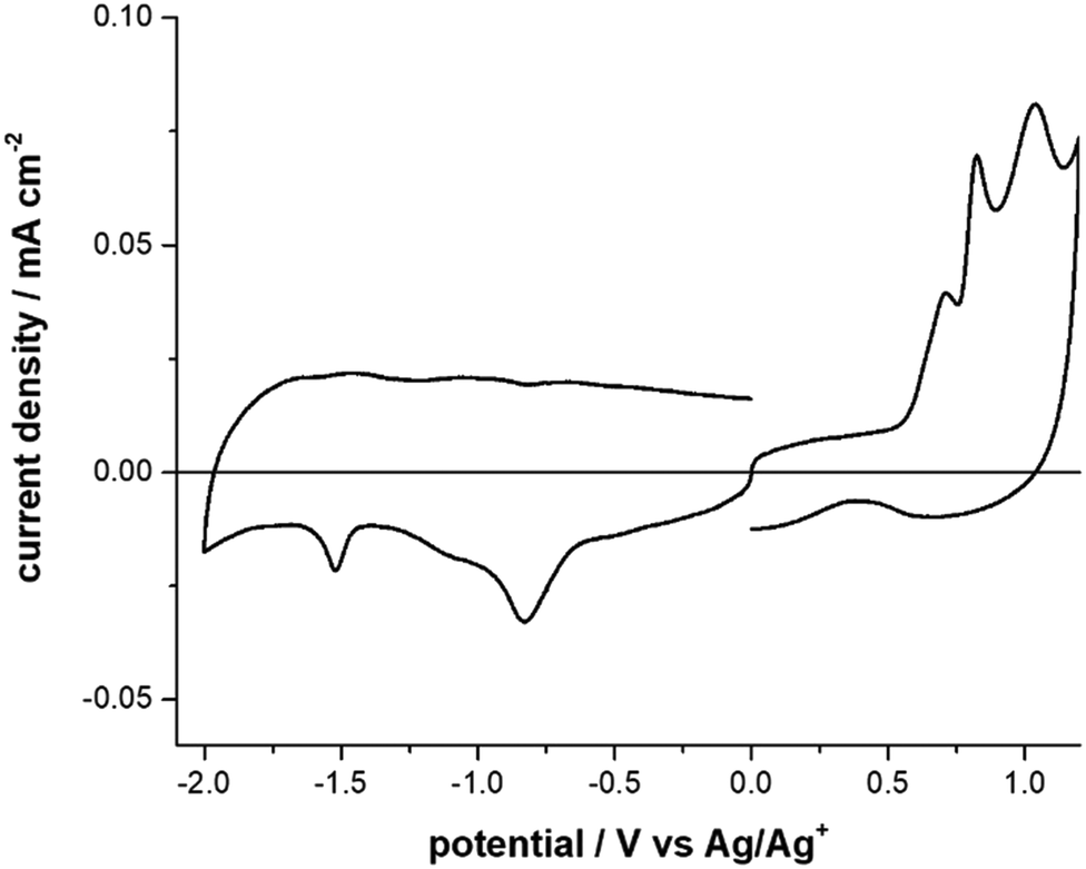 | ||
| Fig. 2 Cyclic Voltammograms of DTDPAB molecule, in acetonitrile + 0.1 M Bu4NClO4. Scan rate: 0.1 V s−1. | ||
The nitrogen atom replacing the carbon atom in the meso position of DTDPAB induces the desired bathochromic shift without increasing molecular size and weight and maintaining good solubility. Compared to the parent BODIPY, the electronegativity of nitrogen induces a preferable stabilization of the LUMO state, reducing the energy gap (see Table S2, ESI†). Contemporarily the electro-donating thiophene substituents increase the HOMO level, while the LUMO level remains nearly constant, resulting in a further reduced energy gap with a bathochromic shift. Furthermore, less steric hindrance of thienyl five-member ring with respect to the six-member phenyl ring allows for greater coplanarity enhancing the electron delocalization.
As regards the polymeric hosts, the main optoelectronic characteristics are shown in Table 1 and Fig. S11 (ESI†). As anticipated, the two polymers have comparable energy levels as expected from the low percentage of the thiophene monomer with respect to the F8BT one. The optical properties of the two polymers differ in an evident way as concerns the emission, in fact F8BT and F8BT-TTBT have the PL at 555 nm and 660 nm, respectively, while in the absorption their spectra are similar with addition of a small band at 550 nm in the case of the polymer with thiophenes.
Electroluminescence performance
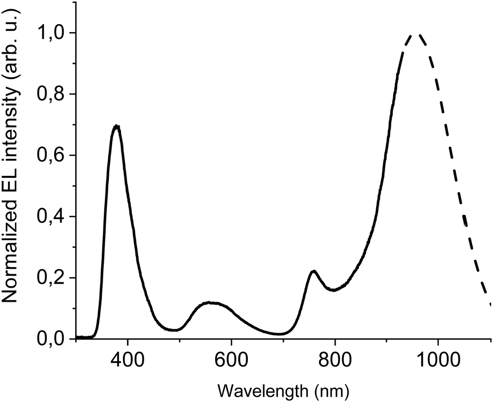
The first device to test DTDPAB abilities as an emitter had simple yet multilayer direct architecture ITO/PEDOT:PSS/PVK/95% F8BT: 5% DTDPAB/Ba/Al. All organic films were deposited by spincoating technique which is cheaper and faster than thermal evaporation processing. High molecular weight PVK deposited on PEDOT:PSS plays a role of hole transporting layer and allows deposition of the emitting layer from solution. Simultaneously, PVK prevents radiative excitons from quenching caused by the acidic nature of PEDOT:PSS.9 Additionally, the shallower LUMO level of PVK (−2.3 eV) with respect to the deeper LUMO of F8BT (−2.89 eV) blocks electrons traveling towards the anode and prevents in this way the leakage current.Fig. 3 presents the EL spectrum of the device. Contributions from F8BT (500–650 nm) and DTDPAB (700–900 nm) to the spectrum are clearly distinguishable and correspond to their PL spectra, while PVK emission is not present in the EL. The F8BT band has a typical form for this polymer, while DTDPAB EL spectrum displays a 30 nm red-shift (the peak at 760 nm and the shoulder at 835 nm) with respect to the PL in solution, revealing intermediate characteristics between the solution and solid state as expected in a blend. Moreover, the long wavelength shoulder in the EL spectrum is more pronounced than in chloroform, probably due to the DTDPAB aggregate emission.
 | ||
| Fig. 3 EL at 100 mA cm−2 of ITO/PEDOT:PSS/PVK/95% F8BT: 5% DTDPAB/Ba/Al direct architecture device. | ||
The presence of F8BT emission in the EL spectrum is the evidence that energy transfer from the host to DTDPAB is not particularly efficient. The cause of this is the poor overlap of the F8BT emission and the guest absorption, as envisaged in Fig. S11 (ESI†).
The results of electrical characterization of the device are shown in Fig. S12 (ESI†) and in Table 2. The turn-on voltage is equal to 8 V and corresponds to the quite high current density of 1.2 × 10⁻⁴ A cm−2. The maximal recorded radiance is equal to moderate 0.58 W sr−1 m−2 which in combination with high current densities gives as a result modest maximal EQE of 0.04%.
| Structure | Peak wavelength (nm) | EQEmax (%) | EL in NIR (>700 nm %) |
|---|---|---|---|
| ITO/PEDOT:PSS/PVK/95% F8BT: 5% DTDPAB/Ba/Al | 550, 760 | 0.0413 | 89 |
| ITO/PEDOT:PSS/PVK/40% F8BT: 10% F8BT-TTBT: 50% DTDPAB/TPBi/Ba/Al | 378, 550, 758, >900 | 0.0090 | 75 |
| ITO/ZnO/PEIE/40% F8BT: 10% F8BT-TTBT: 50% DTDPAB/CBP/MoO3/Al | >900 | 0.0018 | 100 |
| ITO/ZnO/PEIE/40% F8BT: 10% F8BT-TTBT: 50% DTDPAB/CBP/Au | 785, 910 | 0.0027 | 100 |
Intrigued by the DTDPAB spectrum, we built a device with highly concentrated guest molecule to determine if the emission can be further shifted towards NIR spectral region. In Fig. S13 (ESI†), the EL spectrum of the diode with emitting layer (EML) consisting of 80% DTDPAB in F8BT matrix is presented. The spectrum is dominated by a broad band centred at 950 nm with a peak at 760 nm originating from single DTDPAB molecules, however, the F8BT band is still visible. The EQE of the device decreased one order of magnitude in comparison to the diode with low guest concentration due to the concentration quenching44 (Fig. S14, ESI†).
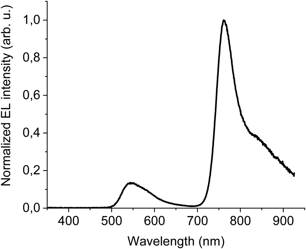
In order to improve the efficiency, we decided to add F8BT-TTBT polymer to the emissive layer's components and at the same time to decrease concentration of DTDPAB to 50%. The task of the new polymer is to improve energy transfer from the matrix to the guest molecules thanks to the better overlap of their spectra (Fig. S11, ESI†). The decreased emitter concentration should diminish concentration quenching. Finally, we introduced thermally evaporated TPBi as an electron transporting layer (ETL) to separate recombination zone from the cathode and to avoid in this way plasmon creation in the electrode. TPBi should also block a leakage current of holes thanks to the deep HOMO level45 (see Fig. 4(a)). EL spectrum of this new diode is shown in Fig. 5.
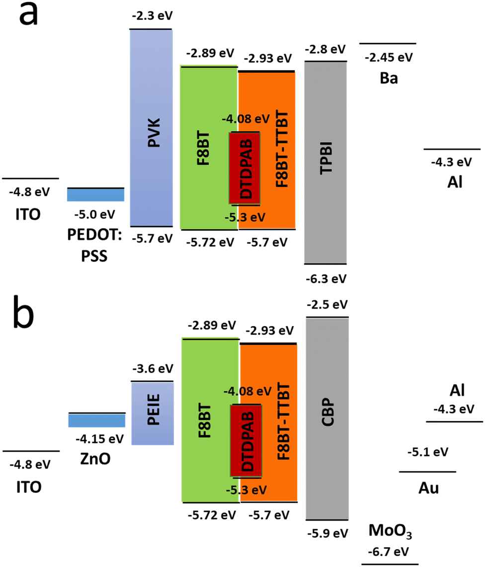 | ||
| Fig. 4 Energy levels of all materials employed in the direct (a) and inverted (b) devices. For the configuration of a specific diode see text. | ||
 | ||
| Fig. 5 EL at 100 mA cm−2 of ITO/PEDOT:PSS/PVK/40% F8BT: 10% F8BT-TTBT: 50% DTDPAB/TPBi/Ba/Al device. Dashed line shows simulated extrapolation of the spectrum. | ||
The emission of the DTDPAB molecule is better resolved than in the previous cases but resembles earlier registered EL spectra, the F8BT band is also visible. On the other hand, the EL from F8BT-TTBT is not present which suggests successful energy transfer from the polymer to the dopant. The confirmation of this process is presented in Fig. S15 (ESI†), where a device with the emitting layer composed of 80% F8BT: 20% F8BT-TTBT (the same hosts ratio as in the device in Fig. 5 but without DTDPAB) shows electroluminescence solely from F8BT-TTBT. Therefore, energy transfer together with the dopant concentration adjustment creates the possibility of spectrum control depending on the particular application needs: when simultaneous emission in visible and NIR is required, a non-transferring matrix can be used while for pure NIR emission polymer with good overlap with the acceptor should be applied.
The new band in the EL spectrum in the UV-blue region is associated with TPBi electroluminescence.46 This emission cannot originate from PVK since the LEDs with this polymer but without TPBi layer do not emit in this spectral range (see Fig. 3 and Fig. S13, ESI†) and also the PVK electroluminescence is placed at longer wavelengths (Fig. S16, ESI†). The EQE of the device is equal to 0.009% (Fig. S17, ESI†), which is higher than for the diode without F8BT-TTBT and TPBi (EQE = 0.003%) but lower than for the LED with low DTDPAB concentration. It is reasonable to assume that big contribution of TPBi and the polymers to the total emission had influence on the EQE of the device. Turn-on voltage increased to 10 V due to a higher thickness of the device. Since we were interested in pure NIR emission, changes in the diode design were necessary. Visible TPBi EL is clear evidence that the recombination zone is at the EML/ETL interface. In order to avoid emission from the transporting layer we decided to apply an inverted architecture in the form ITO/ZnO/PEIE/40% F8BT: 10% F8BT-TTBT: 50% DTDPAB/CBP/MoO3/Al. The EL spectrum of the device is shown in Fig. S18 (ESI†) and is purely in the NIR spectral region (>700 nm) which may suggest that the recombination zone was moved towards PEIE/EML interface. However, the maximal EQE of the diode decreased to 0.0018% (Fig. S19, ESI†). Suspecting that this drop in the EQE may be caused by too facile injection of holes thanks to the deep laying MoO3 energy level (see Fig. 4(b)) we substituted this anode with a gold electrode. As a result, the maximal EQE increased to 0.0027% preserving at the same time purely NIR emission with the maximum at 910 nm (Fig. S20, ESI† and Fig. 6, respectively).
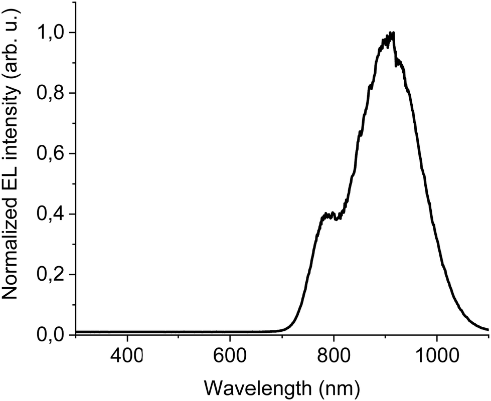 | ||
| Fig. 6 EL at 100 mA cm−2 of ITO/ZnO/PEIE/40% F8BT: 10% F8BT-TTBT: 50% DTDPAB/CBP/Au inverted architecture device. | ||
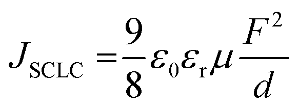
To understand better the origin of the low EQE values, we built and characterized electron-only and hole-only devices with the EML layer. Subsequently, we extracted electron and hole mobilities in the emitting layer, applying the Mott–Gurney law for the field range where the currents were limited by a space charge (SCLC),
Conclusions
Organic emitters play a role of increasing interest thanks to the multiple fields of application. However, to obtain materials capable of efficient emission in the deep infrared region (over 850 nm) has proved to be an unresolved challenge for chemists.In fact, to realize an emitter with these characteristics, the difference between the HOMO–LUMO energy levels must be lower than 1.46 eV and this often leads to a low air stability. Moreover, these materials being generally formed by planar conjugate systems, easily aggregate suffering from aggregation quenching which combined with the energy gap law are the main limitations to obtain the objective. On the other hand, the possibility of getting emissive aggregates from smaller molecules can lead to a simplification of the synthesis with respect to large conjugated structures.
In the present work we were able to obtain emissive aggregates of the AZABODIPY derivative and this allowed to red shift the maximum emission from 733 nm in solution, to 760 nm in the blend without aggregates and up to 930 nm in the case of emissive aggregates. A further important result was the electroluminescence achieved from these clusters. Through the study of the geometry of the device, direct and inverted, the use of charge regulating layers, and the choice of suitable polymeric hosts, a pure emission in NIR with the maximum at 910 nm was obtained. Up to our knowledge, this is the first example of electrically excited single AZABODIPY emitter that emits in real NIR (>700 nm).
This result is a proof of concept that paves the way for the development and application of AZABODIPYs as electroluminescent emitters in NIR. Furthermore, the approach introduced in the present work can be a valid suggestion to deepen the study of other already known materials that could show the same type of behaviour.
Author contributions
B. M. S. synthesized the materials, interpreted NMR spectra and with B. V. performed electrochemical characterization, C. B. measured photophysical properties, W. M. fabricated and characterized the devices, M. P. supervised the work. All authors contributed to the data analysis, discussed the results, and contributed to the writing of the manuscript.Conflicts of interest
There are no conflicts to declare.References
- G. Qian and Z. Y. Wang, Chem. – Asian J., 2010, 5, 1006–1029 CrossRef CAS PubMed.
- A. Zampetti, A. Minotto and F. Cacialli, Adv. Funct. Mater., 2019, 29, 1807623 CrossRef.
- J. H. Kim, J. H. Yun and J. Y. Lee, Adv. Opt. Mater., 2018, 6, 1800255 CrossRef.
- J. Zhang, H. Ye, Y. Jin and D. Han, Top. Curr. Chem., 2022, 380, 1–40 CrossRef PubMed.
- Y. Liu, Y. Chen, H. Li, S. Wang, X. Wu, H. Tong and L. Wang, ACS Appl. Mater. Interfaces, 2020, 12, 30652–30658 CrossRef CAS PubMed.
- C. Zang, S. Liu, M. Xu, R. Wang, C. Cao, Z. Zhu, J. Zhang, H. Wang, L. Zhang, W. Xie and C.-S. Lee, Light: Sci. Appl., 2021, 10, 116 CrossRef CAS PubMed.
- S. Kesarkar, W. Mróz, M. Penconi, M. Pasini, S. Destri, M. Cazzaniga, D. Ceresoli, P. R. Mussini, C. Baldoli, U. Giovanella and A. Bossi, Angew. Chem., Int. Ed., 2016, 55, 2714–2718 CrossRef CAS PubMed.
- F. Li, A. J. Gillett, Q. Gu, J. Ding, Z. Chen, T. J. H. Hele, W. K. Myers, R. H. Friend and E. W. Evans, Nat. Commun., 2022, 13, 2744 CrossRef CAS PubMed.
- U. Giovanella, P. Betti, A. Bolognesi, S. Destri, M. Melucci, M. Pasini, W. Porzio and C. Botta, Org. Electron., 2010, 11, 2012–2018 CrossRef CAS.
- C. W. Tang and S. A. VanSlyke, Appl. Phys. Lett., 1987, 51, 913–915 CrossRef CAS.
- S. R. Forrest, Nanophotonics, 2021, 10, 31–40 CAS.
- Q. Wei, N. Fei, A. Islam, T. Lei, L. Hong, R. Peng, X. Fan, L. Chen, P. Gao and Z. Ge, Adv. Opt. Mater., 2018, 6, 1800512 CrossRef.
- G. Hong, X. Gan, C. Leonhardt, Z. Zhang, J. Seibert, J. M. Busch and S. Bräse, Adv. Mater., 2021, 33, 2005630 CrossRef CAS PubMed.
- U. Giovanella, M. Pasini and C. Botta, in Applied Photochemistry: When Light Meets Molecules, ed. G. Bergamini and S. Silvi, Cham, Switzerland, 2016, vol. 92, pp.145–196 Search PubMed.
- Y.-C. Wei, S. F. Wang, Y. Hu, L.-S. Liao, D.-G. Chen, K.-H. Chang, C.-W. Wang, S.-H. Liu, W.-H. Chan, J.-L. Liao, W.-Y. Hung, T.-H. Wang, P.-T. Chen, H.-F. Hsu, Y. Chi and P.-T. Chou, Nat. Photonics, 2020, 14, 570–577 CrossRef CAS.
- Y. Xie, W. Liu, W. Deng, H. Wu, W. Wang, Y. Si, X. Zhan, C. Gao, X.-K. Chen, H. Wu, J. Peng and Y. Cao, Nat. Photon., 2022, 16, 752–761 CrossRef CAS.
- J. Royakkers, A. Minotto, D. G. Congrave, W. Zeng, A. Hassan, A. Leventis, F. Cacialli and H. Bronstein, Chem. Mater., 2020, 32, 10140–10145 CrossRef CAS.
- A. Minotto, P. A. Haigh, G. Łukasiewicz, E. Lunedei, D. T. Gryko, I. Darwazeh and F. Cacialli, Light: Sci. Appl., 2020, 9, 70 CrossRef PubMed.
- A. Minotto, I. Bulut, A. G. Rapidis, G. Carnicella, M. Patrini, E. Lunedei, H. L. Anderson and F. Cacialli, Light: Sci. Appl., 2021, 10, 18 CrossRef CAS PubMed.
- K. Guo, M. Righetto, A. Minotto, A. Zampetti and F. Cacialli, iScience, 2021, 24, 102545 CrossRef CAS PubMed.
- Z. Liu, Z. Jiang, M. Yan and X. Wang, Front. Chem., 2019, 7, 712 CrossRef CAS PubMed.
- A. Loudet and K. Burgess, Chem. Rev., 2007, 107, 4891–4932 CrossRef CAS PubMed.
- B. M. Squeo, V. G. Gregou, A. Avgeropoulos, S. Baysec, A. Sybille, S. Ullrich and C. L. Chochos, Prog. Polym. Sci., 2017, 71, 26–52 CrossRef CAS.
- B. M. Squeo and M. Pasini, Supramol. Chem., 2020, 32, 56–70 CrossRef CAS.
- M. Poddar and R. Misra, Coord. Chem. Rev., 2020, 421, 213462 CrossRef CAS.
- R. G. Clarke and M. J. Hall, in Advances in Heterocyclic Chemistry, ed. E. F. V. Scriven and C. A. Ramsden, Academic Press, 2019, vol. 128, pp.181–261 Search PubMed.
- J. Killoran, L. Allen, J. F. Gallagher, W. M. Gallagher and D. F. O’Shea, Chem. Commun., 2002, 1862–1863 RSC.
- D. Wu, S. Cheung, G. Sampedro, Z.-L. Chen, R. A. Cahill and D. F. O’Shea, Biochim. Biophys. Acta, Biomembr., 2018, 1860, 2272–2280 CrossRef CAS PubMed.
- N. Adarsh, P. S. Saneesh Babu, R. R. Avirah, M. Viji, S. A. Nair and D. Ramaiah, J. Mater. Chem. B, 2019, 7, 2372–2377 RSC.
- Y. Kage, S. Kang, S. Mori, M. Mamada, C. Adachi, D. Kim, H. Furuta and S. Shimizu, Chem. – Eur. J., 2021, 27, 5259–5267 CrossRef CAS PubMed.
- A. Zampetti, A. Minotto, B. M. Squeo, V. G. Gregoriou, S. Allard, U. Scherf, C. L. Chochos and F. Cacialli, Sci. Rep., 2017, 7, 1611 CrossRef PubMed.
- A. Aguiar, J. Farinhas, W. da Silva, I. C. Santos, L. Alcácer, C. M. A. Brett, J. Morgado and A. J. F. N. Sobral, Dyes Pigm., 2021, 193, 109517 CrossRef CAS.
- K. Ivaniuk, A Pidluzhna, P. Stakhira, G. V. Baryshnikov, Y. P. Kovtun, Z. Hotra, B. F. Minaev and H. Ågren, Dyes Pigm., 2020, 175, 108123 CrossRef CAS.
- M. Shikano, M. Morimoto and S. Naka, Org. Electron., 2021, 99, 106320 CrossRef CAS.
- C. Yang, J. H. Lee and C. Chen, J. Chin. Chem. Soc., 2019, 66, 1199 CrossRef CAS.
- X. Zhang, H. Yu and Y. Xiao, J. Org. Chem., 2012, 77, 669–673 CrossRef CAS PubMed.
- R. Gresser, H. Hartmann, M. Wrackmeyer, K. Leo and M. Riede, Tetrahedron, 2011, 67, 7148–7155 CrossRef CAS.
- C. Li, R. Duan, B. Liang, G. Han, S. Wang, K. Ye, Y. Liu, Y. Yi and Y. Wang, Angew. Chem., Int. Ed., 2017, 56, 11525–11529 CrossRef CAS PubMed.
- C. Du, Z. Cheng, A. Shang, Y. Xu, A. Berlin, C. Lei, Y. Chang, Y. Lv and P. Lu, Chem. Eng. J., 2022, 435, 135010 CrossRef CAS.
- T. Virgili, L. Ganzer, C. Botta, B. M. Squeo and M. Pasini, Molecules, 2022, 27, 4538 CrossRef CAS PubMed.
- C. Botta, G. Patrinoiu, P. Picouet, S. Yunus, J.-E. Communal, F. Cordella, F. Quochi, A. Mura, G. Bongiovanni, M. Pasini, S. Destri and G. Di Silvestro, Adv. Mater., 2004, 16, 1716–1721 CrossRef CAS.
- J. Gierschner, J. Shi, B. Milián-Medina, D. Roca-Sanjuán, S. Varghese and S. Park, Adv. Opt. Mater., 2021, 9, 2002251 CrossRef CAS.
- M. Pasini, B. Vercelli, G. Zotti and A. Berlin, Electrochim. Acta, 2016, 193, 261–267 CrossRef CAS.
- J. B. Birks, Photophysics of aromatic molecules, Wiley-Interscience, London, New York, 1970 Search PubMed.
- X. Jiang, Z. Zhang, W. Zhao, W. Zhu, B. Zhang and S. Xu, J. Phys. D: Appl. Phys., 2000, 33, 473–476 CrossRef CAS.
- N. B. Kotadiya, H. Lu, A. Mondal, Y. Ie, D. Andrienko, P. W. M. Blom and G.-J. A. H. Wetzelaer, Nat. Mater., 2018, 17, 329–334 CrossRef CAS PubMed.
Footnotes |
| † Electronic supplementary information (ESI) available: Synthesis routes, NMR spectra, optical and electrochemical properties and devices characterization data. See DOI: https://doi.org/10.1039/d3ma00006k |
| ‡ These authors contributed equally. |
| This journal is © The Royal Society of Chemistry 2023 |