
 Open Access Article
 This Open Access Article is licensed under a
 Creative Commons Attribution 3.0 Unported Licence
1D aligned, n–p and n–n type ZnO heterojunction nanofibers for NO2 sensors: exploration of conduction mechanism using in situ impedance spectroscopy†
Ramakrishnan
Vishnuraj
,
Mahaboobbatcha
Aleem
,
Keerthi G
Nair
and
Biji
Pullithadathil
 *
*
Nanosensor Laboratory, Department of Chemistry & Nanoscience and Technology, PSG Institute of Advanced Studies, Coimbatore–641 004, India. E-mail: bijuja123@yahoo.co.in; pbm@psgias.ac.in
First published on 8th June 2023
Abstract
Highly aligned 1D n–p type ZnO/Bi2O3 and n–n type ZnO/In2O3 heterojunction nanofibers (HNFs) have been developed using coaxial electrospinning approach, aiming at exploring the effect of 1D aligned heterojunction nanofibrous structure on their NO2 sensing properties. The aligned HNFs have been structurally and morphologically characterized using various spectroscopic and microscopic analyses. The n–p heterojunctions of ZnO/Bi2O3 NFs and n–n heterojunctions of ZnO/In2O3 NFs exhibited significantly boosted sensitivity towards NO2 compared to pristine ZnO NFs. The superior responses of ZnO/Bi2O3 and ZnO/In2O3 HNFs have been attributed to their unique electron transport properties originated from work function differences, leading to the formation of interfacial accumulation and depletion of electrons resulting in surface band bending. The charge depletion of Bi2O3/ZnO HNFs was estimated to be higher due to the interaction of NO2 gas at an operating temperature of 300 °C, resulting in quick response time (8–10 s) and 10 times superior sensitivity than ZnO NFs. Whereas, n-In2O3/n-ZnO HNFs-based sensor exhibited a reduced operating temperature (200 °C) with superior sensitivity (S ∼ 340%), rapid response (5–7 s) with minimal interference towards exposure to trace-level NO2 (500 ppb). The complex sensing mechanisms associated with n–p/n–n type HNFs have been deduced using in situ AC impedance spectroscopic studies, which endorsed the contributions from the modulation of grain and grain boundary resistance and charge transfer between n–p and n–n type materials. The results suggest that the boosted gas sensing properties of aligned 1D n–p and n–n type HNFs under atmospheric pressure conditions can pave the way for development of inexpensive and highly sensitive NO2 gas sensors.
1. Introduction
Owing to the rapid expansion of automobiles and industries, environmental pollution arising from the emissions of hazardous nitrogen dioxide (NO2) causes severe ecological deprivation posing serious threats to human health.1,2 Although various sensors based on metal oxide semiconductors (MOS) and composites have been deployed for sensing NO2 for environmental monitoring applications, sensitivity and selectivity were found to be challenging, especially during trace level detection.3 Among various MOSs, ZnO-based gas sensors were extensively studied owing to the unique physicochemical properties.4–6 Recently, various surface engineered strategies for MOS-based heterojunction materials have been explored for imparting superior response and selectivity towards trace-level detection of NO2.7–10 Pursuant to the nature of semiconductors, formation of n–p and n–n type modifications of MOS can be considered as an efficacy behind enhanced NO2 sensor performance.11,12 Typically, MOS heterojunctions are electrically connected through Fermi level (EF) alignment, i.e., electrons transfer from higher energy state to the lower energy state until the Fermi level achieves equilibrium, which develops a depletion layer at the interface.13 Eventually, potential barriers will be formed across the interface due to band bending.14 Consequently, electrons accumulate at one interface in n–p and n–n heterojunctions leading to an increase in the electron density in the systems.15,16 However, the charge carriers get depleted at the opposite side of the heterojunction interface, which could overcome the potential barrier and further transfer the electrons to interacting gas molecules. Among various types of heterojunction materials, dual MOS type heterojunction interfaces are most suitable for detailed understanding about NO2 detection mechanisms. Although many reports in the literature have attempted to explore the significance of n–p and n–n type structural modifications towards enhancement in NO2 sensor response and selectivity under reduced operating temperature, a concrete understanding of complex sensing mechanism focusing on quantitative contributions of p- and n-type heterojunctions on MOS is not yet available.Among various morphologies, one-dimensional (1D) heterojunction nanostructures have exhibited desirable properties such as high aspect ratio and large surface area leading to elevated gas-sensing properties, which have been found to be more suitable for device integration.17–22 Moreover, in the case of 1D heterojunction MOS materials, the radial modulation of the hole-accumulation layer (HAL) is intensified for shell materials thinner than the Debye length.23 In contrast, the contribution of volume fraction to resistance modulation is found to be weakened. Therefore, modulation of heterojunction morphological arrangement has to be seriously considered when designing a heterojunction MOS-based sensing material, since the NO2 adsorption process fully depends on the surface anchored p- or n-type heterojunctions. Recently, Kim et al. explored the significance of expansion of the HAL in n–p type SnO2–Cu2O core–shell nanowire during NO2 sensing performances.24 It was revealed that the NO2 response deteriorated for SnO2–Cu2O owing to the existence of a thicker Cu2O shell layer, while an increase in the p-layer is restricted by the presence of p–n interface, which act as a blocking layer at the SnO2 sites. In the case of n–n heterojunction materials, Sun et al. explored the NO2 gas sensing characteristics of n-CaO/n-ZnO nanorods, which showed improved sensing performance.25 This is mostly due to the higher variation in barrier potential near the n-CaO/n-ZnO heterojunction during exposure to NO2.
In general, the chemiresistive gas sensing mechanism is purely based on the variations in electrical resistance of a MOS upon gas exposure, which is induced by gas–solid interactions.26,27 The formation of potential barrier energy at the inter-particle interfaces could have the nature of Schottky conduction. However, the conduction mechanism in n–p and n–n type MOS heterojunction materials during charge transfer is still unclear and also a comprehensive understanding of the Schottky barrier formation mechanism in such hybrid materials is crucial for development of superior gas sensor devices. Various in situ techniques have been used to investigate the gas sensing mechanism mediated by charge transfer process, intrinsic defects etc. in various heterojunction nanostructures.28–35In situ alternating current (AC) impedance spectroscopy is a promising and most sensitive technique, which is capable of characterizing the physicochemical processes and of revealing the conduction mechanisms in heterojunction MOSs during gas exposure.36 Generally, direct current (DC) measurements can provide information on device performance such as sensitivity, selectivity and response time. Whereas, AC-based impedance measurements help to categorize and quantify the specific properties responsible for enhanced sensor performances like bulk grain properties, grain boundary properties and interfacial properties of transducers and active sensing regions.37 Impedance spectroscopy can also be used to estimate the donor concentration and depletion region width, in addition to the relative contributions of interfacial and bulk mechanisms towards total conductivity of materials as a function of the working temperature and gas atmosphere.38 Recently, Maziarz et al. investigated the effect of n–n (SnO2–TiO2) and p–n (CuO–TiO2) heterostructured nanolayers on NO2 detection.11 Based on impedance analysis, improved NO2 detection characteristics of the n-SnO2/n-TiO2 heterostructures was attributed to formation of heterointerfaces and larger surface-to-volume ratio. Nevertheless, n-TiO2/p-CuO heterostructures exhibited reduced NO2 responses, which might be ascribed to the effect of charge compensation. Also, Wang et al. performed in situ AC impedance analysis for NiO–WO3 nanorods before and after H2S exposure and revealed that the grain–grain boundary interaction along with p–n junction contributing effect could be the reason behind the superior sensing performance.39 So far, a quantitative approach to unveil the complex sensing phenomenon associated with heterojunction materials during NO2 exposure has not yet been reported.
In this investigation, an on-chip fabrication strategy for creating 1D aligned n–p ZnO/Bi2O3 and n–n ZnO/In2O3 HNFs has been developed based on coaxial electrospinning for NO2 gas sensor applications. The effect of n–p and n–n contributions and nano-grain–grain boundary interactions of the materials during NO2 exposure was investigated by in situ AC impedance spectroscopic studies. This study can contribute significantly towards selection of appropriate surface engineering approaches and process conditions for fabrication of high-performance low-cost aligned heterojunction nanowire sensor devices.
2. Experimental section
Materials
Zinc acetate (98%, Merck), bismuth nitrate pentahydrate (99.8%, Merck), indium chloride (99.7%, Sigma-Aldrich), polyvinyl alcohol (MW: 130![[thin space (1/6-em)]](https://www.rsc.org/images/entities/char_2009.gif) 000, Sigma-Aldrich), polyvinyl pyrrolidone (MW: 200000, Sigma-Aldrich), copper foil, ethanol (Merck) and N,N-dimethylformamide (DMF; Merck) were used without any further purification. Deionized (Type-I) water was used for all synthesis. All the reagents involved in the experiments were of analytical grade and were directly used without further purification.
000, Sigma-Aldrich), polyvinyl pyrrolidone (MW: 200000, Sigma-Aldrich), copper foil, ethanol (Merck) and N,N-dimethylformamide (DMF; Merck) were used without any further purification. Deionized (Type-I) water was used for all synthesis. All the reagents involved in the experiments were of analytical grade and were directly used without further purification.
Method
An in-house electrospinning unit with independently controlled dual syringe pump (HOLMARC) was used to synthesize MOS HNFs using coaxial electrospinning. A DC power supply of 30 kV (Glassman) was utilized in this system. A Teflon-based coaxial spinneret was used for coaxial electrospinning of the materials. 1D aligned coaxial type n-ZnO/p-Bi2O3 and n-ZnO/n-In2O3 HNFs were developed using a coaxial electrospinning process. The in-house built coaxial electrospinning set-up was equipped with independently controlled dual syringe pump for feed fluid supply, coaxial spinneret assembly with concentric nozzles and parallel type copper collector plate.In this typical process, feed solution A was prepared by dissolving 1.2 g zinc acetate in 8 wt% of PVA (polyvinyl alcohol) dissolved in a binary solution containing 10 mL deionized water and 2.5 mL ethanol. After continuous stirring at 60 °C for 3 h, a homogeneous feed solution A was obtained. For preparing feed solution B, 0.2 wt% Bi(NO3) solution and 10 wt% of PVP (polyvinyl pyrrolidone) dissolved in 10 mL DMF were mixed to obtain a viscous solution. The pale white solution was immediately stirred for 2 h. Feed solution C was prepared by stirring a mixture of 0.5 wt% InCl2 solution and 12 wt% of PVP in 10 mL DMF for 4 h to obtain a viscous solution.
2.1. Synthesis of 1D aligned n-ZnO/p-Bi2O3 HNFs
1D aligned n-ZnO/p-Bi2O3 HNFs were fabricated by coaxial electrospinning method. The inner fluid (solution A) was taken as core liquid and the outer shell was taken as solution B. The prepared precursor solution was then transferred into plastic syringes for electrospinning. The precursors were coaxially electrospun from a stainless-steel needle (21 gauge for inner fluid and 18G for outer fluid) attached to the coaxial spinneret assembly. Specifically, the feed rates of inner-core and outer-shell solutions were fixed as 0.4 mL h−1 and 1 mL h−1, respectively, which were controlled using a dual syringe pump. DC voltage of 18 kV was supplied between the needle and collector which was kept at a distance of 21 cm for electrospinning.2.2. Synthesis of 1D aligned n-ZnO/n-In2O3 HNFs
As shown in Scheme 1, the n-ZnO/n-In2O3 NFs were fabricated by the coaxial electrospinning method. Solution A and solution C were taken as the inner-core and outer-shell fluids respectively. The precursors were coaxially electrospun using stainless-steel needles (22G for inner fluid and 19G for outer fluid) attached to the coaxial spinneret assembly. The fluid speeds of inner-core and outer-shell solutions were fixed as 0.8 mL h−1 and 1 mL h−1 respectively, which were further controlled using a dual syringe pump. In this experiment, a 20 kV DC voltage was applied to the needle and the collector (separated with a distance of 18 cm) for electrospinning. As-electrospun core–shell samples of Zn(CH3COO)/PVA/core-PVP/Bi(NO3) shell and Zn(CH3COO)/PVA/core-PVP/InCl2 shell composites were further calcined at 550 °C for 3 h under oxygen environment using a tubular controlled atmosphere furnace with a heating rate of 5 °C min−1 to obtain crystalline n-ZnO/p-Bi2O3 and n-ZnO/n-In2O3 HNFs. | ||
| Scheme 1 Schematic illustration of coaxial electrospinning of aligned ZnO/Bi2O3 and ZnO/In2O3 HNFs. | ||
2.3. In situ AC impedance spectroscopic studies
In situ AC impedimetric studies were performed in order to explore the grain–grain boundary mediated conduction mechanism of 1D n-ZnO/p-Bi2O3 and n-ZnO/n-In2O3 HNFs under air and NO2 atmospheres. The heterojunction sensor was installed on the heating stage inside a custom-made gas sensor test station in our laboratory, which is connected with a Eurotherm temperature controller. The impedance spectra were acquired using a CHI600E electrochemical workstation (CH Instruments, Inc., USA). A constant 100 sccm of NO2 was purged under dynamic state with nitrogen as carrier. An initial voltage of 0.5 V with an amplitude of 0.06 V and frequency range up to 10 MHz was used for all the experiments in order to acquire Nyquist plots.3. Results and discussion
Highly aligned 1D n-ZnO/p-Bi2O3 and n-ZnO/n-In2O3 heterostructured nanofibers were directly spun onto IDA microelectrodes using the coaxial electrospinning method (Fig. S1(a and b), ESI†) and later annealed at 550 °C as depicted in Scheme 1. The heterostructured NFs were aligned transversely on the IDA fingers following the field of electric lines as evidenced by simulations as reported in our previous work.40 During thermal oxidation, polymeric template was decomposed with formation of p-type Bi2O3 and n-type In2O3 nanoislands anchored on wurtzite ZnO nanofibers forming n–p and n–n type heterojunction interfaces, respectively, which were obtained as porous nanofibers. Fig. S1(d and e) (ESI†) presents electron microscopic images of 1D aligned ZnO-based HNFs deposited on an IDA chip before the annealing process. The as-obtained NFs were observed to be highly aligned and of more than a few micrometers in length which are suitable for electronics and sensor applications. Further, from AFM topographic data depicted in Fig. S1(f) (ESI†), HNFs possessed a 1D nanograined structure after annealing.3.1. Structural analysis of ZnO/Bi2O3 and ZnO/In2O3 HNFs
The crystal structures of pristine ZnO, ZnO/Bi2O3 and ZnO/In2O3 HNFs were studied using powder XRD as depicted in Fig. 1(a). Highly intense peaks appeared at 2θ values of 31.697°, 34.325°, 36.357°, 47.416°, 56.507°, 62.769°, 67.867° and 69.6° corresponding to the hexagonal wurtzite structure of ZnO along the crystal planes of (100), (002), (101), (102), (110), (103), (112), and (201), respectively, which are well matched with JCPDS PDF no. 36-1451 for pristine ZnO nanofibers.41Fig. 1(a) depicts the diffraction peaks of n-ZnO/p-Bi2O3 NFs, signifying the existence of heterojunctions and structural purity of the NFs. The coexistence of the peaks indicates the formation of Bi2O3 nanoislands (NIs) along with characteristic ZnO peaks such as (002), (102), (202), (130), (221) and (321) which confirmed that the Bi2O3 NIs exhibited α-Bi2O3 monoclinic structure as inferred from JCPDS no. 71-0465. No further peaks or peak shift were detected in the case of porous, nanograined n-ZnO/p-Bi2O3 NFs confirming the anchoring of p-Bi2O3 NIs onto the ZnO NFs.42 Whereas, in the case of n-ZnO/n-In2O3 HNFs, along with wurtzite ZnO lattice planes, the occurrence of (012), (104), (110), (332), (431) (440), (541) and (217) lattice planes confirmed the formation of heterointerface of In2O3 NIs with rhombohedral structure as inferred from JCPDS no. 73-1809. It is also evident from Fig. 1(a) that no peak shift was observed and thereby no interstitial doping of In2O3 in ZnO occurred while forming nanofibers by coaxial spinning approach while forming the core–shell structure.43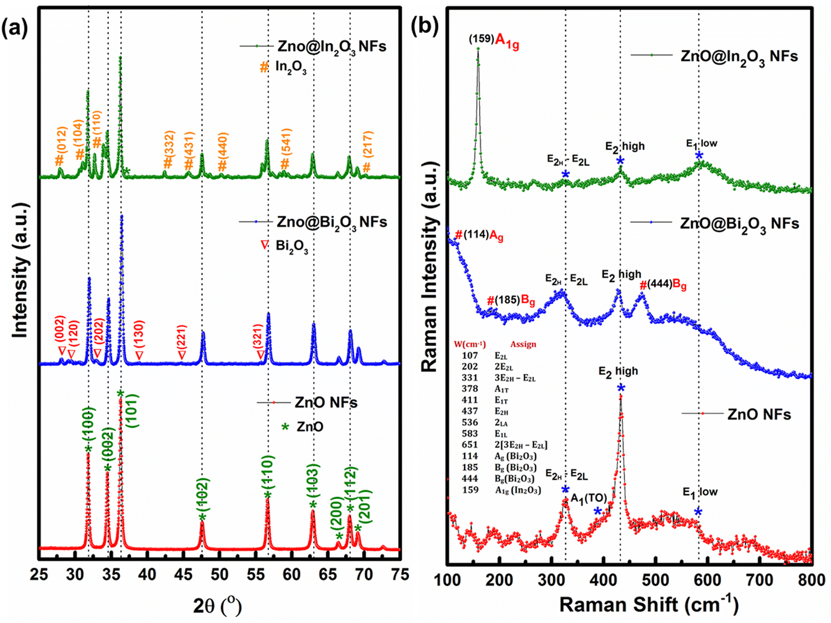 | ||
| Fig. 1 (a) XRD patterns and (b) Raman spectra of pristine ZnO, ZnO/Bi2O3 and ZnO/In2O3 HNFs. | ||
Fig. 1(b) depicts a comparison of Raman spectra acquired for pristine ZnO and n-ZnO/p-Bi2O3 and n-ZnO/n-In2O3 HNFs using the backscattering approach. Raman vibrational spectra of pure ZnO NFs were collected under ambient conditions which displayed a strong peak at 438 cm−1 corresponding to E2high vibration of ZnO that confirms the hexagonal wurtzite crystal phase. The strong peak of E2 mode confirmed the crystalline purity of ZnO NFs. The other two bands arise at the regions of lower wavenumber at 330 cm−1 and 378 cm−1 corresponding to the E2high–E2low and A1(TO) phonon vibrations modes. Similarly, the peaks observed at 330 cm−1 and 437 cm−1 can be ascribed to ZnO–zone boundary phonon vibrations.44 However, the peaks arising for ZnO in ZnO/Bi2O3 and ZnO/In2O3 HNFs were found to exhibit considerable peak shifts as described in Fig. 1(b), because of the accommodation of p-Bi2O3 and n-In2O3 NIs on ZnO surface. For n–p type ZnO/Bi2O3 HNFs, along with ZnO vibrations, the Raman shift observed at 114 cm−1 is revealed as Ag symmetry mode mainly due to the presence Bi atoms. The bands at 138 cm−1 (Ag), 185 cm−1, 444 cm−1 (Bg) might originate from the vibrations of both Bi3+ and O2− ions onto ZnO further confirming the effective formation of heterojunction with monoclinic α-Bi2O3 NIs. The E2(high) vibration peak in ZnO turns out to be quenched owing to the formation of p-Bi2O3 heterojunction with n-ZnO. Also, oxygen vacancies (Vo) and zinc interstitial (Znin) states can be confirmed from the disappearance of A1(LO) peak.45 Whereas, n–n type ZnO/In2O3 HNFs exhibited a highly intense peak at 159 cm−1 as presented in Fig. 1(b) revealing the presence of n-In2O3 NIs along with the significant n-ZnO bands. The intensity of all the peaks was quenched owing to the formation of n-In2O3 NIs onto the n-ZnO NFs. The vibration band associated with E1-LO vibrations of n-ZnO was reduced because of the interstitial defects, which represents a promising region for the growth of n-In2O3 NIs. Further, E2high vibrations were observed to be broad and weak, which confirms the heterojunction formation of In–O with Zn–O bonds.46 A wide hump revealed at 584 cm−1 ascribed to the E1-LO vibrations of n-ZnO confirms the existence of high-density oxygen vacancies (Vo) and zinc interstitials (Zni) in the materials. The formation of heterojunctions in the n–p and n–n type nanofibers promotes local electron transfer that can be revealed from the quenched vibrations of E2high and E1(LO) with substantial peak shifts found for both n-ZnO/p-Bi2O3 and n-ZnO/n-In2O3 HNFs that may enhance the NO2 sensing characteristics.
3.2. Morphological characterization of ZnO/Bi2O3 and ZnO/In2O3 HNFs
To gain more insights into the nanograined structure and heterojunctions of the ZnO/Bi2O3 and ZnO/In2O3 nanofibers, TEM analysis was performed. Fig. 2 depicts TEM and high-resolution TEM images and the corresponding selective area electron diffraction (SAED) patterns of n-ZnO/p-Bi2O3 and n-ZnO/n-In2O3 HNFs. Fig. 2(a and d) displays low-magnification images of ZnO/Bi2O3 and ZnO/In2O3 HNFs, confirming the nanograined morphology with high porosity, which can enhance the surface area and more active sites favouring the adsorption of target NO2 gas. The inset shows the TEM image of as-spun single nanofiber where the contrast clearly depicts the core–shell structure that can further limit the lattice doping during the annealing process which plays a crucial role in forming an effective heterojunction. From Fig. 2(a and d), the average grain sizes were estimated as 36 ± 6 nm for n-ZnO/p-Bi2O3 and 28 ± 4 for n-ZnO/n-In2O3 HNFs and having lengths of several micrometers with high aspect ratio, suitable for electronics and sensing applications. Fig. 2(b and e) presents the HRTEM images of n-ZnO/p-Bi2O3 and ZnO/In2O3 HNFs, which clearly revealed the existence of crystal plane fringes on each ZnO nanograin (NG) and Bi2O3 and In2O3 NIs. Further, to calculate the spacing between the planes of the crystals of n-ZnO/p-Bi2O3 and ZnO-In2O3, inverse FFT (IFFT) image processing was utilized as depicted in Fig. 2(b and e). Based on IFFT image analysis, the d-spacing value of ZnO NGs was calculated to be 2.48 Å, corresponding to the [101] plane, and 2.72 Å for Bi2O3 Nis, associated with the [121] lattice for n-ZnO/p-Bi2O3 HNFs.47 In the case of ZnO/In2O3 HNFs, the d-spacing of ZnO was estimated as 2.81 Å which revealed the [100] plane and d-spacing of 3.89 Å corresponding to In2O3 NIs that can be correlated to the [012] plane.48 The analogous SAED patterns of the HNFs clearly revealed the multi-crystalline nature of the materials with nanograined structure as shown in Fig. 2(c and e). Multi-crystalline, concentric diffraction rings appeared in SAED patterns illustrating ZnO (104), Bi2O3 (223), Bi2O3 (330), Bi2O3 (221), ZnO (100), Bi2O3 (031), ZnO (110), ZnO (200), ZnO (001) and ZnO (211) lattice planes (Fig. 2(c)) as referred to JCPDS card no. 36-1451 for wurtzite ZnO and correspondingly monoclinic α-Bi2O3 referred to JCPDS card no. 71-0465 for n-ZnO/p-Bi2O3 HNFs. Similarly, coaxial ring observed in the SAED pattern of n-ZnO/n-In2O3 HNFs depicted in Fig. 2(f) specifies the nature of polycrystallinity in the NGs corresponding to wurtzite ZnO and rhombohedral In2O3. The SAED pattern further revealed the features of ZnO (203), ZnO (104), ZnO (112), In2O3 (116), In2O3 (202), ZnO (101), In2O3 (012), ZnO (100), ZnO (002), In2O3 (024), In2O3 (300), ZnO (104) and In2O3 (128) lattice planes which were matched with standard for In2O3 (JCPDS card no. 73-1809).47,49 The HNFs exhibited nanograined morphology due to their intrinsic porosity and abundant surface area formed during the calcination process which could emboss n-ZnO/p-Bi2O3 and n-ZnO/n-In2O3 HNFs as efficient sensing materials with reduced operating temperature. The results indicated the existence of heterojunctions in the ZnO/Bi2O3 and ZnO/In2O3 HNFs at the interfaces. However, n-ZnO/p-Bi2O3 and ZnO/In2O3 HNFs showed typical nanograined structure with randomly oriented secondary p- and n-type MOS NIs. Possible alignment of the Fermi level with these secondary MOS nanograins occurs which could increase the overall electron density in both the HNF materials. Therefore, a corresponding increase in the rate of adsorption of NO2 through electronic sensitization could be possibly expected. | ||
| Fig. 2 (a) TEM images of n-ZnO/p-Bi2O3 HNFs (inset shows the as-spun core–shell nanofiber). (b) HRTEM image of n-ZnO/p-Bi2O3 HNFs and inverse FFT images of ZnO and Bi2O3 (inset shows the live FFT images of ZnO and Bi2O3). (c) SAED pattern of n-ZnO/p-Bi2O3 HNFs. (d) TEM images of n-ZnO/n-In2O3 HNFs (inset shows the as-spun core–shell nanofiber). (e) HRTEM image of n-ZnO/n-In2O3 NFs and inverse FFT images of ZnO and In2O3 (inset shows the live FFT images of ZnO and In2O3). (f) SAED pattern of n-ZnO/n-In2O3 HNFs. | ||
The porous structure of ZnO/Bi2O3 and ZnO/In2O3 HNFs was revealed from TEM analysis, which was further quantified using BET analysis. Detailed N2 adsorption–desorption analyses of pristine ZnO, n-ZnO/p-Bi2O3 and n-ZnO/n-In2O3 HNFs are shown in Fig. S3 (ESI†). BET surface area, pore volume and pore size for these HNFs were estimated from the BJH plots as summarized in Table S1 (ESI†). The specific surface area was estimated to be 16.012 m2 g−1 and 7.302 m2 g−1 and the corresponding pore volume was 3.52 cm3 g−1 and 2.84 cm3 g−1 for n-ZnO/p-Bi2O3 and n-ZnO/n-In2O3 HNFs, respectively. The enhanced surface area of HNFs results in abundant surface-active sites compared with bare ZnO NFs which provided facile electron transport and thereby enhanced the rate of NO2 adsorption.50
3.3. XPS analysis of ZnO/Bi2O3 and ZnO/In2O3 HNFs
In order to examine the interactions among n- and p-type MOS and n- and n-type MOS in the ZnO/Bi2O3 and ZnO/In2O3 HNFs and oxidation states of the elements, surface-sensitive X-ray photoelectron spectroscopic analysis was performed for pristine ZnO, n-ZnO/p-Bi2O3 and n-ZnO/n-In2O3 HNFs. Fig. 3(a) depicts the wide scan survey of pure ZnO, n-ZnO/p-Bi2O3 and n-ZnO/n-In2O3 HNFs, which revealed the presence of elemental peaks such as those of Zn, Bi, In and O which further confirms the absence of impurities in the HNFs. Fig. 3(b) displays the high-resolution Zn 2p XPS peaks corresponding to pristine ZnO, n-ZnO/p-Bi2O3 and n-ZnO/n-In2O3 HNFs. Fine scan of the Zn 2p peak reveals the incidence of two major peaks at binding energy of 1021.43 eV and 1044.68 eV attributed to Zn 2p3/2 and Zn 2p1/2 correspondingly, with an energy difference of 23.25 eV which indicated the bivalent oxidation state of ZnO NFs. Whereas, n-ZnO/p-Bi2O3 and n-ZnO/n-In2O3 HNFs revealed a minor shift to lower binding energy compared to pristine ZnO NFs owing to the surface lodging of Bi2O3 and In2O3 NIs and the presence of Zni defects in the NG morphology.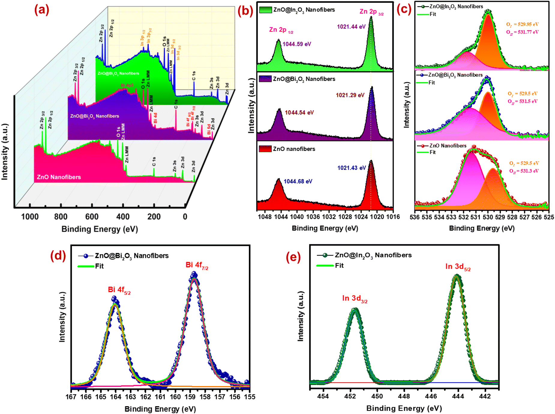 | ||
| Fig. 3 (a) XPS wide scan spectra of bare ZnO, n-ZnO/p-Bi2O3 and n-ZnO/n-In2O3 HNFs. Fine scan spectra of (b) Zn 2p, (c) O 1s and (d) Bi 4f peaks of n-ZnO/p-Bi2O3 and (e) In 3d peaks of n-ZnO/n-In2O3 HNFs. | ||
The high-resolution spectra of the O 1s band of n-ZnO/p-Bi2O3 and n-ZnO/n-In2O3 HNFs are shown in Fig. 3(c). The O 1s peaks in pure ZnO, n-ZnO/p-Bi2O3 and n-ZnO/n-In2O3 HNFs were deconvoluted into a couple of peaks indicating OI and OII; the one at 529.5 eV is attributed to lattice oxygen in Zn–O bonding and the other at 531.3 eV is associated with surface chemisorbed oxide species, either O− or O2− ions. It is noticed that the chemisorbed oxygen species is dominant in pure ZnO NFs as displayed in Fig. 3(c). However, OII peak was slightly suppressed in the cases of ZnO/In2O3 and ZnO/Bi2O3 nanofibers compared to OI peak owing to the formation of heterojunctions on ZnO nanofibers which could be correlated with the NO2 sensing properties.42 The intensity of OII peak was observed to be lower for n-ZnO/n-In2O3 than for n-ZnO/p-Bi2O3 HNFs due to fewer adsorbed surface oxide molecules. A corresponding shift in O 1s spectra also was observed at lower energy in contrast to bare ZnO NFs, which further confirmed the strong interaction at the ZnO/Bi2O3 and ZnO/In2O3 heterointerfaces. Also, the existence of more active sites and catalytic behavior of Bi2O3 and In2O3 NGs at the interface can indicate these materials as active sensing materials.
Moreover, Fig. 3(d and e) shows the high-resolution peaks of Bi 4f and In 3d peaks for n-ZnO/p-Bi2O3 and n-ZnO/n-In2O3 nanofibers, respectively. In the case of Bi2O3, the two peaks positioned at 158.7 and 163.8 eV are ascribed to Bi 4f7/2 and Bi 4f5/2 states as depicted in Fig. 3(d).51 While, Fig. 3(e) presents the fine scan spectrum of In 3d state of n-ZnO/n-In2O3 HNFs. For In2O3, the two peaks positioned at 442.8 and 450.4 eV are ascribed to In 3d5/2 and In 3d3/2 states, respectively.52 The analysis of surface oxidation states of p-type Bi2O3 and n-type In2O3 NIs grown on the surface of ZnO nanofibers further confirmed the existence of heterointerfaces which is essential for enhanced sensor performance.
3.4. Evaluation of NO2 sensing properties of aligned n–p type ZnO/Bi2O3 and n–n type ZnO/In2O3 HNFs
The aligned n-ZnO/p-Bi2O3 and n-ZnO/n-In2O3 HNFs were directly spun onto IDA transducer electrodes via the coaxial electrospinning method. Evaluation of NO2 sensing properties of these sensor devices was performed using an in-house gas sensor test station existing in our laboratory.40 Operating temperature of the HNFs has a vital role in enhancement in sensitivity and reliability of the sensor. The sensor response (S = [Rg − Ra]/Ra) was monitored while purging of 1 ppm NO2 gas with varying temperatures between 50 and 350 °C for pristine ZnO, n-ZnO/p-Bi2O3 and n-ZnO/n-In2O3 HNFs to determine the suitable operating temperature as shown in the insets of Fig. 4(a and c). It was found that the maximum sensitivity (S) toward 1 ppm of NO2 gas was achieved at 300 °C and 200 °C for aligned n-ZnO/p-Bi2O3 HNFs (324%) and aligned n-ZnO/n-In2O3 HNFs (415%), respectively. The exposure time was fixed as 30 s for all measurements. The optimum temperature for which the maximum response occurred was further chosen as the working temperatures of the sensors. The highest sensitivity for the pristine ZnO nanofibers was attained at 250 °C. The operating temperature was reduced for aligned n-ZnO/n-In2O3 HNFs compared with pristine ZnO, while that of aligned n-ZnO/p-Bi2O3 nanofibers remained the same, but with superior sensitivity. This study clearly revealed the impact of n–n type heterojunctions with improved electron carrier density that favored enhanced NO2 sensitivity. Even though the n-ZnO/p-Bi2O3 nanofibers possess superior sensitivity, holes are the majority carriers for p-type Bi2O3 semiconductor heterojunctions on ZnO nanofibers. The electron transfer among p-Bi2O3 and n-ZnO arises owing to the work function difference which further leads to the occurrence of electron depletion at the interface. Therefore, the activation energy essential to achieve high sensitivity is significantly high due to charge transfer to p-Bi2O3 nanoislands. However, the operating temperature of n-ZnO/p-Bi2O3 nanofibers was not found to be excessive compared to pristine ZnO. | ||
| Fig. 4 Dynamic sensor response and recovery profiles of (a) porous ZnO NFs, (b) n-ZnO/p-Bi2O3 HNFs and (c) n-ZnO/n-In2O3 HNFs. (Insets show sensor response towards 1 ppm of NO2 gas with varying temperature.) (d) Sensor response as a function of NO2 concentration. (e) log(Sgas − 1) versus log(Pgas) plot. (f) Changes in band bending (qΔV) with increase in NO2 concentration. | ||
The transient NO2 responses of pristine ZnO, n-ZnO/p-Bi2O3 and n-ZnO/n-In2O3 based aligned HNFs for a concentration of NO2 ranging from 500 ppb to 3 ppm are shown in Fig. 4(a–c). The variation in the resistance upon exposure to NO2 gas indicates the surface reaction with the chemisorbed oxygen on the nanograined surface. The difference in resistance was observed to be enlarged with an increase in NO2 concentration. The sensitivity ((Rg − Ra/Ra) × 100%) as a function of concentration of NO2 is depicted in Fig. 4(d). The results suggest a linear trend in the sensor response with increase in NO2 concentration. The NO2 gas sensing characteristics of the materials are tabulated in Table S2 (ESI†). The time required to attain 90% of variation in the overall resistance during/after exposure to NO2 was used to calculate the sensor response and recovery time. The NO2 sensing characteristics shown in Table S2 (ESI†) indicate that the sensitivity of pristine ZnO nanofibers is up to 31% for 500 ppb concentration of NO2 with response time of 9–10 s. Whereas, the n-ZnO/n-In2O3 HNFs shows enhanced sensitivity of ∼340% with rapid response (tres (90)) of 4–5 s compared to n-ZnO/p-Bi2O3 HNFs which exhibited a sensitivity of ∼365% with response time (tresp (90)) of 7–8 s. The boosted sensitivity observed for the HNFs was due to enhanced free carrier density at the heterojunction surface leading to fast charge transport while forming n–p and n–n heterojunctions. Prominently, the n-ZnO/n-In2O3 HNFs operated at reduced temperature with superior sensitivity owing to the charge transfer from n-In2O3 to n-ZnO owing to the work function variance. Therefore, charge accumulation could take place on ZnO, while charge depletion occurs at the In2O3 interfaces.
In order to investigate the chemisorbed oxygen species formed over the aligned ZnO/Bi2O3 and ZnO/In2O3 based HNFs, the slope of log(SGas − 1) versus log(PGas) was estimated as shown in Fig. 4(e). Moreover, from the relation (S = aCβ), the value of the exponent β could be used to understand the elementary reaction occurring on the material surface.53 From the slope in Fig. 4(e), the β values were estimated as 0.56 for aligned n-ZnO/n-In2O3 HNFs and 1.06 for aligned n-ZnO/p-Bi2O3 HNFs at the operational temperature signifying that the surface adsorbed oxygen ions majorly could be O− rather than O2− ions. It was established by previous reports that if β is near to ∼0.5, O2− ions could be adsorbed predominantly, and if β is ∼1, surface oxide ion species are mostly O−.54
Aligned HNFs have shown improved sensitivity due to the presence of more energetic O− ions which are chemically more active compared to O2− and could create additional favorable sites for surface catalytic processes. Upon exposure to NO2, the work function, electron affinity and surface band bending (qΔV) of the sensing materials tend to change. The surface band bending energies of both aligned ZnO/Bi2O3- and ZnO/In2O3-based HNFs were estimated based on their sensor responses. The band bending values (qΔV) were estimated for these HNFs based on their sensor response to varied NO2 concentrations.55,56 On analyzing qΔV of the HNFs, it was found that n-ZnO/n-In2O3 HNFs possessed higher energy than n-ZnO/p-Bi2O3 HNFs and pure n-ZnO NFs, because of a broad depletion region while purging NO2 as evident from Fig. 4(f).
Selectivity towards NO2 for n-ZnO/p-Bi2O3 and n-ZnO/n-In2O3 HNFs was further studied in the presence of possible interfering vapors such as NH3, H2S, SO2, C2H5OH and C3H6O. Both 1D aligned n-ZnO/p-Bi2O3 and n-ZnO/n-In2O3 HNFs revealed excellent selectivity towards NO2 at operating temperature due to the favored electron transport characteristics as a result of the existence of surface-anchored p-Bi2O3/n-In2O3 nanoclusters and intrinsic surface defect-mediated sensing properties as described in Fig. S4 (ESI†). Further, intervention of atmospheric moisture in the RH range of 10–95% on aligned n-ZnO/p-Bi2O3 and n-ZnO/n-In2O3 HNFs during NO2 sensing was examined as shown in Fig. S5(a and b) (ESI†). When the relative humidity was increased, the sensor response was found to be deteriorated for aligned n-ZnO/p-Bi2O3 HNFs owing to the interruption of hydroxide molecules which prevail on the HNF surface, reducing the flow of electrons. Whereas, aligned n-ZnO/n-In2O3 HNFs show a slight decrease in sensitivity as revealed from Fig. S5(b) (ESI†) and a relatively even response over the relative humidity range of 10–40%, owing to the higher charge carrier density along with abundant surface-active sites. When the humidity content increased above 40%, the interruption of moisture was found to be persistent on the HNFs which decreases the charge transport and thereby decreases the rate of adsorption of NO2 molecules. Furthermore, the response-recovery properties of aligned ZnO/Bi2O3 and ZnO/In2O3 HNFs were determined before and after 8 months for trace-level (1 ppm) NO2 under working conditions as shown in Fig. S6(a–d) (ESI†). Both 1D aligned n-ZnO/p-Bi2O3 and n-ZnO/n-In2O3 HNFs exhibited considerable stability even after 8 months during multiple cycles of NO2 exposure. Though a minimal 15% drop in the sensitivity was perceived, stable base resistance values were sustained under operational conditions, which proves the durability and repeatability of the HNF sensors.
3.5. In situ AC impedance studies of aligned n-ZnO/p-Bi2O3 and n-ZnO/n-In2O3 HNFs-based sensors
In order to explore the mechanism behind enhanced sensor performance associated with surface anchoring of p-Bi2O3 and n-In2O3 nanoclusters on nanograined n-ZnO nanofibers, in situ AC impedance spectroscopic studies were carried out in various atmospheric conditions such as room temperature condition, sensor operating temperature and while purging NO2. Impedance spectroscopic measurements were acquired using a solid-state two-electrode system. Scheme 2 shows a schematic representation of impedance analysis performed under various conditions. In situ Nyquist plots in the frequency range of 20 Hz to 10 MHz acquired for 1D aligned n-ZnO/p-Bi2O3 and n-ZnO/n-In2O3 are depicted in Fig. 5(a and b).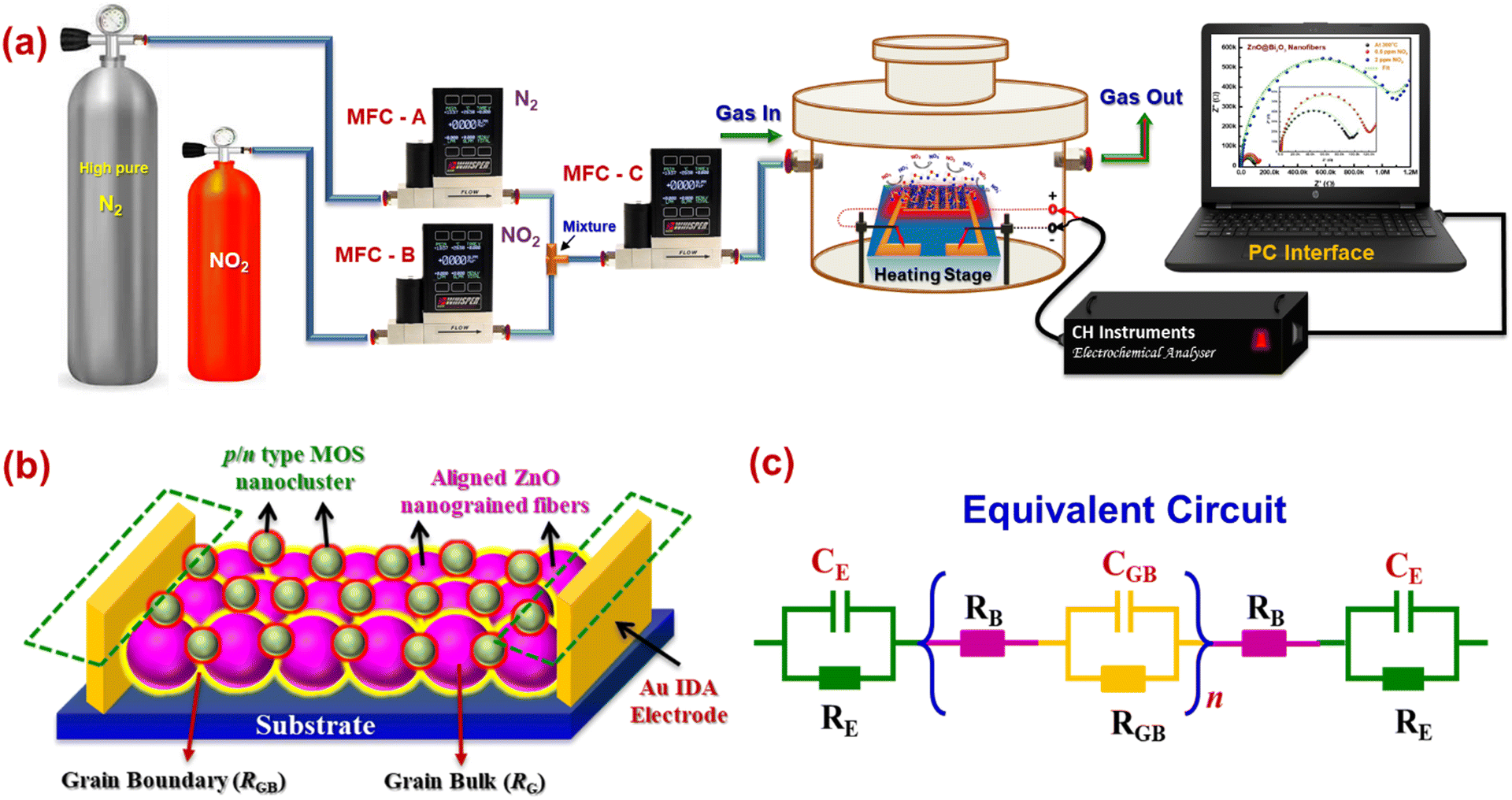 | ||
| Scheme 2 (a) Schematic illustration of the experimental setup used for AC impedance studies. (b) Porous layer of p/n MOS decorated ZnO nanofibers aligned between Au IDA electrodes. (c) Corresponding equivalent circuit. | ||
 | ||
| Fig. 5 In situ AC impedance measurements. Nyquist spectra of (a) ZnO/Bi2O3 and (b) ZnO/In2O3 HNFs at operating temperatures and during NO2 exposure. Insets show the corresponding equivalent circuits. | ||
Prior to the in situ studies, Nyquist plots for ZnO/Bi2O3 and ZnO/In2O3 were acquired under ambient conditions and operating temperature to explore the charge transport phenomenon. At room temperature, both ZnO/Bi2O3 and ZnO/In2O3 HNFs possessed minimal conductivity as evident from the distorted I–S spectra as shown in Fig. S7(a and b) (ESI†). Whereas, as the conductivity of the sensor increased, the imaginary component (Z′′) versus the real component (Z′) in the impedance spectra exhibited a perfect semicircle trend from low-frequency to high-frequency region, upon elevating the temperature up to operating temperature confirming the typical semiconductor behaviour.57 Moreover, the characteristic semicircle arc followed by the Nyquist spectra confirms the grain–grain boundary induced conduction mechanism and the diameter of the semicircle was increased with respect to NO2 concentration. The high-frequency region in the impedance spectra represents the material's grain-bulk (ZG) characteristics, median-frequency region signifies the grain boundary (ZGB) characteristics and lower-frequency region indicates the electrode to material contact characteristics.38 The corresponding electrical equivalent circuit model was used to understand the major contribution either by nanograins or by grain boundaries, or the heterojunctions in the nanofibers.
The circuit model is expressed as a set of resistor–capacitor (RC) series circuit components as indicated in the insets of Fig. 5(a and b). The net impedance (ZI) of ZnO/Bi2O3 and ZnO/In2O3 HNFs is expressed as38
| ZI = Z0 + ZG + ZGB | (1) |
Nyquist plots for n-ZnO/p-Bi2O3 and n-ZnO/n-In2O3 HNFs were acquired under different temperatures and are depicted in Fig. S7(a and b) (ESI†). A reduced trend in the semicircle plot was observed which indicated that the resistance decreases as a function of temperature. This behaviour confirmed the negative temperature coefficient of resistance (NTCR) owing to the semiconductor nature of the sensor materials used for this investigation. The results suggest that electrical conduction could be larger at high temperatures. In order to calculate the activation energy (Ea), the following relation was used:53
| R = R0 exp(−Ea/kBT) | (2) |
The conduction mechanism of ZnO/Bi2O3 and ZnO/In2O3 HNFs-based sensors was further investigated during exposure to NO2. The impedance measurements were performed by purging of 100 sccm of 0.5–2 ppm concentration range of NO2. The acquired Nyquist spectra clearly show a decrease in the conductivity when the sensor was exposed to NO2. From the corresponding equivalent circuit, the resistances of grain and grain boundaries were estimated, which revealed the complex sensing phenomenon behind significant changes occurring upon NO2 adsorption. Fig. 5(a and b) presents the Nyquist plots corresponding to n-ZnO/p-Bi2O3 and n-ZnO/n-In2O3 HNFs under air and NO2 atmospheres. Nyquist spectra of both sensors under ambient environment showed negligible conductivity owing to the large Schottky barrier existing at the inter-grain interfaces. At working temperature in air condition of both n-ZnO/p-Bi2O3 and n-ZnO/n-In2O3 HNFs, grain bulk (ZG) and grain boundary (ZGB) resistances of HNFs have equal contributions towards charge transfer owing to the higher electron mobility. When exposed to 0.5 ppm NO2, the major contribution was found to be from nanofiber grain boundary rather than the contribution from the grain bulk for n-ZnO/p-Bi2O3 and n-ZnO/n-In2O3 HNFs as quantified in Table S3 (ESI†). It is evident that only the barrier potential of grain boundaries gets altered while grain bulk remains unchanged upon exposure to lower concentration since the NO2 molecules trap free electrons from the surface of nanograins. Moreover, large change in the grain bulk and grain-boundary resistances was observed for n-ZnO/p-Bi2O3 and n-ZnO/n-In2O3 HNFs for 2 ppm of NO2, which may be the cause of the superior sensitivity compared to bare ZnO.
The barrier potential of grain bulk and grain boundary increases for both n-ZnO/p-Bi2O3 and n-ZnO/n-In2O3 HNFs owing to the strong interaction of NO2 with the surface adsorbates (O− ions) and thereby pulling more electrons from the grain bulk (ZG). The results suggest that at the sensor operating temperature, more free electrons originate due to the charge transfer process occurring at the n–p and n–n interfaces of HNFs. When the sensors were exposed to trace-level concentration of NO2, these free electrons were trapped via surface adsorbed molecular oxygen (O−) and thereby captured more electrons from the interfacial grain boundaries of the HNFs. Upon exposure to higher concentration of NO2, along with grain boundaries (ZGB), NO2 could abstract additional electrons from the grain bulk (ZGB) thereby increasing the sensor resistance rapidly which increased the potential barrier height. This result further confirmed that the grain boundary (ZGB) of ZnO/Bi2O3 and ZnO/In2O3 HNFs is largely affected by NO2 molecules which remained as the major reason behind the superior conduction in the HNFs.
The transport characteristics such as charge carrier density and width of the depletion layer were further estimated from the in situ impedance spectroscopic analysis under different conditions. Based on the Poisson equation, the relation between the barrier potential height and capacitance can be derived from the depletion approximation given as
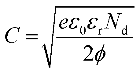 | (3) |
 | (4) |
 | (5) |
After introducing NO2, the carrier density (Nd) was found to be reduced drastically from 1.63 × 10¹⁹ to 0.98 × 1019 cm−2 for n-ZnO/p-Bi2O3 and from 1.44 × 10¹⁹ to 0.53 × 1019 cm−2 for n-ZnO/n-In2O3 HNFs.58,59
Accordingly, the depletion takes place on the surface of the HNFs due to reduction in the electron concentration as estimated by I–S studies for n-ZnO/p-Bi2O3 and n-ZnO/n-In2O3 HNFs using eqn (5). The depletion layer width (W) was observed to be enlarged from 2.16 nm to 2.76 nm for n-ZnO/p-Bi2O3 and from 2.12 nm to 3.48 nm for n-ZnO/n-In2O3 HNFs when NO2 was purged at the working temperature and the results are summarized in Table S4 (ESI†). The reduction in charge carrier density is due to the charge recombination process during surface adsorption of NO2 molecules on the HNFs which attract more electrons from the grain bulk and grain boundaries. Considering the aforementioned experimental results, it might therefore be confirmed that the difference in the rate of charge carrier density of n-ZnO/n-In2O3 HNFs was found to be higher compared to n-ZnO/p-Bi2O3 when exposed to NO2. However, from the AC impedance spectra, it was ascertained that the large variation of charge transport characteristics upon exposure to NO2 is owing to the large accumulation of free charge carriers at the interface of n–n type ZnO/In2O3 compared to that of n–p type heterojunction materials. Whereas, the built-in potential appearing while forming n–p type heterojunction slightly hinders the free charge carriers on the surface of the material owing to the presence of a hole accumulation regime. Under operational conditions, a large quantity of holes is accumulated by p-Bi2O3 nanoclusters on the surface which leads to narrowing of the conduction channel of n-ZnO, and further thermal activation was required for greater response towards NO2. As observed from the AC impedance studies, the resistance of grain bulk and grain boundary nanojunction increases during NO2 exposure for both n–p and n–n type HNF materials which can be further explored along with great variation in the conduction mechanism among the two different combinations.
Typically, when the HNF-based sensors are exposed to air environment in operational conditions, adsorption of oxide ions on the HNF surface occurs which further traps freely available electrons leading to the formation of an electron depletion region over the HNF surface. Moreover, from β values derived from the response graph, the adsorbed oxygen species on aligned ZnO/Bi2O3 and ZnO/In2O3 HNFs were found to be O− rather than O2− ions. In order to understand the energy levels of ZnO/Bi2O3 and ZnO/In2O3 HNFs, a hypothetical band structure was constructed by AFORS-HET v2.5, as represented in Scheme 3. Energy level bending characteristics of ZnO/Bi2O3 and ZnO/In2O3 HNFs before and after NO2 exposure were discussed in our previous report.54,60 When n- and p-type MOSs are electrically connected to form n–p heterojunctions, orientation of Fermi levels (Ef) takes place as a result of work function difference; i.e., electrons can move from higher occupied states to lower unoccupied states between the n-ZnO and p-Bi2O3 heterojunctions further to align the Ef and thereby enhance the electron density.25,61 Therefore, transferred electrons accumulate at the interface of the lower Fermi energy level and depletion takes place at the higher Fermi energy level junction which could continue until a stable equilibrium state is achieved. Whereas, feasible charge transport occurs near the interface of n–n junction (n-ZnO/n-In2O3) because of the minimal variances in the conduction band states. Consequently, an easy formation of electron accumulation at one junction is more dominant than forming a depletion region at the other interface. Hence, the conduction band with higher energy state (n-In2O3) exhibits a loss of electrons, whereas the conduction band with comparatively lower energy state (n-ZnO) receives more transferred electrons and forms an electron accumulation region. This results in subsequent ionosorption (O−) near the electron accumulation region and thereby widens the barrier potential and effectively increases the sensitivity towards NO2 gas.62 Hence, n-ZnO/n-In2O3 HNFs exhibited enhanced sensitivity under reduced operating temperature.
 | ||
| Scheme 3 (a, b, e and f) Simulated energy band diagram before and after contact. (c and d) Schematic representation of mechanism of band bending in n-ZnO/p-Bi2O3 HNFs before and after NO2 exposure. (g and h) Schematic representation of band bending mechanism in n-ZnO/n-In2O3 HNFs before and after NO2 exposure. | ||
Although the sensing mechanism was deduced in terms of energy band structure, the nature of sensing materials also plays a vital role in enhancing the rate of NO2 adsorption. Though a 1D nanostructure offers better performance compared to other morphologies, the additional benefits from nanograined assisted 1D morphology leads to abundant active sites with high surface area and high aspect ratio. From the in situ impedance spectroscopic measurements, the conduction mechanism has been explored with the help of fitted equivalent circuits, which revealed the role of grains and grain boundary interactions in enhancing the NO2 sensitivity. Hence, it is confirmed that the superior sensitivity is owing to the existence of ZnO/Bi2O3 and ZnO/In2O3 heterojunctions. The presence of ZnO nanograins with p-Bi2O3 and n-In2O3 formed in the multi-crystalline nanofibers induced abundant grain boundaries between these nanograins, which also act as a potential barrier for further electron transfer. Upon exposure to NO2, the depletion region becomes wider and narrows the conduction channel due to expansion of depletion width. Therefore, the direct electron transport properties of multi-crystalline nanofibers make them promising as a better sensor material compared to crystalline nanorods. The results suggest that single-step production of MOS-based 1D aligned multi-crystalline HNFs could be a low-cost direct fabrication method for the development of superior real-time gas sensor devices with improved selectivity and likewise to bridge the gaps between the pilot-scale research and industrial manufacturing to make better products.
5. Conclusions
To summarize, aligned n-ZnO/p-Bi2O3 and n-ZnO/n-In2O3 HNFs produced using single-step on-chip fabrication have been demonstrated as active materials for NO2 sensor application, the method using coaxial electrospinning which does not involve any tedious and time-consuming steps due to elimination of wet-chemical processes. Characterization of the materials affirmed the existence of heterojunctions in n-ZnO/p-Bi2O3 and n-ZnO/n-In2O3 HNFs and illustrated the presence of catalytic MOS nanoislands anchored uniformly on the surface of ZnO nanofibers. The operating temperature was increased for n-ZnO/p-Bi2O3 (300 °C) and decreased for n-ZnO/n-In2O3 HNFs (200 °C) compared to pristine ZnO NFs (250 °C). The improved sensitivity and selectivity of aligned n-ZnO/p-Bi2O3 and n-ZnO/n-In2O3 HNFs are attributed to the successful formation of n–p and n–n heterojunctions and more active sites, which resulted in fast response (5–7 s) and ten-fold higher response than ZnO nanofibers for trace-level concentration of NO2 (500 ppb). It was confirmed that the enhanced NO2 sensing properties are owing to the nature of nanograined NF structure along with sufficient active sites on the catalytic MOS nanoclusters, increasing the carrier density thereby trapping further O− ions on the HNF surface while creating more electron donors with higher barrier potential at the interfaces. The conduction mechanism based on electronic sensitization occurring in the HNFs was investigated using in situ AC impedance spectroscopic studies, which confirmed the role of modulation of grain bulk and grain boundary resistance and charge transfer between n–p and n–n type heterojunction materials. During in situ NO2 exposure, the carrier density (Nd) was found to be reduced drastically from 1.63 × 10¹⁹ to 0.98 × 1019 cm-2 for n-ZnO/p-Bi2O3 and from 1.44 × 10¹⁹ to 0.53 × 1019 cm-2 for n-ZnO/n-In2O3 HNFs. Accordingly, the depletion layer width (W) was estimated which was found to be increased from 2.16 nm to 2.76 nm for n-ZnO/p-Bi2O3 and from 2.12 nm to 3.48 nm for n-ZnO/n-In2O3 HNFs. This investigation unveiled the complex sensing phenomenon related to electron transfer via grain–grain boundary interactions existing while forming a heterojunction with ZnO, which is the underlying major reason behind the enhancement of NO2 sensing properties. Hence, 1D aligned MOS-based HNFs fabricated by a single-step process are promising for developing cost-effective NO2 sensors with excellent sensitivity.Author contributions
Ramakrishnan Vishnuraj: methodology, conceptualization, NO2 sensor analysis, in situ impedance spectroscopic analysis, data analysis, manuscript preparation. Mahaboobbatcha Aleem: energy band diagram simulation and analysis. Keerthi G Nair: XPS spectra fitting and analysis. Biji Pullithadathil: conceptualization, methodology, data analysis, manuscript preparation, supervision, resources and funding.Conflicts of interest
There are no conflicts to declare.Acknowledgements
The authors acknowledge Department of Science and Technology, Ministry of Science and Technology, India (ref. no. DST/TMD/HFC/2K18/55(C)) for financial support. The authors also wish to acknowledge the facilities and support provided by the management, PSG Sons and Charities, Coimbatore. The authors thank Dr Anuradha Ashok and Mr Vijayaraghavan, PSG IAS, Coimbatore for TEM measurements.References
- W. de Vries, Impacts of nitrogen emissions on ecosystems and human health: A mini review, Curr. Opin. Environ. Sci. Health, 2021, 21, 100249 CrossRef.
- K. Sur, V. K. Verma and B. Pateriya, Variation of tropospheric NO2 over Indo-Gangetic plain during COVID-19 outbreak in India, Spat. Inf. Res., 2021, 29, 841–855 CrossRef.
- H. Khan, A. Zavabeti, Y. Wang, C. J. Harrison, B. J. Carey, M. Mohiuddin, A. F. Chrimes, I. A. De Castro, B. Y. Zhang, Y. M. Sabri, S. K. Bhargava, J. Z. Ou, T. Daeneke, S. P. Russo, Y. Li and K. Kalantar-Zadeh, Quasi physisorptive two dimensional tungsten oxide nanosheets with extraordinary sensitivity and selectivity to NO2, Nanoscale, 2017, 9, 19162–19175 RSC.
- W. Qin, Z. Yuan, H. Gao, R. Zhang and F. Meng, Perovskite-structured LaCoO3 modified ZnO gas sensor and investigation on its gas sensing mechanism by first principle, Sens. Actuators, B, 2021, 341, 130015 CrossRef CAS.
- H. Zhu, Z. Yuan, Y. Shen, C. Han, H. Ji, Z. Mu and F. Meng, Conductometric acetic anhydride gas sensors based on S-doped porous ZnO microspheres with enhanced Lewis base interaction, Sens. Actuators, B, 2022, 373, 132726 CrossRef CAS.
- F. Meng, X. Shi, Z. Yuan, H. Ji, W. Qin, Y. B. Shen and C. Xing, Detection of four alcohol homologue gases by ZnO gas sensor in dynamic interval temperature modulation mode, Sens. Actuators, B, 2022, 350, 130867 CrossRef CAS.
- Y. Kang, F. Yu, L. Zhang, W. Wang, L. Chen and Y. Li, Review of ZnO-based nanomaterials in gas sensors, Solid State Ionics, 2021, 360, 115544 CrossRef CAS.
- J. Wang, M. Yu, X. Li and Y. Xia, UV-enhanced NO 2 gas sensing properties of polystyrene sulfonate functionalized ZnO nanowires at room temperature, Inorg. Chem. Front., 2019, 6, 176–183 RSC.
- A. Sharma, M. Tomar and V. Gupta, A low temperature operated NO2 gas sensor based on TeO 2/SnO2 p-n heterointerface, Sens. Actuators, B, 2013, 176, 875–883 CrossRef CAS.
- S. W. Choi, A. Katoch, J. H. Kim and S. S. Kim, Prominent reducing gas-sensing performances of n-SnO2 nanowires by local creation of p-n heterojunctions by functionalization with p-Cr2O3 nanoparticles, ACS Appl. Mater. Interfaces, 2014, 6, 17723–17729 CrossRef CAS PubMed.
- W. Maziarz, TiO2/SnO2 and TiO2/CuO thin film nano-heterostructures as gas sensors, Appl. Surf. Sci., 2019, 480, 361–370 CrossRef CAS.
- D. R. Miller, S. A. Akbar and P. A. Morris, Nanoscale metal oxide-based heterojunctions for gas sensing: A review, Sens. Actuators, B, 2014, 204, 250–272 CrossRef CAS.
- M. Nakamura, A. Sawa, J. Fujioka, M. Kawasaki and Y. Tokura, Interface band profiles of Mott-insulator/Nb: SrTiO3 heterojunctions as investigated by optical spectroscopy, Phys. Rev. B: Condens. Matter Mater. Phys., 2010, 82, 4–7 Search PubMed.
- F. Li, X. Gao, R. Wang, T. Zhang, G. Lu and N. Barsan, Design of Core-Shell Heterostructure Nanofibers with Different Work Function and Their Sensing Properties to Trimethylamine, ACS Appl. Mater. Interfaces, 2016, 8, 19799–19806 CrossRef CAS PubMed.
- Q. Sun, J. Wang, J. Hao, S. Zheng, P. Wan, T. Wang, H. Fang and Y. Wang, SnS2/SnS p-n heterojunctions with an accumulation layer for ultrasensitive room-temperature NO2 detection, Nanoscale, 2019, 11, 13741–13749 RSC.
- X. Zhang, Y. Liu, H. Liu, T. Liang, P. Zhang and Z. Dai, FeSe2/Hematite n-n heterojunction with oxygen spillover for highly efficient NO2 gas sensing, Sens. Actuators, B, 2021, 345, 130357 CrossRef CAS.
- N. Kaur, M. Singh and E. Comini, One-Dimensional Nanostructured Oxide Chemoresistive Sensors, Langmuir, 2020, 36, 6326–6344 CrossRef CAS PubMed.
- S. Bai, H. Fu, Y. Zhao, K. Tian, R. Luo, D. Li and A. Chen, On the construction of hollow nanofibers of ZnO-SnO2 heterojunctions to enhance the NO2 sensing properties, Sens. Actuators, B, 2018, 266, 692–702 CrossRef CAS.
- H. Shin, W. G. Jung, D. H. Kim, J. S. Jang, Y. H. Kim, W. T. Koo, J. Bae, C. Park, S. H. Cho, B. J. Kim and I. D. Kim, Single-Atom Pt Stabilized on One-Dimensional Nanostructure Support via Carbon Nitride/SnO2Heterojunction Trapping, ACS Nano, 2020, 14, 11394–11405 CrossRef CAS PubMed.
- W. Avansi, A. C. Catto, L. F. Da Silva, T. Fiorido, S. Bernardini, V. R. Mastelaro, K. Aguir and R. Arenal, One-Dimensional V2O5/TiO2 Heterostructures for Chemiresistive Ozone Sensors, ACS Appl. Nano Mater., 2019, 2, 4756–4764 CrossRef CAS.
- S. Ng, J. Prášek, R. Zazpe, Z. Pytlíček, Z. Spotz, J. R. Pereira, J. Michalička, J. Přikryl, M. Krbal, H. Sopha, J. Hubálek and J. M. MacÁk, Atomic Layer Deposition of SnO2-Coated Anodic One-Dimensional TiO2Nanotube Layers for Low Concentration NO2Sensing, ACS Appl. Mater. Interfaces, 2020, 12, 33386–33396 CrossRef CAS PubMed.
- V. Ramakrishnan, R. Unnathpadi and B. Pullithadathil, p-Co3O4 supported heterojunction Carbon Nanofibers for Ammonia gas sensor applications, J. Mater. Nanosci., 2022, 9, 61–67 Search PubMed.
- T. Zhou and T. Zhang, Recent Progress of Nanostructured Sensing Materials from 0D to 3D: Overview of Structure–Property-Application Relationship for Gas Sensors, Small Methods, 2021, 5, 1–32 Search PubMed.
- J. H. Kim, A. Katoch, S. H. Kim and S. S. Kim, Chemiresistive Sensing Behavior of SnO2 (n)-Cu2O (p) Core-Shell Nanowires, ACS Appl. Mater. Interfaces, 2015, 7, 15351–15358 CrossRef CAS PubMed.
- G. J. Sun, J. K. Lee, S. Choi, W. I. Lee, H. W. Kim and C. Lee, Selective Oxidizing Gas Sensing and Dominant Sensing Mechanism of n-CaO-Decorated n-ZnO Nanorod Sensors, ACS Appl. Mater. Interfaces, 2017, 9, 9975–9985 CrossRef CAS PubMed.
- N. A. Isaac, I. Pikaar and G. Biskos, Metal oxide semiconducting nanomaterials for air quality gas sensors: operating principles, performance, and synthesis techniques, Microchim. Acta, 2022, 189, 196, DOI:10.1007/s00604-022-05254-0.
- M. Mousavi, M. B. Ghasemian, J. Han, Y. Wang, R. Abbasi, J. Yang, J. Tang, S. A. Idrus-Saidi, X. Guan, M. J. Christoe, S. Merhebi, C. Zhang, J. Tang, R. Jalili, T. Daeneke, T. Wu, K. Kalantar-Zadeh and M. Mayyas, Bismuth telluride topological insulator synthesized using liquid metal alloys: Test of NO2 selective sensing, Appl. Mater. Today, 2021, 22, 100954 CrossRef.
- A. K. Elger and C. Hess, Application of Raman spectroscopy to working gas sensors: From in situ to operando studies, Sensors, 2019, 19(23), 5075 CrossRef PubMed.
- N. Sergent, M. Epifani, E. Comini, G. Faglia and T. Pagnier, Interactions of nanocrystalline tin oxide powder with NO2: A Raman spectroscopic study, Sens. Actuators, B, 2007, 126, 1–5 CrossRef CAS.
- J. Zhang, D. Zeng, Q. Zhu, J. Wu, Q. Huang and C. Xie, Effect of Nickel Vacancies on the Room-Temperature NO2 Sensing Properties of Mesoporous NiO Nanosheets, J. Phys. Chem. C, 2016, 120, 3936–3945 CrossRef CAS.
- P. Hozák, M. Vorokhta, I. Khalakhan, K. Jarkovská, J. Cibulková, P. Fitl, J. Vlček, J. Fara, D. Tomeček, M. Novotný, M. Vorokhta, J. Lančok, I. Matolínová and M. Vrňata, New Insight into the Gas-Sensing Properties of CuOx Nanowires by Near-Ambient Pressure XPS, J. Phys. Chem. C, 2019, 123, 29739–29749 CrossRef.
- X. Xiao, L. Liu, J. Ma, Y. Ren, X. Cheng, Y. Zhu, D. Zhao, A. A. Elzatahry, A. Alghamdi and Y. Deng, Ordered Mesoporous Tin Oxide Semiconductors with Large Pores and Crystallized Walls for High-Performance Gas Sensing, ACS Appl. Mater. Interfaces, 2018, 10, 1871–1880 CrossRef CAS PubMed.
- D. Degler, N. Barz, U. Dettinger, H. Peisert, T. Chassé, U. Weimar and N. Barsan, Extending the toolbox for gas sensor research: Operando UV/vis diffuse reflectance spectroscopy on SnO2-based gas sensors, Sens. Actuators, B, 2016, 224, 256–259 CrossRef CAS.
- C. Drouilly, J. M. Krafft, F. Averseng, S. Casale, D. Bazer-Bachi, C. Chizallet, V. Lecocq, H. Vezin, H. Lauron-Pernot and G. Costentin, ZnO oxygen vacancies formation and filling followed by in situ photoluminescence and in situ EPR, J. Phys. Chem. C, 2012, 116, 21297–21307 CrossRef CAS.
- S. C. Navale, V. Ravi, D. Srinivas, I. S. Mulla, S. W. Gosavi and S. K. Kulkarni, EPR and DRS evidence for NO2 sensing in Al-doped ZnO, Sens. Actuators, B, 2008, 130, 668–673 CrossRef CAS.
- F. Schipani, D. R. Miller, M. A. Ponce, C. M. Aldao, S. A. Akbar and P. A. Morris, Electrical Characterization of Semiconductor Oxide-Based Gas Sensors Using Impedance Spectroscopy: A Review, Rev. Adv. Sci. Eng., 2016, 5, 86–105 CrossRef.
- H. S. Magar, R. Y. A. Hassan and A. Mulchandani, Electrochemical impedance spectroscopy (Eis): Principles, construction, and biosensing applications, Sensors, 2021, 21(19), 6578, DOI:10.3390/s21196578.
- V. Balasubramani, S. Sureshkumar, T. S. Rao and T. M. Sridhar, Impedance Spectroscopy-Based Reduced Graphene Oxide-Incorporated ZnO Composite Sensor for H2S Investigations, ACS Omega, 2019, 4, 9976–9982 CrossRef CAS PubMed.
- Y. Wang, A. Maity, X. Sui, H. Pu, S. Mao, N. K. Singh and J. Chen, In Operando Impedance Spectroscopic Analysis on NiO-WO3 Nanorod Heterojunction Random Networks for Room-Temperature H2S Detection, ACS Omega, 2018, 3, 18685–18693 CrossRef CAS PubMed.
- R. Vishnuraj, J. Dhakshinamoorthy, K. G. Nair, M. Aleem and B. Pullithadathil, MEMS-compatible, gold nanoisland anchored 1D aligned ZnO heterojunction nanofibers: Unveiling the NO2sensing mechanism with: Operando photoluminescence studies, Mater. Adv., 2021, 2, 3000–3013 RSC.
- D. V. Ponnuvelu, S. Abdulla and B. Pullithadathil, Novel Electro-Spun Nanograined ZnO/Au Heterojunction Nanofibers and Their Ultrasensitive NO2 Gas Sensing Properties, ChemistrySelect, 2018, 3, 7156–7163 CrossRef CAS.
- S. Balachandran and M. Swaminathan, Facile fabrication of heterostructured Bi2O3-ZnO photocatalyst and its enhanced photocatalytic activity, J. Phys. Chem. C, 2012, 116, 26306–26312 CrossRef CAS.
- F. Liu, G. Huang, X. Wang, X. Xie, G. Xu, G. Lu, X. He, J. Tian and H. Cui, High response and selectivity of single crystalline ZnO nanorods modified by In2O3 nanoparticles for n-butanol gas sensing, Sens. Actuators, B, 2018, 277, 144–151 CrossRef CAS.
- R. Zhang, P. G. Yin, N. Wang and L. Guo, Photoluminescence and Raman scattering of ZnO nanorods, Solid State Sci., 2009, 11, 865–869 CrossRef CAS.
- B. Karthikeyan, R. Udayabhaskar and A. Kishore, Appl. Phys. A: Mater. Sci. Process., 2014, 117, 1409–1414 CrossRef CAS.
- S. Sahoo, A. P. S. Gaur, A. K. Arora and R. S. Katiyar, Optical properties of In2O3 octahedra nano-beads grown on ZnO nanowires, Chem. Phys. Lett., 2011, 510, 242–245 CrossRef CAS.
- Z. Xue, Z. Cheng, J. Xu, Q. Xiang, X. Wang and J. Xu, Controllable Evolution of Dual Defect Zni and VO Associate-Rich ZnO Nanodishes with (0001) Exposed Facet and Its Multiple Sensitization Effect for Ethanol Detection, ACS Appl. Mater. Interfaces, 2017, 9, 41559–41567 CrossRef CAS PubMed.
- Y. V. Kaneti, Z. Zhang, J. Yue, Q. M. D. Zakaria, C. Chen, X. Jiang and A. Yu, Crystal plane-dependent gas-sensing properties of zinc oxide nanostructures: Experimental and theoretical studies, Phys. Chem. Chem. Phys., 2014, 16, 11471–11480 RSC.
- S. Bai, L. Quan, P. Tang, Y. Zhao, R. Luo, A. Chen, D. Li and N. Han, Controllable Synthesis and Gas-Sensing Properties of Zinc Oxide Nanocrystals with Exposed Different Percentage of Facets, IEEE Sens. J., 2016, 16, 866–872 CAS.
- K. Zhang, S. Qin, P. Tang, Y. Feng and D. Li, Ultra-sensitive ethanol gas sensors based on nanosheet-assembled hierarchical ZnO-In2O3 heterostructures, J. Hazard. Mater., 2020, 391, 122191 CrossRef CAS PubMed.
- J. Xu and J. Liu, Facet-selective epitaxial growth of δ-Bi2O3 on ZnO nanowires, Chem. Mater., 2016, 28, 8141–8148 CrossRef CAS.
- H. Liu, H. Zhai, C. Hu, J. Yang and Z. Liu, Hydrothermal synthesis of In2O3 nanoparticles hybrid twins hexagonal disk ZnO heterostructures for enhanced photocatalytic activities and stability, Nanoscale Res. Lett., 2017, 12, 2–11 CrossRef PubMed.
- J. Dhakshinamoorthy and B. Pullithadathil, New Insights Towards Electron Transport Mechanism of Highly Efficient p-Type CuO (111) Nanocuboids-Based H2S Gas Sensor, J. Phys. Chem. C, 2016, 120, 4087–4096 CrossRef CAS.
- V. Ramakrishnan, K. G. Nair, J. Dhakshinamoorthy, K. R. Ravi and B. Pullithadathil, Porous, n-p type ultra-long, ZnO@Bi2O3 heterojunction nanorods - Based NO2 gas sensor: New insights towards charge transport characteristics, Phys. Chem. Chem. Phys., 2020, 22, 7524–7536 RSC.
- M. E. Mazhar, G. Faglia, E. Comini, D. Zappa, C. Baratto and G. Sberveglieri, Kelvin probe as an effective tool to develop sensitive p-type CuO gas sensors, Sens. Actuators, B, 2016, 222, 1257–1263 CrossRef CAS.
- M. Hübner, C. E. Simion, A. Tomescu-Stanoiu, S. Pokhrel, N. Bârsan and U. Weimar, Influence of humidity on CO sensing with p-type CuO thick film gas sensors, Sens. Actuators, B, 2011, 153, 347–353 CrossRef.
- A. Labidi, C. Jacolin, M. Bendahan, A. Abdelghani, J. Guérin, K. Aguir and M. Maaref, Impedance spectroscopy on WO3 gas sensor, Sens. Actuators, B, 2005, 106, 713–718 CrossRef CAS.
- K. Guruprasad, G. Marappan, S. Elangovan, S. Velappa Jayaraman, K. Kamala Bharathi, G. Venugopal, C. Di Natale and Y. Sivalingam, Electrical transport properties and impedance analysis of Au/ZnO nanorods/ITO heterojunction device, Nano Express, 2020, 1, 030020, DOI:10.1088/2632-959X/abc6f8.
- F. Schipani, D. R. Miller, M. A. Ponce, C. M. Aldao, S. A. Akbar, P. A. Morris and J. C. Xu, Conduction mechanisms in SnO2 single-nanowire gas sensors: An impedance spectroscopy study, Sens. Actuators, B, 2017, 241, 99–108 CrossRef CAS.
- R. Vishnuraj, K. K. Karuppanan, M. Aleem and B. Pullithadathil, Boosting the performance of NO2gas sensors based on n-n type mesoporous ZnO@In2O3heterojunction nanowires:in situconducting probe atomic force microscopic elucidation of room temperature local electron transport, Nanoscale Adv., 2020, 2, 4785–4797 RSC.
- D. Zhang, Y. Cao, J. Wu and X. Zhang, Tungsten trioxide nanoparticles decorated tungsten disulfide nanoheterojunction for highly sensitive ethanol gas sensing application, Appl. Surf. Sci., 2020, 503, 144063 CrossRef CAS.
- K. V. Sopiha, O. I. Malyi, C. Persson and P. Wu, Chemistry of Oxygen Ionosorption on SnO2Surfaces, ACS Appl. Mater. Interfaces, 2021, 13, 33664–33676 CrossRef CAS PubMed.
Footnote |
| † Electronic supplementary information (ESI) available. See DOI: https://doi.org/10.1039/d2ma01095j |
| This journal is © The Royal Society of Chemistry 2023 |