
 Open Access Article
 This Open Access Article is licensed under a Creative Commons Attribution-Non Commercial 3.0 Unported Licence
Designed multi-layer buffer for high-performance semitransparent wide-bandgap perovskite solar cells†
Junjie
Lou
ab,
Jiangshan
Feng
*a,
Yang
Cao
a,
Yucheng
Liu
a,
Yong
Qin
 *b and
Shengzhong (Frank)
Liu
*acd
*b and
Shengzhong (Frank)
Liu
*acd
aLaboratory of Applied Surface and Colloid Chemistry, Ministry of Education, School of Materials Science and Engineering, Shaanxi Key Laboratory for Advanced Energy Devices, Shaanxi Engineering Lab for Advanced Energy Technology, Institute for Advanced Energy Materials, Shaanxi Normal University, Xi’an 710119, Shaanxi, China. E-mail: fengjs@snnu.edu.cn
bInstitute of Nanoscience and Nanotechnology, School of Materials and Energy, Lanzhou University, Lanzhou, Gansu 730000, China. E-mail: qinyong@lzu.edu.cn
cDalian National Laboratory for Clean Energy, iChEM, Dalian Institute of Chemical Physics, Chinese Academy of Sciences, 457 Zhongshan Road, Dalian 116023, China. E-mail: szliu@dicp.ac.cn
dUniversity of Chinese Academy of Sciences, Beijing 100049, China
First published on 13th March 2023
Abstract
Perovskite solar cells (PSCs) can be made semitransparent (ST) for more widespread applications, such as solar-powered vehicles, building-integrated photovoltaics (BIPV) and tandem devices. The most common ST-PSCs use sputtered transparent conductive oxides (TCO) as electrodes, and their power-conversion efficiencies (PCEs) lag behind those of opaque devices due to the detrimental deposition process of the transparent electrodes. In most cases, to reduce the sputtering damage, a metal oxide buffer layer is deposited before sputtering to protect the organic carrier-transport layer. Theoretically, compared with an individual buffer, a multi-layer buffer can be more helpful in performance improvement. Here, we designed a ZnO/BCP/Ag multi-layer buffer with an improved performance compared with the single ZnO layer buffer. By replacing the single-layer ZnO with the ZnO/BCP/Ag multi-layer buffer, the PCE of ST-PSC was improved from 7.88% to 16.14%, and the fill factor (FF) increased from 37.42% to 67.46%. After adding a metal frame for carrier collection, a small-area ST-PSC achieved an optimal PCE of 17.95%. By combining this ST-PSC with a silicon solar cell, a four-terminal perovskite/silicon tandem cell with a PCE of 26.18% was obtained.
Introduction
Since the first report in 2009, the power-conversion efficiency (PCE) of organic–inorganic hybrid perovskite solar cells (PSCs) has rapidly increased from 3.8% to 25.7%, making them potential candidates for commercialization.1,2 Semitransparent (ST) solar cells are an important research direction in the photovoltaic field because of their tremendous application potential.3 Among the existing solar cells, PSCs are some of the most promising candidates for semitransparent cells due to their high efficiency, low cost and appropriate photoactive layer thickness.4,5 In recent years, in addition to the common opaque PSCs with metal electrodes, ST-PSCs utilizing transparent electrodes have drawn a great deal of attention on account of their unique applications in solar-powered vehicles, building-integrated photovoltaics (BIPV) and tandem devices.6–11 It is worth noting that tandem solar cells combining a wide-bandgap ST perovskite top cell and a narrow-bandgap bottom cell can break through the efficiency limit of single-junction solar cells, further reducing the levelized cost of energy for photovoltaics. So far, the certified PCEs of monolithic perovskite/silicon and perovskite/perovskite tandem solar cells have reached 32.5% and 28.0%,2,12 respectively, surpassing the PCEs of single-junction perovskite or silicon cells. The further development of perovskite-based tandem solar cells needs efficient ST-PSCs.Despite their potential success in practical applications, ST-PSCs exhibit lower PCEs than the corresponding opaque PSCs in most cases. In general, to fabricate ST-PSCs, metal electrodes should be replaced by transparent conductive oxide (TCO) electrodes with high conductivity and transmittance deposited by sputtering. However, the bombardment by high-energy particles during the sputtering process causes irreversible damage to the underlying layers, which is detrimental to the PCE of ST-PSCs.13,14 On one hand, the main highly energetic particles (atoms, charged ions and neutralized ions) involved in the sputtering process can break up chemical bonding in organic compounds or perovskite, resulting in deterioration of material properties. On the other hand, high-energy particles can trigger increase of temperatures and etching of underlying layers by the momentum transfer.15 To reduce the sputtering damage, a buffer layer needs to be deposited upon the carrier-transport layer. For ST-PSCs with a regular structure (n–i–p), MoO3 is one of the most commonly used buffer materials.16–18 Alternatively, ST-PSCs employing niobium–oxide-modified tungsten oxide (WOx/NbOy), vanadium oxide (VOx), indium tin oxide (ITO) nanoparticles or copper oxide (CuOx) as buffer layers also exhibited good performance.19–23 Compared with ST-PSCs in the regular configuration, inverted ST-PSCs (p–i–n) show higher potential in tandem application due to less parasitic absorption in the carrier-transport layer.24 Early on, a spin-coated ZnO nanoparticle film was usually used as a buffer layer in inverted ST-PSCs to protect the electron-transport layer from the sputtering damage.25–28 Later, a SnOx or SnOx/zinc–tin–oxide (ZTO) buffer layer was developed for high-efficiency inverted ST-PSCs,29–34 but the requirement of expensive atomic-layer deposition (ALD) equipment limited the application of these buffer layers. In addition to metal oxides, some other materials also show good tolerance to the bombardment in the sputtering process. Ying et al. deposited indium-zinc oxide (IZO) directly onto a vacuum-evaporated C60/BCP layer.35 By optimizing the thickness of the BCP, sputter protection and carrier extraction were realized simultaneously, leading to an optimal PCE of 16.23% for ST-PSCs. The same author reported multifunctional BCP:Ag complexes for ST-PSCs to reduce the electron–extraction barrier, suppress charge recombination and protect the C60 layer.36 Optimization of the electrical contact at the C60/BCP:Ag/IZO interface improved the fill factor (FF) of inverted ST-PSCs from 71.81% to 80.1%, leading to a PCE of 18.19%. So far, most research works on inverted ST-PSCs with sputtered transparent electrodes have employed a single material such as ZnO or BCP to reduce the efficiency loss from the sputtering process. Similar to electron-transport layers, good buffer layers in inverted PSCs should have excellent electron extraction and hole-blocking abilities simultaneously. A single-layer buffer often possesses only one of these two abilities, whereas a multi-layer buffer contains both the electron extraction materials and the hole-blocking materials, exhibiting a more reasonable structure than a single-layer buffer, such as the BCP and LiF layers used for high-efficiency PSCs.37–40 Therefore, it is expected that a multi-layer buffer combining different buffer materials can exhibit better performance than a single-layer buffer. However, to our knowledge, there have been few reports regarding the application of multi-layer buffers in ST-PSCs.
In this work, we developed a ZnO/BCP/Ag multi-layer buffer to enhance the PCE of ST-PSCs. Using ZnO, ZnO/BCP and ZnO/BCP/Ag as buffer layers, we fabricated three kinds of ST-PSCs with the PCE increasing in sequence, demonstrating the superiority of the ZnO/BCP/Ag multi-layer buffer. Replacing the ZnO buffer with the ZnO/BCP/Ag multi-layer buffer reduced non-radiative recombination and facilitated carrier extraction between the PCBM and transparent electrode. As a result, the optimization of the buffer layer improved the FF of ST-PSCs from 37.42% to 67.46%, resulting in a PCE of 16.14%. Next, by reducing the effective cell area and evaporating a metal frame around the TCO, we fabricated small-area ST-PSCs with an optimal PCE of 17.95%. Finally, a four-terminal perovskite/silicon tandem solar cell with a PCE of 26.18% was obtained by combining the ST-PSC with a silicon cell.
Results and discussion
At the beginning of this work, perovskite thin films with appropriate properties were prepared. The X-ray diffraction (XRD) pattern (Fig. 1a) revealed that the phases of the film were coincident with a prior report of 1.68 eV perovskite.41 The ultraviolet-visible (UV-vis) absorption curve (Fig. 1b) and corresponding Tauc plot (Fig. 1c) indicated that the bandgap of this perovskite film was 1.67 eV, suitable for use in a tandem solar cell. The top-view scanning-electron microscope (SEM) image of the perovskite (Fig. 1d) demonstrated a dense film with a grain size at the submicron level. After characterization of the perovskite film, we fabricated efficient inverted wide-bandgap PSCs with the architecture of FTO/NiOx/VNPB/Perovskite/PCBM/BCP/Ag, where VNPB and PCBM are N4,N4′-di(naphthalen-1-yl)-N4,N4′-bis(4-vinylphenyl)biphenyl-4,4′-diamine and [6,6]-phenyl C61 butyric acid methyl ester, respectively. NiOx was used as the main hole transport material in this work due to its good stability and high carrier mobility.42–44 The PCEs of the optimal opaque device (Fig. 2a) in forward and reverse scans were 17.62% and 20.06%, respectively, which were verified by the integrated current density determined from the incident photon-to-electron conversion efficiency (IPCE) spectra (Fig. 2b). On the basis of these opaque devices, ST-PSCs with the structure FTO/NiOx/VNPB/Perovskite/PCBM/buffer layer/TCO were fabricated (Fig. 2c). Fig. 2d shows the current–voltage curves of three kinds of ST-PSCs, each containing a ZnO, ZnO/BCP or ZnO/BCP/Ag buffer layer. The illumination by the solar simulator was from the glass side. For the ST-PSC using only a ZnO nanoparticle film as the buffer layer, an obvious S-shaped J–V curve was observed. This indicated that the individual ZnO buffer layer was not sufficient to eliminate the negative effects of sputtering. By comparison, ST-PSCs with a ZnO/BCP or a ZnO/BCP/Ag multi-layer buffer exhibited normal J–V curves, demonstrating the superiority of these multi-layer buffers. The detailed photovoltaic parameters of the three kinds of devices are given in the Table 1. Statistical photovoltaic parameters of these kinds of ST-PSCs are presented in Fig. S1 (ESI†). There was no obvious regularity or difference between the open-circuit voltages (Voc) of these devices. Regarding the short-circuit current density (Jsc), the ST-PSC with a ZnO buffer (19.17 mA cm−2) lagged far behind the ST-PSCs with multi-layer buffers (21.31 mA cm−2 for ZnO/BCP, 21.54 mA cm−2 for ZnO/BCP/Ag), which could be attributed to the inferior carrier extraction capability of the ZnO layer after the sputtering process. The FFs for ST-PSCs with ZnO, ZnO/BCP and ZnO/BCP/Ag buffer layers were 37.42%, 63.36% and 67.46%, respectively. It can be seen that the FF increased with the development of the buffer layer. Benefiting from the enhancements of Jsc and FF caused by the optimization of the buffer layer, the PCE of these ST-PSCs increased from 7.88% to 16.14%.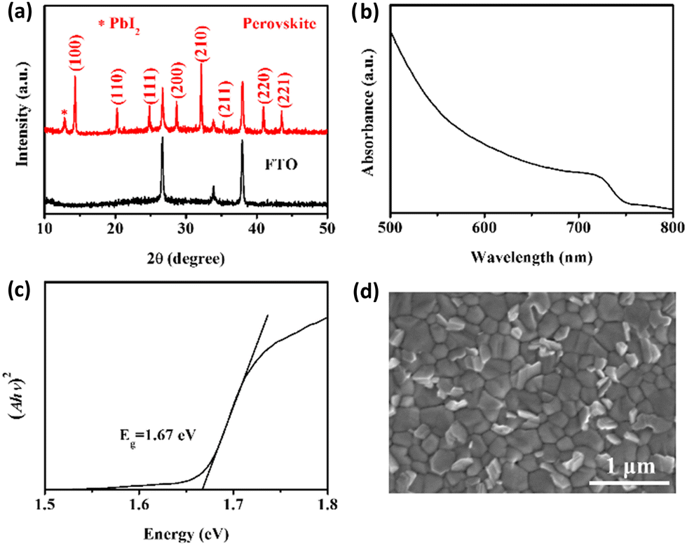 | ||
| Fig. 1 (a) XRD pattern, (b) UV-vis absorption spectrum, (c) Tauc plot and (d) top-view SEM image of the perovskite film. | ||
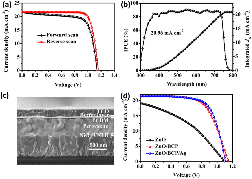 | ||
| Fig. 2 (a) J–V curves (measured in forward and reverse direction scans) and (b) IPCE and integrated Jsc curves of an opaque PSC. (c) Cross-sectional scanning-electric microscopy (SEM) image of an inverted ST-PSC. (d) J–V curves of ST-PSCs with ZnO, ZnO/BCP and ZnO/BCP/Ag buffer layers. | ||
| Buffer layer | V oc (V) | J sc (mA cm−2) | FF (%) | PCE (%) |
|---|---|---|---|---|
| ZnO | 1.10 | 19.17 | 37.42 | 7.88 |
| ZnO/BCP | 1.15 | 21.31 | 63.36 | 15.49 |
| ZnO/BCP/Ag | 1.11 | 21.54 | 67.46 | 16.14 |
In comparison with the corresponding opaque cells, the ST-PSCs show poor PCE, mainly caused by low FF. For further enhancement of the performance of ST-PSCs, a smaller effective area (0.049 cm2) and an additional metal frame were applied to the ST-PSCs to improve the FF by facilitating carrier extraction.45,46 After optimization, the optimal small-area ST-PSC exhibited a forward-scan PCE of 16.39% (Voc: 1.08 V, Jsc: 20.60 mA cm−2, FF: 73.82%) and a reverse-scan PCE of 17.95% (Voc: 1.09 V, Jsc: 20.52 mA cm−2, FF: 80.33%), as shown in Fig. 3a. Fig. 3b shows the IPCE spectrum and the integrated current density obtained from it. There was an obvious decrease in IPCE in the wavelength range from 600 to 700 nm, which might be attributed to inadequate light absorption of the perovskite and high transmittance of the functional layers behind the perovskite (PCBM/ZnO/BCP/Ag/TCO, Fig. 3c).47,48 Also, the value of integrated Jsc (19.97 mA cm−2) was in good agreement with Jsc extracted from the J–V curves, proving the reliability of the J–V measurement. Considering future commercial application of ST-PSCs, a large-area ST-PSC with 1 cm2 effective area was fabricated, yielding a PCE of 15.44% (Fig. S2, ESI†). When the aperture area of mask increased from 0.049 cm2 to 1 cm2, the Jsc of ST-PSC decreased from 20.52 mA cm−2 to 20.36 mA cm−2, the Voc of ST-PSC changed little, and the FF of ST-PSC decreased from 80.33% to 70.21%. These variations might be attributed to the enlarged aperture area and the slightly increased ratio of aperture area/active area (0.51 for 0.049 cm2, 0.64 for 1 cm2).49
 | ||
| Fig. 3 (a) J–V curves in forward and reverse scan directions and (b) IPCE spectrum and integrated Jsc of the optimal small-area ST-PSC. The transmittance curves of (c) different functional layers and (d) filter and MgF2 antireflective layer coated (on glass side) filter. | ||
Transmittance is an important parameter for evaluating the optical loss of functional layers in the device.50Fig. 3c shows variations of the transmittance curve with the addition of functional layers. The transmittance of PCBM was over 90% in the wavelength range of 750–1200 nm, corresponding to a small amount of parasitic absorption. Although an additional film of ZnO nanoparticles on the PCBM reduced the transmittance of light with wavelengths of 500–1200 nm, the relevant difference was smaller than 5%. And for light in the short wavelength range (400–500 nm), the transmittance was even increased after the deposition of the ZnO film. The above-mentioned two phenomena indicated the good transparency of ZnO. The slight difference between the curve of PCBM/ZnO and the curve of PCBM/ZnO/BCP reflected little impact of BCP on the transmittance. In contrast, a significant drop occurred between the transmittance curves of PCBM/ZnO/BCP and PCBM/ZnO/BCP/Ag at wavelengths around 500 nm, indicating that Ag had a strong influence on the transmittance. The transmittance of the PCBM/ZnO/BCP/Ag/TCO combination is crucial to a ST-PSC with light illuminated from the TCO side since the photoactive layer can only absorb the light passed through these layers. A high average transmittance value of 76.35% was obtained for PCBM/ZnO/BCP/Ag/TCO in the wavelength range of 315–1200 nm. Furthermore, the transmittance of a filter including all the functional layers in the ST-PSCs was measured, as shown in Fig. 3d. Its low transmittance for light with wavelengths below 750 nm was mainly attributed to the absorption of the perovskite, and approximately 29% light loss in the wavelength range of 750–1200 nm was ascribed to the parasitic absorption and reflection of the carrier-transport layer, buffer layer, transparent electrode and FTO substrate. To enhance the transmittance of the filter, a 90 nm-thick MgF2 antireflective layer was deposited on the glass side of the filter. Introduction of the MgF2 antireflective layer increased the transmittance of the filter by 1% (800–1200 nm, Fig. 3d). On this basis, evaporating 250 nm of MgF2 on the TCO side further enhanced the transmittance of the filter (Fig. S3, ESI†).
Different measurements were performed to investigate the mechanism responsible for the multi-layer buffer enhancing the photovoltaic performance of these ST-PSCs. Photoluminescence (PL) and time-resolved photoluminescence (TRPL) measurements (Fig. 4a and b) were conducted on samples with a glass/perovskite/PCBM/buffer layer/TCO architecture. The sample with the ZnO/BCP/Ag multi-layer buffer exhibited stronger PL quenching and shorter carrier lifetime (Table S1, ESI†) compared to the other two, indicating faster electron extraction by this structure.51,52 The space-charge-limited-current (SCLC) method (Fig. 4c) was used to investigate the trap-state density in electron-only devices (FTO/TiO2/perovskite/PCBM/buffer layer/TCO/Ag). The trap-state density is proportional to the trap-filled limit voltage (VTFL), which is a turning point between the linear Ohmic region and the nonlinear trap-filling region in the current density–voltage curve.53–55 Among three kinds of devices, the device with the ZnO/BCP/Ag multi-layer buffer presented the smallest VTFL value of 0.122 V, corresponding to the lowest trap-state density and minimum of non-radiative recombination. To sum up, the multi-layer buffer facilitated carrier extraction and reduced non-radiative recombination between the electron transport layer and TCO layer, resulting in the performance improvement of ST-PSCs.
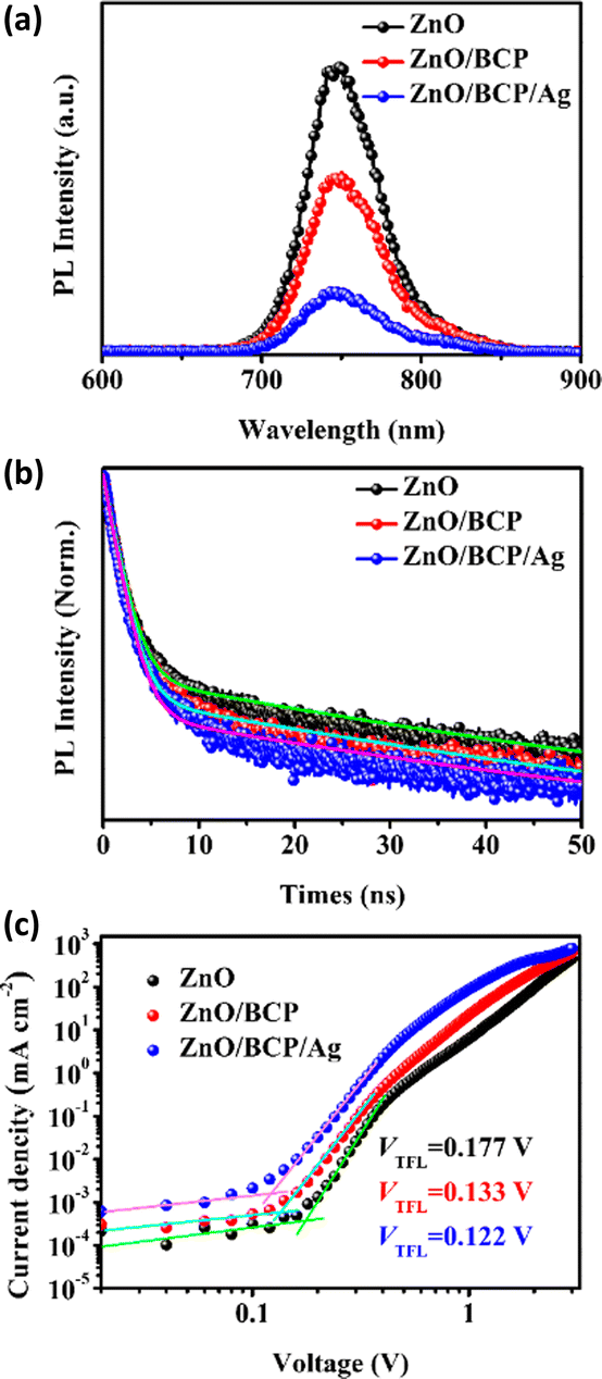 | ||
| Fig. 4 (a and b) PL and TRPL spectra of samples with the configuration glass/perovskite/PCBM/buffer layer/TCO. (c) Current density–voltage curves of electron-only devices. | ||
After the fabrication of efficient ST-PSCs, further tests can be performed to estimate the PCE of an ideal four-terminal perovskite/Si tandem cell. Fig. 5a shows the configuration of the four-terminal tandem device. Adding the PCEs of the ST-PSC and silicon cell filtered by ST-PSC can yield the PCE of the ideal four-terminal tandem cell.56,57 The J–V curves and detailed photovoltaic parameters of the silicon solar cell, filtered silicon cell and ST-PSC are given in Fig. 5b and Table 2. The Jsc loss between the silicon solar cell and the sum of the filtered silicon cell and ST-PSC was as high as 4.28 mA cm−2. Thus, a more effective light management method should be applied for further performance optimization of this kind of tandem device.58,59 According to the data in Table 2, the ideal four-terminal perovskite/Si tandem cell with a PCE of 26.18% was realized by combining a perovskite top cell and a silicon bottom cell. As shown in Fig. 5c, the integrated current densities of the ST-PSC and filtered silicon cell were 19.97 and 15.15 mA cm−2, respectively, approaching the Jsc values derived from the J–V curves. Furthermore, the complementarity of the two IPCE curves in the 600–750 nm range indicated that part of the light passed though the ST-PSC and was absorbed by the bottom silicon cell due to the high transparency of the ST-PSC. The IPCE curve of the filtered silicon cell exhibited similar characteristics to the transmittance curve of the filter in Fig. 3d, in accordance with the actual situation.
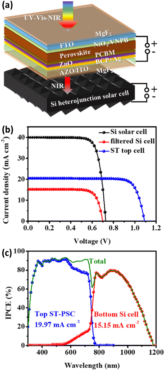 | ||
| Fig. 5 (a) Schematic diagram of the four-terminal perovskite/Si tandem cell. (b) J–V curves and (c) IPCE spectrum of solar cells related to the four-terminal perovskite/Si tandem cell. | ||
| V oc (V) | J sc (mA cm−2) | FF (%) | PCE (%) | |
|---|---|---|---|---|
| ST-PSCs | 1.09 | 20.52 | 80.33 | 17.95 |
| Silicon cell | 0.73 | 40.03 | 77.58 | 22.57 |
| Filtered silicon cell | 0.70 | 15.23 | 77.49 | 8.23 |
| Tandem solar cell | 26.18 |
Conclusions
In conclusion, we have designed and developed a ZnO/BCP/Ag multi-layer buffer, which showed better performances than a single-layer ZnO buffer in eliminating the negative effects of the sputtered electrode. The optimization of the buffer layer enhanced the PCE of ST-PSCs mainly through the improvement of FF, which was realized by reducing non-radiative recombination and accelerating carrier extraction. Furthermore, the ST-PSC and a portion of its functional layers exhibited high transmittance, which is beneficial for light harvesting of the silicon bottom cell and the PCE of the tandem cell. Finally, a ST-PSC with a PCE of 17.95% and a four-terminal perovskite-silicon tandem solar cell with a PCE of 26.18% were obtained. All the above results indicate that utilizing a multi-layer buffer is an effective strategy for performance enhancement of solar cells with sputtered transparent electrodes.Experimental
Materials
Lead iodide (PbI2, 99.999%), lead bromide (PbBr2, 99.999%), cesium iodide (CsI, 99.99%), isopropanol (IPA, anhydrous), N,N-dimethylformamide (DMF, anhydrous), dimethyl sulfoxide (DMSO, anhydrous) and chlorobenzene (CB, anhydrous) were purchased from Youxuan Corp. Ethyl acetate (EA, analytical reagent) was purchased from China National Pharmaceutical Group Corp. Formamidine iodide (FAI, 99.5%), methylammonium bromide (MABr, 99.5%), [6,6]-phenyl C61 butyric acid methyl ester (PCBM, 99%), N4,N4′-di(naphthalen-1-yl)-N4,N4′-bis(4-vinylphenyl)biphenyl-4,4′-diamine (VNPB, 99%) and 2,9-dimethyl-4,7-diphenyl-1,10-phenanthroline (BCP, 99%) were purchased from Xi’an p-OLED Corp. NiO particles were purchased from Beijing Zhongnuo New Technology Corp. Zinc oxide nanoparticle ink was purchased from Sigma-Aldrich Corp. All reagents and materials were used as received without further purification.Device fabrication
Fluorine-doped tin oxide (FTO) substrates were cleaned using deionized water, ethanol and isopropanol and then dried using an air gun. Then, 15 nm of NiOx was deposited on the substrates by electron-beam evaporation. After treatment in oxygen plasma for 3 min, the NiOx-coated substrates were transferred into a N2-filled glove box. 1 mg mL−1 VNPB chlorobenzene solution was spin-coated onto the NiOx-coated substrates at 6000 rpm for 30 s and then annealed at 120 °C for 10 min. After cooling to room temperature, 60 μL perovskite precursor solution was added in droplets onto the substrate and deposited by a one-step spin-coating process (4000 rpm for 35 s). 1.4 M Cs0.05(FA0.77MA0.23)0.95Pb(I0.77Br0.23)3 precursor solution was prepared by dissolving PbI2, PbBr2, FAI, MABr and CsI in a mixture of DMF and DMSO (4![[thin space (1/6-em)]](https://www.rsc.org/images/entities/char_2009.gif) :1 v/v). An additional 5 mg of Pb(SCN)2 was added into the precursor solution to promote grain growth. 13 s before the end of spin-coating, 300 μL ethyl acetate was quickly poured on the film as the anti-solvent. The resulting film was placed on a hotplate at 100 °C for 20 min to form perovskite. For the opaque devices, 20 mg mL−1 PCBM chlorobenzene solution was spun onto the perovskite at 2000 rpm for 30 s, followed by spin-coating of BCP in IPA solution (0.5 mg mL−1) at 4000 rpm for 30 s. 120 nm of Ag was thermally evaporated as the top metal electrode. For the semitransparent devices, PCBM solution (20 mg mL−1) was spun onto the perovskite film at 4000 rpm for 30 s. Then, ZnO nanoparticle ink was deposited using spin-coating (4000 rpm for 30 s) and then annealed at 80 °C for 10 min. Next, a multi-layer buffer was realized by evaporating 8 nm of BCP and 1 nm of Ag in sequence. Finally, common ST-PSCs with an effective area of 0.09 cm2 were obtained by sputtering ITO and AZO at powers of 80 W and 150 W, respectively. The ITO film was deposited with a base pressure of 1 × 10⁻⁵ Torr, a working pressure of 2 × 10⁻³ Torr, a deposition rate of 0.6 Å s−1 and a deposition time of 1200 s. The AZO film was sputtered with a base pressure of 1 × 10⁻⁵ Torr, a working pressure of 2 × 10⁻³ Torr, a deposition rate of 0.8 Å s−1 and a deposition time of 1800 s. To fabricate efficient ST-PSCs with effective areas of 0.049 cm2 or 1 cm2, in addition to the area change of the TCO, a metal frame consisting of a 120 nm-thick Ag layer was thermally evaporated around the TCO. The preparation process of the silicon heterojunction solar cells has been described in a previous report.10 First, potassium hydroxide (KOH) solution was used to etch an n-type silicon wafer to form random pyramids on both sides. After cleaning (the Radio Corporation of America method) and dipping in buffered oxide etching, intrinsic amorphous silicon (a-Si:H) with a thickness of 7 nm was deposited on the surface of silicon wafer by plasma-enhanced chemical vapour deposition. Then, the silicon wafers were treated in hydrogen plasma. Next, p-type a-Si:H (12 nm) and n-type a-Si:H (10 nm) were deposited on the front and rear sides of the silicon wafer, respectively. On the front side of the silicon wafer, after sputtering of ITO (50 nm), a silver grid was fabricated by screen-printing and annealing (200 °C for 20 min), followed by thermally evaporated MgF2 (300 nm). On the rear side of the silicon wafer, ITO (15 nm) and Ag (200 nm) were deposited in sequence by sputtering.
:1 v/v). An additional 5 mg of Pb(SCN)2 was added into the precursor solution to promote grain growth. 13 s before the end of spin-coating, 300 μL ethyl acetate was quickly poured on the film as the anti-solvent. The resulting film was placed on a hotplate at 100 °C for 20 min to form perovskite. For the opaque devices, 20 mg mL−1 PCBM chlorobenzene solution was spun onto the perovskite at 2000 rpm for 30 s, followed by spin-coating of BCP in IPA solution (0.5 mg mL−1) at 4000 rpm for 30 s. 120 nm of Ag was thermally evaporated as the top metal electrode. For the semitransparent devices, PCBM solution (20 mg mL−1) was spun onto the perovskite film at 4000 rpm for 30 s. Then, ZnO nanoparticle ink was deposited using spin-coating (4000 rpm for 30 s) and then annealed at 80 °C for 10 min. Next, a multi-layer buffer was realized by evaporating 8 nm of BCP and 1 nm of Ag in sequence. Finally, common ST-PSCs with an effective area of 0.09 cm2 were obtained by sputtering ITO and AZO at powers of 80 W and 150 W, respectively. The ITO film was deposited with a base pressure of 1 × 10⁻⁵ Torr, a working pressure of 2 × 10⁻³ Torr, a deposition rate of 0.6 Å s−1 and a deposition time of 1200 s. The AZO film was sputtered with a base pressure of 1 × 10⁻⁵ Torr, a working pressure of 2 × 10⁻³ Torr, a deposition rate of 0.8 Å s−1 and a deposition time of 1800 s. To fabricate efficient ST-PSCs with effective areas of 0.049 cm2 or 1 cm2, in addition to the area change of the TCO, a metal frame consisting of a 120 nm-thick Ag layer was thermally evaporated around the TCO. The preparation process of the silicon heterojunction solar cells has been described in a previous report.10 First, potassium hydroxide (KOH) solution was used to etch an n-type silicon wafer to form random pyramids on both sides. After cleaning (the Radio Corporation of America method) and dipping in buffered oxide etching, intrinsic amorphous silicon (a-Si:H) with a thickness of 7 nm was deposited on the surface of silicon wafer by plasma-enhanced chemical vapour deposition. Then, the silicon wafers were treated in hydrogen plasma. Next, p-type a-Si:H (12 nm) and n-type a-Si:H (10 nm) were deposited on the front and rear sides of the silicon wafer, respectively. On the front side of the silicon wafer, after sputtering of ITO (50 nm), a silver grid was fabricated by screen-printing and annealing (200 °C for 20 min), followed by thermally evaporated MgF2 (300 nm). On the rear side of the silicon wafer, ITO (15 nm) and Ag (200 nm) were deposited in sequence by sputtering.
Characterization
The surface and cross-sectional morphologies of the samples were characterized using a field-emission scanning-electron microscope (Hitachi-SU8220). The photovoltaic performance of devices was characterized by a digital source meter (Keithley Model 2400) in air under AM1.5 G simulated solar illumination at 100 mW cm−2 (XES-50S1, SAN-EI). The incident photon-to-electron conversion efficiency (IPCE) spectra were measured on a QE-R Quantum Efficiency Measurement System (Enlitech) in the alternating current mode. For measurement of the four-terminal tandem cell, the silicon cell was tested with a metal aperture (1 cm2) and a 2.5 × 2.5 cm2 filter. The photoluminescence (PL) and time-resolved photoluminescence (TRPL) spectra were acquired by a PicoQuant FluoTime 300 spectrometer (PicoQuant GmbH, Germany). Space-charge-limited-current (SCLC) measurements were performed in the dark using a Keithley 2400 sourcemeter. X-Ray diffraction (XRD) characterization was conducted using an X-ray diffractometer (DX-2700BH, Haoyuan). Ultraviolet-visible (UV-vis) absorption spectra were obtained using a spectrophotometer (Hitachi UH4150). The transmittance curves of the samples were measured using a UV-vis-NIR spectrophotometer (PerkinElmer Lambda 950).Author contributions
Junjie Lou: conceptualization, data curation, investigation and writing-original draft. Jiangshan Feng: conceptualization, supervision, funding acquisition and writing – review & editing. Yang Cao: data curation and resources. Yucheng Liu: formal analysis and data Curation. Yong qin: methodology, validation, supervision and writing – review & editing. Shengzhong (Frank) Liu: project administration, supervision, funding acquisition and writing – review & editing.Conflicts of interest
There are no conflicts to declare.Acknowledgements
The authors acknowledge support from the Fundamental Research Funds for the Central Universities (GK202103106), the Shanxi Science and Technology Department (20201101012), the Strategic Priority Research Program of Chinese Academy of Sciences (Grant No. XDA17040506), the National Natural Science Foundation of China (Grant No. 61975106), the National University Research Fund (Grant No. GK261001009), the Shaanxi Technical Innovation Guidance Project (2018HJCG-17), the Innovative Research Team (Grant No. IRT_14R33), and the 111 Project (Grant No. B14041).Notes and references
- A. Kojima, K. Teshima, Y. Shirai and T. Miyasaka, J. Am. Chem. Soc., 2009, 131, 6050–6051 CrossRef CAS PubMed.
- https://www.nrel.gov/pv/cell-efficiency.html, accessed 2022-12.
- Q. Tai and F. Yan, Adv. Mater., 2017, 29, 1700192 CrossRef PubMed.
- Q. Xue, R. Xia, C. J. Brabec and H.-L. Yip, Energy Environ. Sci., 2018, 11, 1688–1709 RSC.
- G. Giuliano, A. Bonasera, G. Arrabito and B. Pignataro, Sol. RRL, 2021, 5, 2100702 CrossRef CAS.
- K. Araki, Y. Ota and M. Yamaguchi, Appl. Sci., 2020, 10, 872 CrossRef.
- M. Nukunudompanich, D. Sriprapai and S. Sontikaew, Mater. Today Proc., 2022, 66, 3163–3167 CrossRef CAS.
- J. Bing, L. G. Caro, H. P. Talathi, N. L. Chang, D. R. McKenzie and A. W. Y. Ho-Baillie, Joule, 2022, 6, 1446–1474 CrossRef CAS.
- T. M. Koh, H. Wang, Y. F. Ng, A. Bruno, S. Mhaisalkar and N. Mathews, Adv. Mater., 2022, 34, 2104661 CrossRef CAS PubMed.
- Z. Wang, X. Zhu, S. Zuo, M. Chen, C. Zhang, C. Wang, X. Ren, Z. Yang, Z. Liu, X. Xu, Q. Chang, S. Yang, F. Meng, Z. Liu, N. Yuan, J. Ding, S. Liu and D. Yang, Adv. Funct. Mater., 2020, 30, 1908298 CrossRef CAS.
- D. Yang, X. Zhang, Y. Hou, K. Wang, T. Ye, J. Yoon, C. Wu, M. Sanghadasa, S. Liu and S. Priya, Nano Energy, 2021, 84, 105934 CrossRef CAS.
- M. A. Green, E. D. Dunlop, J. Hohl-Ebinger, M. Yoshita, N. Kopidakis, K. Bothe, D. Hinken, M. Rauer and X. Hao, Prog. Photovolt., 2022, 30, 687–701 CrossRef.
- S.-H. Lim, H.-J. Seok, M.-J. Kwak, D.-H. Choi, S.-K. Kim, D.-H. Kim and H.-K. Kim, Nano Energy, 2021, 82, 105703 CrossRef CAS.
- K. Liu, B. Chen, Z. J. Yu, Y. Wu, Z. Huang, X. Jia, C. Li, D. Spronk, Z. Wang, Z. Wang, S. Qu, Z. C. Holman and J. Huang, J. Mater. Chem. A, 2022, 10, 1343–1349 RSC.
- E. Aydin, C. Altinkaya, Y. Smirnov, M. A. Yaqin, K. P. S. Zanoni, A. Paliwal, Y. Firdaus, T. G. Allen, T. D. Anthopoulos, H. J. Bolink, M. Morales-Masis and S. De Wolf, Matter, 2021, 4, 3549–3584 CrossRef CAS.
- P. Löper, S.-J. Moon, S. Martín de Nicolas, B. Niesen, M. Ledinsky, S. Nicolay, J. Bailat, J.-H. Yum, S. De Wolf and C. Ballif, Phys. Chem. Chem. Phys., 2015, 17, 1619–1629 RSC.
- J. Werner, G. Dubuis, A. Walter, P. Löper, S.-J. Moon, S. Nicolay, M. Morales-Masis, S. De Wolf, B. Niesen and C. Ballif, Sol. Energy Mater. Sol. Cells, 2015, 141, 407–413 CrossRef CAS.
- F. Fu, T. Feurer, T. Jäger, E. Avancini, B. Bissig, S. Yoon, S. Buecheler and A. N. Tiwari, Nat. Commun., 2015, 6, 8932 CrossRef CAS PubMed.
- H. H. Park, J. Kim, G. Kim, H. Jung, S. Kim, C. S. Moon, S. J. Lee, S. S. Shin, X. Hao, J. S. Yun, M. A. Green, A. W. Y. Ho-Baillie, N. J. Jeon, T.-Y. Yang and J. Seo, Small Methods, 2020, 4, 2000074 CrossRef CAS.
- E. Aydin, J. Liu, E. Ugur, R. Azmi, G. T. Harrison, Y. Hou, B. Chen, S. Zhumagali, M. De Bastiani, M. Wang, W. Raja, T. G. Allen, A. U. Rehman, A. S. Subbiah, M. Babics, A. Babayigit, F. H. Isikgor, K. Wang, E. Van Kerschaver, L. Tsetseris, E. H. Sargent, F. Laquai and S. De Wolf, Energy Environ. Sci., 2021, 14, 4377–4390 RSC.
- J. A. Raiford, R. A. Belisle, K. A. Bush, R. Prasanna, A. F. Palmstrom, M. D. McGehee and S. F. Bent, Sustain. Energy Fuels, 2019, 3, 1517–1525 RSC.
- D. P. McMeekin, G. Sadoughi, W. Rehman, G. E. Eperon, M. Saliba, M. T. Hörantner, A. Haghighirad, N. Sakai, L. Korte, B. Rech, M. B. Johnston, L. M. Herz and H. J. Snaith, Science, 2016, 351, 151–155 CrossRef CAS PubMed.
- R. A. Jagt, T. N. Huq, S. A. Hill, M. Thway, T. Liu, M. Napari, B. Roose, K. Gałkowski, W. Li, S. F. Lin, S. D. Stranks, J. L. MacManus-Driscoll and R. L. Z. Hoye, ACS Energy Lett., 2020, 5, 2456–2465 CrossRef CAS.
- K. Jäger, L. Korte, B. Rech and S. Albrecht, Opt. Express, 2017, 25, A473–A482 CrossRef PubMed.
- F. Fu, T. Feurer, T. P. Weiss, S. Pisoni, E. Avancini, C. Andres, S. Buecheler and A. N. Tiwari, Nat. Energy, 2016, 2, 16190 CrossRef.
- Y. H. Jang, J. M. Lee, J. W. Seo, I. Kim and D.-K. Lee, J. Mater. Chem. A, 2017, 5, 19439–19446 RSC.
- Q. Han, Y.-T. Hsieh, L. Meng, J.-L. Wu, P. Sun, E.-P. Yao, S.-Y. Chang, S.-H. Bae, T. Kato, V. Bermudez and Y. Yang, Science, 2018, 361, 904–908 CrossRef CAS PubMed.
- E. Aydin, M. De Bastiani, X. Yang, M. Sajjad, F. Aljamaan, Y. Smirnov, M. N. Hedhili, W. Liu, T. G. Allen, L. Xu, E. Van Kerschaver, M. Morales-Masis, U. Schwingenschlögl and S. De Wolf, Adv. Funct. Mater., 2019, 29, 1901741 CrossRef.
- K. A. Bush, S. Manzoor, K. Frohna, Z. J. Yu, J. A. Raiford, A. F. Palmstrom, H.-P. Wang, R. Prasanna, S. F. Bent, Z. C. Holman and M. D. McGehee, ACS Energy Lett., 2018, 3, 2173–2180 CrossRef CAS.
- F. Sahli, J. Werner, B. A. Kamino, M. Bräuninger, R. Monnard, B. Paviet-Salomon, L. Barraud, L. Ding, J. J. Diaz Leon, D. Sacchetto, G. Cattaneo, M. Despeisse, M. Boccard, S. Nicolay, Q. Jeangros, B. Niesen and C. Ballif, Nat. Mater., 2018, 17, 820–826 CrossRef CAS PubMed.
- B. Chen, Z. Yu, K. Liu, X. Zheng, Y. Liu, J. Shi, D. Spronk, P. N. Rudd, Z. Holman and J. Huang, Joule, 2019, 3, 177–190 CrossRef CAS.
- K. A. Bush, A. F. Palmstrom, Z. J. Yu, M. Boccard, R. Cheacharoen, J. P. Mailoa, D. P. McMeekin, R. L. Z. Hoye, C. D. Bailie, T. Leijtens, I. M. Peters, M. C. Minichetti, N. Rolston, R. Prasanna, S. Sofia, D. Harwood, W. Ma, F. Moghadam, H. J. Snaith, T. Buonassisi, Z. C. Holman, S. F. Bent and M. D. McGehee, Nat. Energy, 2017, 2, 17009 CrossRef CAS.
- D. H. Kim, C. P. Muzzillo, J. Tong, A. F. Palmstrom, B. W. Larson, C. Choi, S. P. Harvey, S. Glynn, J. B. Whitaker, F. Zhang, Z. Li, H. Lu, M. F. A. M. van Hest, J. J. Berry, L. M. Mansfield, Y. Huang, Y. Yan and K. Zhu, Joule, 2019, 3, 1734–1745 CrossRef CAS.
- J. Xu, C. C. Boyd, Z. J. Yu, A. F. Palmstrom, D. J. Witter, B. W. Larson, R. M. France, J. Werner, S. P. Harvey, E. J. Wolf, W. Weigand, S. Manzoor, M. F. A. M. van Hest, J. J. Berry, J. M. Luther, Z. C. Holman and M. D. McGehee, Science, 2020, 367, 1097–1104 CrossRef CAS PubMed.
- Z. Ying, Y. Zhu, X. Feng, J. Xiu, R. Zhang, X. Ma, Y. Deng, H. Pan and Z. He, Adv. Mater. Interfaces, 2021, 8, 2001604 CrossRef CAS.
- Z. Ying, X. Yang, J. Zheng, Y. Zhu, J. Xiu, W. Chen, C. Shou, J. Sheng, Y. Zeng, B. Yan, H. Pan, J. Ye and Z. He, J. Mater. Chem. A, 2021, 9, 12009–12018 RSC.
- Y. Bai, X. Meng and S. Yang, Adv. Energy Mater., 2018, 8, 1701883 CrossRef.
- C. Chen, S. Zhang, S. Wu, W. Zhang, H. Zhu, Z. Xiong, Y. Zhang and W. Chen, RSC Adv., 2017, 7, 35819–35826 RSC.
- X. Liu, P. Huang, Q. Dong, Z. Wang, K. Zhang, H. Yu, M. Lei, Y. Zhou, B. Song and Y. Li, Sci. China: Chem., 2017, 60, 136–143 CrossRef CAS.
- M. S. Selim, A. M. Elseman and Z. Hao, ACS Appl. Energy Mater., 2020, 3, 11781–11791 CrossRef CAS.
- A. Al-Ashouri, E. Köhnen, B. Li, A. Magomedov, H. Hempel, P. Caprioglio, J. A. Márquez, A. B. Morales Vilches, E. Kasparavicius, J. A. Smith, N. Phung, D. Menzel, M. Grischek, L. Kegelmann, D. Skroblin, C. Gollwitzer, T. Malinauskas, M. Jošt, G. Matič, B. Rech, R. Schlatmann, M. Topič, L. Korte, A. Abate, B. Stannowski, D. Neher, M. Stolterfoht, T. Unold, V. Getautis and S. Albrecht, Science, 2020, 370, 1300–1309 CrossRef CAS PubMed.
- Z. Liu, J. Chang, Z. Lin, L. Zhou, Z. Yang, D. Chen, C. Zhang, S. Liu and Y. Hao, Adv. Energy Mater., 2018, 8, 1703432 CrossRef.
- B. Zhang, J. Su, X. Guo, L. Zhou, Z. Lin, L. Feng, J. Zhang, J. Chang and Y. Hao, Adv. Sci., 2020, 7, 1903044 CrossRef CAS PubMed.
- L. Zhou, J. Su, Z. Lin, X. Guo, J. Ma, T. Li, J. Zhang, J. Chang and Y. Hao, Research, 2021, 2021, 9836752 CAS.
- E. Köhnen, M. Jošt, A. B. Morales-Vilches, P. Tockhorn, A. Al-Ashouri, B. Macco, L. Kegelmann, L. Korte, B. Rech, R. Schlatmann, B. Stannowski and S. Albrecht, Sustain. Energy Fuels, 2019, 3, 1995–2005 RSC.
- M. J. Jeong, J. H. Lee, C. H. You, S. Y. Kim, S. Lee and J. H. Noh, Adv. Energy Mater., 2022, 12, 2200661 CrossRef CAS.
- N. Li, F. Meng, F. Huang, G. Yu, Z. Wang, J. Yan, Y. Zhang, Y. Ai, C. Shou, Y. Zeng, J. Sheng, B. Yan and J. Ye, ACS Appl. Energy Mater., 2020, 3, 9610–9617 CrossRef CAS.
- H. Wang, H. A. Dewi, T. M. Koh, A. Bruno, S. Mhaisalkar and N. Mathews, ACS Appl. Mater. Interfaces, 2020, 12, 484–493 CrossRef CAS PubMed.
- C. Tong, W. Ji, D. Li, A. Mei, Y. Hu, Y. Rong and H. Han, J. Mater. Chem. A, 2019, 7, 10942–10948 RSC.
- N. N. Lal, Y. Dkhissi, W. Li, Q. Hou, Y.-B. Cheng and U. Bach, Adv. Energy Mater., 2017, 7, 1602761 CrossRef.
- A. Peter Amalathas, L. Landová, K. Ridzoňová, L. Horák, P. Bauerová and J. Holovský, ACS Appl. Energy Mater., 2021, 4, 11488–11495 CrossRef CAS.
- Y.-N. Zhang, B. Li, L. Fu, Q. Li and L.-W. Yin, Electrochim. Acta, 2020, 330, 135280 CrossRef CAS.
- H. Yi, D. Wang, M. A. Mahmud, F. Haque, M. B. Upama, C. Xu, L. Duan and A. Uddin, ACS Appl. Energy Mater., 2018, 1, 6027–6039 CrossRef CAS.
- Y. Xie, J. Feng, M. Chen, X. Zhu, Y. Zhou, Z. Li, D. Yang and S. Frank Liu, ACS Appl. Energy Mater., 2022, 5, 8034–8041 CrossRef CAS.
- Y. Zhou, A. Najar, J. Zhang, J. Feng, Y. Cao, Z. Li, X. Zhu, D. Yang and S. F. Liu, ACS Appl. Mater. Interfaces, 2022, 14, 28729–28737 CrossRef CAS PubMed.
- T. Duong, N. Lal, D. Grant, D. Jacobs, P. Zheng, S. Rahman, H. Shen, M. Stocks, A. Blakers, K. Weber, T. P. White and K. R. Catchpole, IEEE J. Photovolt., 2016, 6, 679–687 Search PubMed.
- J. Werner, B. Niesen and C. Ballif, Adv. Mater. Interfaces, 2018, 5, 1700731 CrossRef.
- Q. Xu, Y. Zhao and X. Zhang, Sol. RRL, 2020, 4, 1900206 CrossRef.
- D. A. Jacobs, M. Langenhorst, F. Sahli, B. S. Richards, T. P. White, C. Ballif, K. R. Catchpole and U. W. Paetzold, J. Phys. Chem. Lett., 2019, 10, 3159–3170 CrossRef CAS PubMed.
Footnote |
| † Electronic supplementary information (ESI) available. See DOI: https://doi.org/10.1039/d2ma01089e |
| This journal is © The Royal Society of Chemistry 2023 |