
 Open Access Article
 This Open Access Article is licensed under a
 Creative Commons Attribution 3.0 Unported Licence
Rational design of 2D/2D CS/SiC van der Waals type-II heterojunctions: a visible-light-driven photocatalyst for hydrogen production
Francis
Opoku
 *,
Osei
Akoto
,
Edward Ebow
Kwaansa-Ansah
,
Noah Kyame
Asare-Donkor
and
Anthony Apeke
Adimado
*,
Osei
Akoto
,
Edward Ebow
Kwaansa-Ansah
,
Noah Kyame
Asare-Donkor
and
Anthony Apeke
Adimado
Department of Chemistry, Kwame Nkrumah University of Science and Technology, Kumasi, Ghana. E-mail: ofrancis2010@gmail.com; francisopoku@knust.edu.gh
First published on 21st March 2023
Abstract
A hotspot in renewable energy research is visible-light-driven photocatalytic water splitting for hydrogen production. Monolayer stacking in the form of van der Waals heterojunctions (vdWHs) can be used for band gap engineering and the control of exciton dynamics for prospective nano-electronic devices. Using state-of-the-art hybrid dispersion-corrected density functional theory calculations (DFT-D3(BJ)), 2D/2D CS/SiC vdWHs are designed and investigated for the feasibility of using them as a potential photocatalyst for visible-light-driven H2 generation. It has been established that the most favourable stacking pattern of CS/SiC vdWHs is mechanically, dynamically, and energetically stable, paving the way for their experimental synthesis. Furthermore, the charge transfer at the interface area generates a built-in electric field that may be used to prevent electron–hole recombination, which is favourable for achieving increased carrier mobility and prolonged lifetimes. Additionally, the CS/SiC vdWHs show a maximum optical absorption intensity for visible light, reaching 105 cm−1, and a suitable band gap (1.96 eV) that crosses the redox potentials of photocatalytic water splitting at pH = 7. A positive electric field (+0.6 to +0.8 V Å−1) and a negative electric field (−0.2 to −0.6 V Å−1) can be used to tune the band alignment of CS/SiC vdWHs to type I, offering theoretical guidance for their experimental synthesis for applying them in next-generation optoelectronics and solar energy devices. These results provide comprehensive knowledge of the enhanced photocatalytic mechanism of 2D/2D CS/SiC vdWHs, and they also offer a rational method for developing very effective CS/SiC photocatalysts for H2 production.
I. Introduction
Global energy demands and consumption have exponentially increased over the past few years due to a significant increase in industrialization, urbanization and population.1 Despite extensive research into conventional fossil fuels to meet energy demand, their usage is harmful to the environment due to the emission of CO2 and other greenhouse gases, such as NH3 and CH4. The global energy supply is heavily dependent on fossil fuels, and intensification of environmental concerns and rapid depletion of fossil fuels drive the necessity to research alternative zero-emission and eco-friendly energy resources.2 Among the available alternative energy sources and fuels, hydrogen (H2) has emerged as a desirable renewable energy resource to replace existing fossil fuels since only water is produced during H2 combustion3 and it possesses a high energy density per unit mass.4 Technologies for conversion and storage are required to produce H2 effectively and in a sustainable manner. Currently, large-scale H2 production employs the CO2-producing process of steam reforming of fossil fuels.5 A possible green chemistry strategy to meet future energy demands is the direct conversion of water into clean and sustainable H2 energy powered by solar light through photocatalytic water splitting.6,7Previously, electrocatalysts based on noble metals, such as iridium, ruthenium or platinum were the benchmark materials for H2 production in electrolysers.8 The extensive use of these noble metals in water electrolysis is strongly constrained by their scarcity and high cost. As energy sources fail to keep up with the rising worldwide demand, research on effective visible-light-driven photocatalysts for water splitting has accelerated. Due to their hexagonal symmetry, tunable band gaps, and unique electronic, mechanical, and optical properties, two-dimensional (2D) materials have received much attention in materials chemistry and have been thoroughly investigated as potential photocatalysts for efficient next-generation H2 production.9,10 Among all the 2D materials, silicon carbide (SiC) has emerged as an auspicious material for effective H2 evolution due to its electronic, structural, mechanical, magnetic and optical properties.11–13 SiC with a unique 2D planar graphene-like structure can be used in harsh environments, such as environments with strong thermal stability and in-plane stiffness.14 It has been confirmed that isolated SiC is theoretically stable.15 Recently, SiC monolayers with a unique 2D planar graphene-like geometry have been reported to be theoretically stable, having high carrier mobility and direct bandgap properties.16 These properties make 2D SiC a promising material for photovoltaic and optoelectronic applications, such as diodes and solar cells.17 On the other hand, the performance of 2D SiC monolayers in solar energy harvesting is constrained by their broad band gap energy, particularly in the visible light range. Furthermore, it is challenging to use a single semiconductor as a photocatalyst for water splitting due to the short lifespan of photogenerated charge carriers, which allows for quick recombination of photoexcited electron–hole pairs.3
Several researchers have investigated vertical heterostructures generated by stacking two distinct 2D monolayer materials that localize the conduction band minimum (CBM) and valence band maximum (VBM) via van der Waals (vdW) forces instead of covalent bonds to address the issue of fast recombination of charge carriers.18,19 An efficient method to boost the efficiency of 2D photocatalysts for water splitting is to build heterostructures.20,21 Moreover, vdW heterojunctions (vdWHs) in particular may integrate the isolated features of the constituent monolayers and fine-tune the electronic structures.22 Furthermore, 2D vdWHs with type-II band structures may efficiently split water into oxygen and hydrogen because 2D materials offer a wide surface area for the photogenerated charge carriers to come into contact with each other.23,24 Type-II semiconducting vdWHs are the most beneficial for sunlight harvesting and utilization because they accelerate the spatial separation of photogenerated carrier pairs.25,26 Numerous theoretical and experimental studies have demonstrated the capacity of 2D type-II vdWHs not only in modifying the band structures to straddle water redox potentials but also in enhancing the separation of charge carriers to reduce recombination.27 To enhance the photocatalytic efficiency, several SiC-based vdWHs, such as SiC/C2N,28 XSSe/SiC (X = Mo or W),29 boron phosphide/SiC,30 SiS/SiC,31 SiC/MoS2,32 SiC/g-C3N4,33 SiC/MoSSe,34 SiC/BS,35 blue phosphorene/SiC36 and BlueP/SiC3 have been investigated.37 Monolayer silicon and germanium monochalcogenides (i.e., SiS, SiSe, GeS and GeSe) have been found to be suitable for overall photocatalytic water splitting.38,39 Another class of 2D materials, XY (X = C, Si, Ge, or Sn; Y = O, S, Se, or Te) which exhibit planar structures,40 have attracted much attention due to their stable configuration.41 The planar, buckling and puckered structures are three different possible geometrical configurations for each of these 2D binary monolayers.42 The favoured hybridization in group V monolayers (arsenene and phosphorene) is sp3, but the hexagonal planar structure favours sp2 hybridization, showing that the hybridization in group IV–VI binary monolayers is comparable to that of arsenene and phosphorene.42 Due to the intense overlap of the conduction and valence bands, it has been found that CS monolayers in the planar configuration are metallic.40 Inspired by these, carbon sulphide (CS) was predicted to be a highly efficient photocatalyst for water splitting with a high carrier mobility (3.23 × 104 cm2 V−1 s−1) and a moderate band gap (2.41![[thin space (1/6-em)]](https://www.rsc.org/images/entities/char_2009.gif) eV), comparable to those of other newly reported 2D photocatalysts.43 Additionally, CS is found to exhibit a substantial intrinsic dipole (0.43 D), which enables the introduction of a built-in internal electric field that can efficiently promote the separation of photogenerated carriers.43 The design of CS/SiC vdWHs has been possible as a result of structural investigation of 2D CS and SiC, which revealed that they both share a honeycomb structure with a little lattice mismatch.44
eV), comparable to those of other newly reported 2D photocatalysts.43 Additionally, CS is found to exhibit a substantial intrinsic dipole (0.43 D), which enables the introduction of a built-in internal electric field that can efficiently promote the separation of photogenerated carriers.43 The design of CS/SiC vdWHs has been possible as a result of structural investigation of 2D CS and SiC, which revealed that they both share a honeycomb structure with a little lattice mismatch.44
The rational design and scalable fabrication of stable and highly active noble-metal-free photocatalysts for effective H2 generation have been one of the solutions for an industry-scale and speedy application of H2 generation technology for clean and sustainable energy production. Advanced solar energy devices frequently make use of the type-II band alignment created by limiting the VBM and CBM to two different layers of vdWHs because it can change the interlayer transition energy. According to earlier research, forming a heterostructure with a lattice mismatch (η) of <5% is beneficial.45 Based on their excellent electronic properties and small η, CS/SiC vdWHs are constructed by stacking CS and SiC monolayers through weak vdW contact. A small η value can ensure experimental synthesis of CS/SiC vdWHs and help investigate their viability as an efficient material for water splitting. Here, density functional theory calculations are performed to analyse the potential drop, charge density difference, position of the Fermi energy level, and electronic band gap (Eg) of CS/SiC vdWHs with potential for application in water splitting reactions via the hydrogen evolution reaction (HER). Four stacking configurations are examined and identified the most stable system through calculations of thermodynamic stability. The dynamic and thermal stabilities are addressed where favourable heterostructures are chosen. Furthermore, the ability of the oxidation–reduction process to convert water into H2 and O2 at pH 0–14 is assessed.
II. Computational details
All the calculations (i.e., electronic properties and periodic 2D slab) were performed using the density functional theory-based Quantum Espresso suite code.46 The optimised norm-conserving Vanderbilt pseudopotentials47 and generalized gradient approximation (GGA) of Perdew–Burke–Ernzerhof (PBE) were used to explain the core-electron and exchange–correlation functional,48 respectively. A plane-wave basis set with a kinetic energy cutoff of 40 Ry was used to extend the Kohn–Sham orbitals and the 15 × 15 × 1 k-point grids of Monkhorst–Pack49 in the Brillouin zone (BZ) were sampled. Interactions between the periodic boundary conditions were prevented by using a 25 Å vacuum space along the z-axis. The total electronic energy (Hellmann–Feynman force) of the calculated systems in the self-consistent loop was converged to 10−8 Ry (10−3 Ry bohr−1). The computationally expensive Heyd–Scuseria–Ernzerhof functional50 was used to obtain accurate electronic and optical properties, which are often underestimated by the PBE functional. The separation parameter (μ = 0.20 Å−1) and the mixing parameter (α = 0.25) were set to their default levels. The Grimme DFT-D3(BJ) dispersion approach51,52 is acceptable for all simulations since the vdW interaction is anticipated to be significant in influencing the physical characteristics and dynamics of layered structures.53 The ab initio molecular dynamics (AIMD) calculations were run using an NVT ensemble at 300, 500, and 800 K for 100 ps to evaluate the thermodynamic stability of CS/SiC vdWHs. All AIMD simulations were carried out using the Car–Parrinello code based on Quantum Espresso.46 During AIMD simulations, a 4 × 4 × 1 supercell was used to accommodate lattice translation constraints. Within the Quantum Espresso code,46 the phonon dispersion calculations were performed using density functional perturbation theory. The phonon dispersion curve was computed on a 10 × 10 × 1 q point grid. The vibrational modes at the Γ-point were calculated using the acoustic sum rule.Additionally, the interface binding energies (Eb) of the four heterostructures were determined using the following equation to assess the stability of the structure:
| Eb = (ECS/g-SiC − ECS − Eg-SiC)/A, | (1) |
The following equation was used to calculate the charge density difference (Δρ) of the CS/SiC vdWH along the direction perpendicular to the plane (z-direction):
| Δρ = ρCS/SiC − ρCS − ρSiC, | (2) |
The optical absorption properties were obtained by calculating the dielectric function (ε(ω)) as follows:54
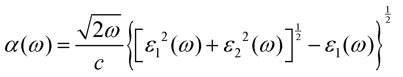 | (3) |
III. Results and discussion
In this study, the geometrical structures and electronic properties of isolated CS and SiC monolayers are initially investigated before constructing the CS/SiC vdWHs. Fig. 1(a) and (d), respectively, depict the geometrical and electronic characteristics of monolayers made of CS and SiC.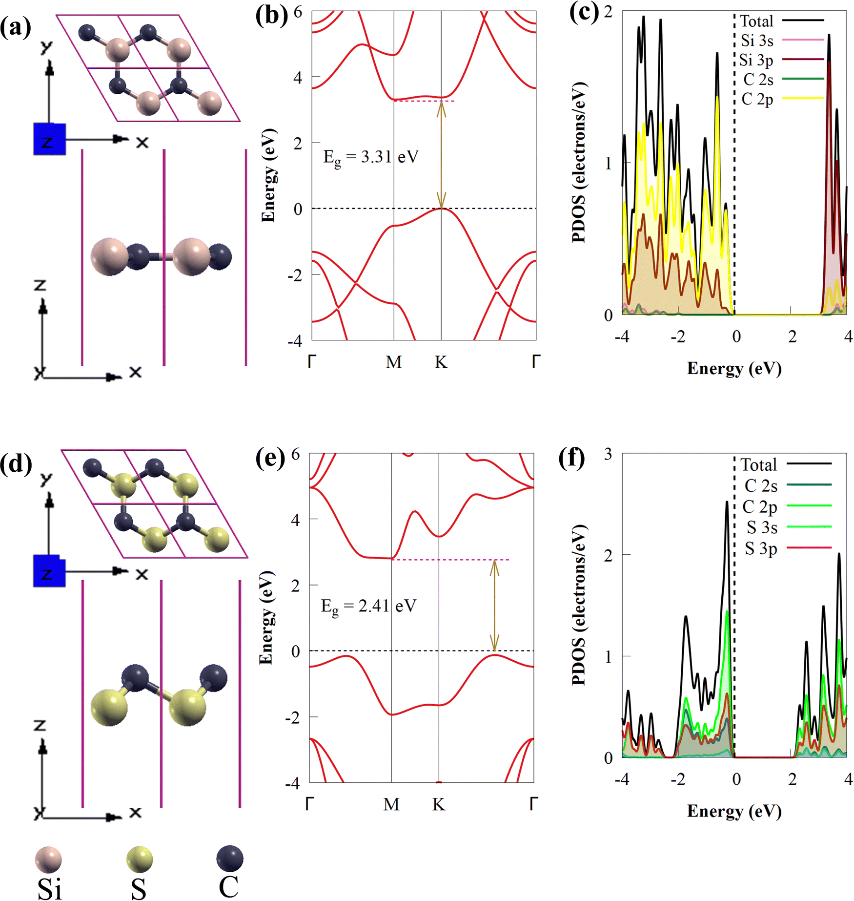 | ||
| Fig. 1 The (a) geometry, (b) band structure and (c) projected density of states of SiC monolayers. The (d) geometry, (e) band structure and (f) projected density of states of the CS monolayer. The Fermi level is set to zero for clarity. | ||
Both CS and SiC have optimized lattice constants of a = b = 2.825 and 3.094 Å, respectively, which result in hexagonal lattices that are in agreement with previous findings (3.09 Å55 and 2.82 Å).43 The computed band structure for the SiC monolayer reveals that the Si–C bond length is about 1.787 Å and that it is a semiconductor with an indirect Eg of 3.31 eV, with its CBM situated at the M point and VBM situated at the K point (Fig. 1(b)). Its Eg, however, is too broad to absorb photons from the visible region. These findings agree with those of earlier reports.28,56 According to the partial density of states (PDOS) of SiC, there is significant orbital mixing between the C-p and Si-p orbitals, with the VBM being derived mostly from Si-p states and the CBM derived from C-p states. An important drawback of SiC monolayers in photocatalysts is the lack of efficient separation of charge carriers due to electron transfer occurring on the same atom at the active sites. The aforementioned findings support earlier research showing that SiC is unsuitable as a visible-light-driven photocatalyst. The isolated CS monolayer exhibits an indirect band gap (2.41 eV), similar to the SiC monolayer, with its CBM at the M point, while the VBM is along the K → Γ path. After optimization, the C–S bond length of monolayer CS is predicted to be 1.873 Å. In addition, the VBN and CBM mainly originate from C 2p states. The calculated indirect band gap and C–S bond length of the CS monolayer agree well with prior experimental and theoretical findings.43
When considering a material as a vdWH, the η value is another crucial factor to consider.57 The formation of a vdWH is made simple by the transfer of a 2D monolayer onto a 2D crystal substrate.58η is calculated as follows:59
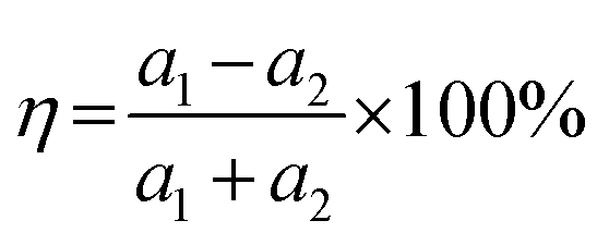 | (4) |
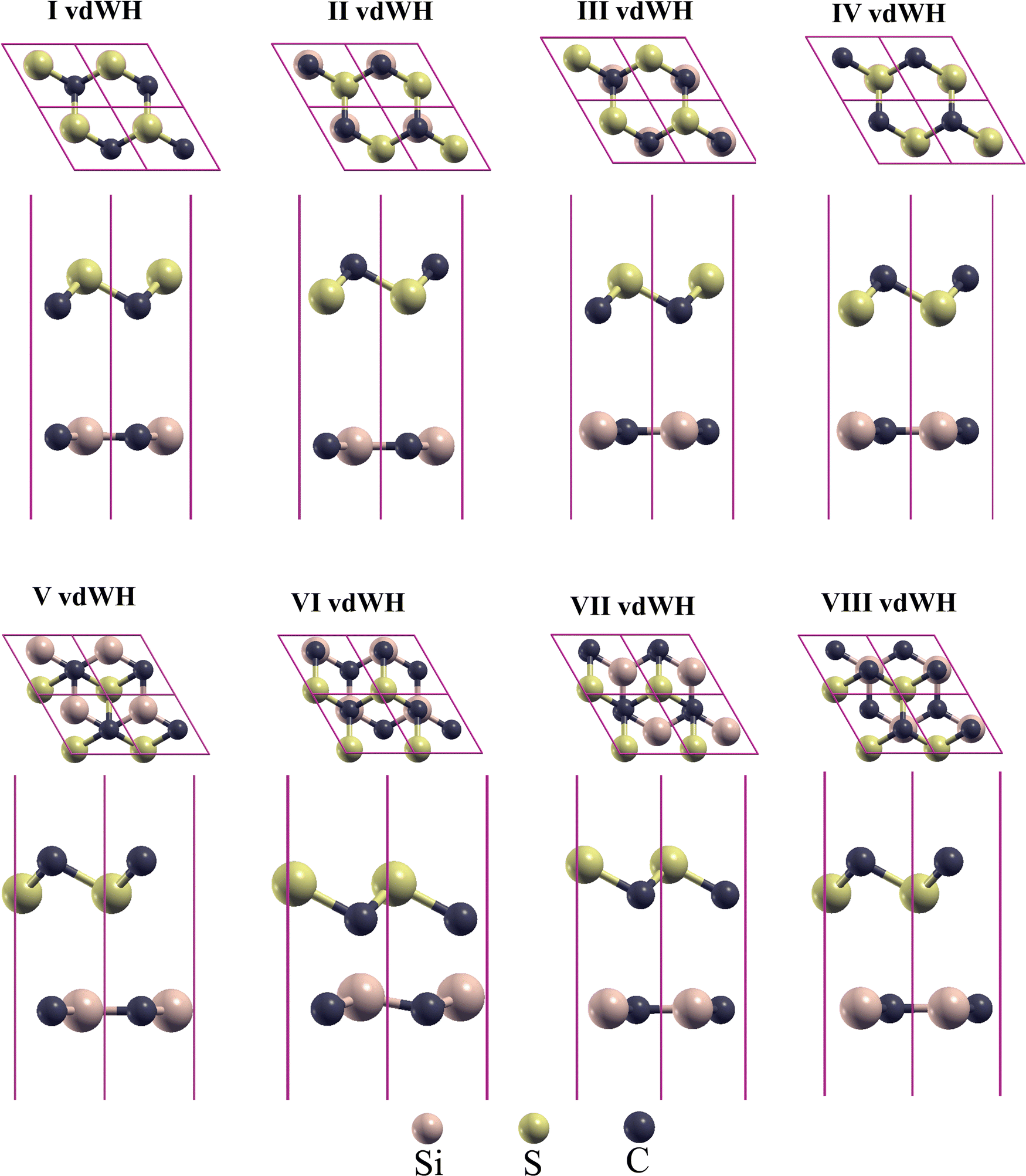 | ||
| Fig. 2 Optimized structures of CS/SiC vdWHs in four different stacking patterns. The lower layer shows the side view and the upper layer denotes a top view. | ||
The optimised structures of CS/SiC vdWHs are illustrated in Fig. 2. The CS and SiC monolayers retain their original planar structure after optimization, demonstrating that the interaction between CS and SiC monolayers is vdW force rather than chemical covalent bonds. Some selected crucial parameters regarding these several stacking configurations of CS/SiC vdWHs are given in Table 1.
| System | a (Å) | E b (meV Å−2) | d (Å) | Φ (eV) | ΔV (eV) | E g (eV) | Charge (e) |
|---|---|---|---|---|---|---|---|
| SiC | 3.094 | — | — | 5.01 | — | 3.31 | — |
| CS | 2.825 | — | — | 5.46 | — | 2.41 | — |
| I vdWH | 3.016 | −9.040 | 4.153 | 4.59 | 0.76 | 0.48 | 0.0032 |
| II vdWH | 3.019 | −14.389 | 3.799 | 4.85 | 1.81 | 1.96 | 0.0096 |
| III vdWH | 3.017 | −6.751 | 4.024 | 4.31 | 0.69 | 0.51 | 0.0036 |
| IV vdWH | 3.018 | −11.225 | 3.847 | 4.92 | 1.59 | 2.01 | 0.0052 |
| V vdWH | 3.016 | −10.304 | 3.905 | 5.20 | 1.87 | 2.23 | 0.0046 |
| VI vdWH | 3.019 | −9.423 | 4.080 | 4.86 | 0.99 | 1.88 | 0.0054 |
| VII vdWH | 3.017 | −10.592 | 3.825 | 4.94 | 0.71 | 1.09 | 0.0042 |
| VIII vdWH | 3.018 | −8.674 | 4.010 | 6.06 | 1.85 | 2.39 | 0.0066 |
The interlayer distance, which is recommended to be in the range of 3–4 Å,62 is one of the criteria for determining whether a material may be used to form vdWHs. From Table 1 the interactions of all the configurations are weak because of the wide interlayer separation. The stability of a 2D heterostructure is always determined using the binding energy as an effective approach.32 The Eb value of the stacking patterns is listed in Table 1. The Eb value is predicted to be negative, pointing to the configurations of CS/SiC vdWHs being energetically favourable. According to the binding energy, the II vdWH pattern is the most stable stacking configuration. Thus, the II vdWH stacking pattern is selected as a representative to investigate the electronic and optical properties of CS/SiC vdWHs.
Thermal stability is crucial from the standpoint of applications. The final structure of CS/SiC vdWHs is still preserved after 100 ps of heating at 300, 500 and 800 K, as shown in insets in Fig. 3(b)–(d). This illustrates how the thermal process in the CS/SiC vdWH did not result in geometric reconstruction or chemical bond breaking. Additionally, as shown in Fig. 3(b)–(d), the results of the AIMD simulations reveal that there are few temperature and energy fluctuations, indicating that the thermal stable structure is under an equilibrium condition at 300, 500 and 800 K.
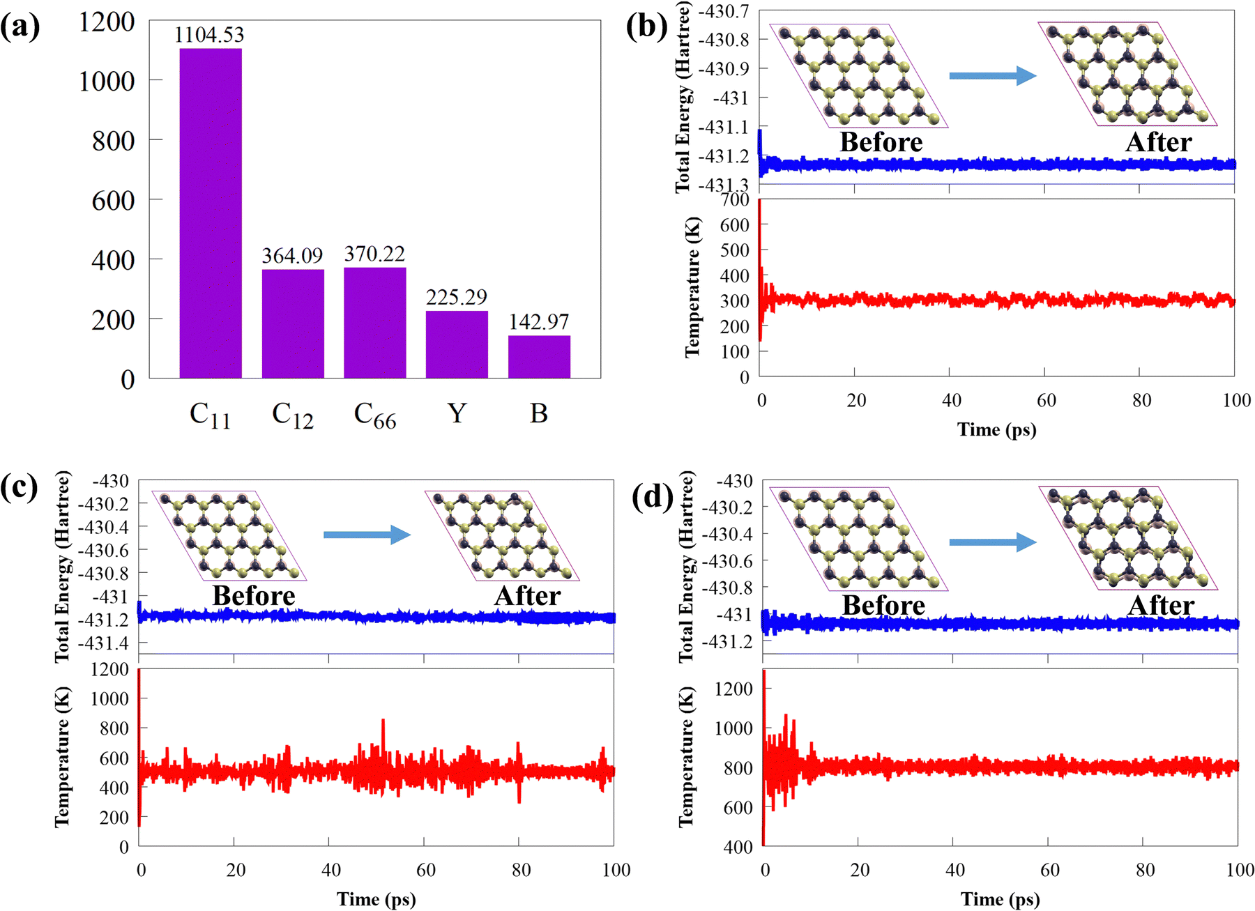 | ||
| Fig. 3 (a) The histogram of the calculated 2D elastic modulus (N m−1) and constants. Variation of temperature and total potential energy across a time scale of 100 ps at (b) 300 K, (c) 500 K and (d) 800 K. The insets represent snapshots of the atomic structure of 4 × 4 supercells of CS/SiC vdWHs at temperatures of 300, 500 and 800 K. | ||
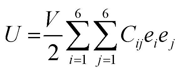
Due to the significance of mechanical flexibility in 2D materials, the curvature of the energy–strain relationship, as represented in the Thermo_pw code,63 has been used to determine the elastic constants (Cij). When exposed to in-plane strains, the CS/SiC vdWH possess sufficient mechanical stability. Elastic constants may be calculated using the energy–strain relationship in the linear elastic limit64,65 in terms of elastic constants and ideal strengths as follows:
 | (5) |
Additionally, as shown in Fig. 4, a phonon dispersion spectrum is used to analyse the lattice dynamic stability of CS and SiC monolayers and CS/SiC vdWHs. The spectrum had positive frequencies in the whole BZ, indicating that the CS/SiC vdWHs show very strong dynamic stability, ensuring their successful fabrication.
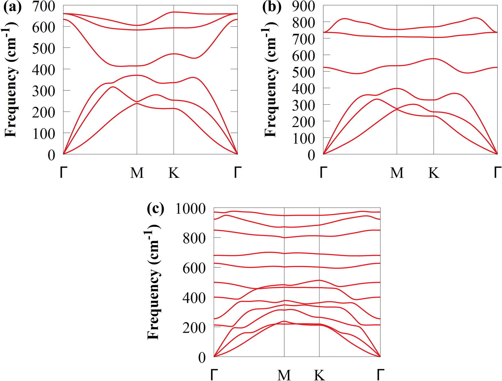 | ||
| Fig. 4 The calculated phonon dispersion spectra of (a) CS, (b) SiC and (c) CS/SiC vdWHs. | ||
The electronic structure of the CS/SiC vdWH is then investigated. The properties of the CS and SiC monolayers are well conserved following the design of the vdWH, as illustrated in Fig. 5(a). The indirect Eg value of the CS/SiC vdWH, which is defined by the differences in the VBM and CBM at the K and M points, is 1.96 eV when the stacking II pattern is taken into account. Due to the type-II band alignment that is created from each of the separate monolayers during the contact process, the CS/SiC vdWH has a significantly lower Eg value (1.96 eV) than either the CS (2.41 eV) or SiC (3.31 eV) monolayer. This suggests that in CS/SiC vdWHs, the electron transfer becomes simpler. It is generally known that a photocatalyst should have an ideal Eg value of ∼2 eV56 to absorb enough visible light to initiate a photocatalytic redox reaction. According to the PDOS shown in Fig. 5(b), the CS and SiC monolayers dominate the CBM and VBM, respectively. In contrast to the CBM, which is equally dominated by the C-p and S-p orbitals of the CS monolayer, the VBM is primarily contributed by the C-p orbitals of the SiC monolayer with a minor contribution from the Si-p orbitals.
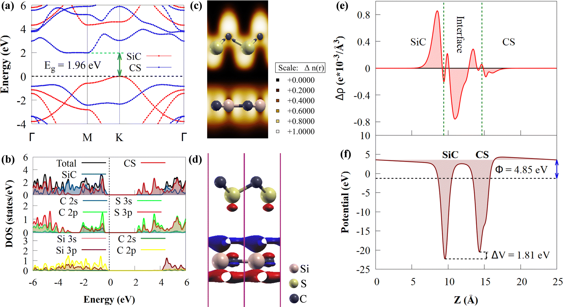 | ||
| Fig. 5 (a) Projected band structures, (b) PDOS and (c) electron localization function plot of CS/SiC vdWH. (d) Side view of the three-dimensional and (e) the macroscopic planar averaged charge density difference of CS/SiC vdWHs; the isosurface is set to 0.0006 e bohr−3. The blue (red) colour represents the loss (gain) of electrons. (f) The macroscopic planar averaged electrostatic potential along the z direction of CS/SiC vdWHs. | ||
The three-dimensional (3D) charge density difference (CDD) and the corresponding planar-average CDD along the z direction are calculated, to explore the interlayer interactions and gain a fundamental understanding of the improved photocatalytic performance of CS/SiC vdWHs. A negative value (blue colour) represents charge depletion, while a positive value (red colour) represents charge accumulation, as shown in Fig. 5(d). The findings demonstrate that charge transfer took place at the interface as a result of the interaction of the CS and SiC monolayers. The macroscopic planar averaged charge density difference shown in Fig. 5(e) establishes that the SiC monolayer donates electrons to the CS monolayer. In Table 1, charge analysis demonstrates that about 0.0096 e is being transferred from SiC monolayers to CS monolayers. As a result, the electric field (Ef) created by the charge transfer between the two types of materials acts as a driving force to stop the fast recombination of photoexcited charge carriers at the interface of CS and SiC monolayers.70 A weak contact between the SiC and CS monolayers is indicated by the small charge transfer, which is consistent with the calculations for the SiC(GeC)/MoS2 heterostructure.70 For further information, the electron localization function (ELF)71 of the CS/SiC vdWH is computed to validate the presence of the vdW force between the CS and SiC monolayers, as given in Fig. 5(c). The work functions of the CS and SiC monolayers, and the CS/SiC vdWH are 5.46, 5.01 and 4.85 eV, respectively. Due to the considerably higher work function of the CS monolayer than that of the SiC monolayer, electrons move from the SiC monolayer to the CS monolayer when they come into close contact. At the heterojunction interface, a built-in Ef is created due to charge transfer. With a potential drop (ΔV) of 1.81 eV at the interface, it can be seen that the SiC monolayer has a deeper potential than the CS monolayer, suggesting that electrons have transferred from the SiC monolayer to the CS monolayer. Moreover, ΔV serves as a transport barrier between adjacent monolayers and can greatly change the charge transport in 2D vdWHs.72 When the heterostructure is utilized in solar conversion devices, the ΔV at the CS/SiC vdWH interface creates an electrostatic field that could prevent photogenerated electron–hole pairs from recombining.37
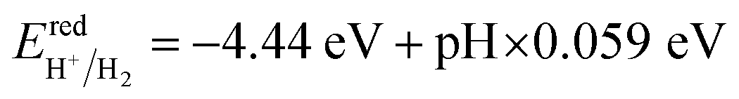
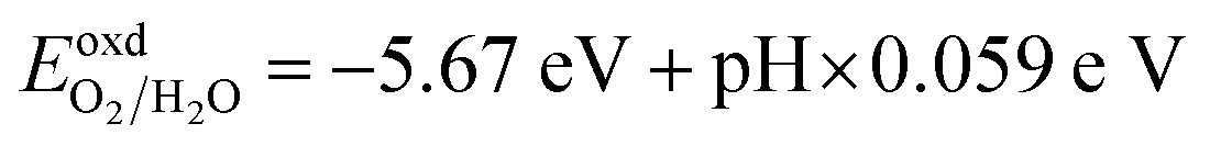
Understanding how well the CS/SiC vdWH performs as a photocatalyst for splitting water into H2 requires a study of the suitable band edges that straddle the redox potentials of water splitting. By selecting the vacuum level as the reference, the reduction potential for producing H2 and oxidation potential for O2 generation have been reported to be −4.44 eV (H+/H2) and −5.67 eV (O2/H2O) at pH = 0, respectively.73 A semiconductor with appropriate CBM and VBM potentials is required for thermodynamically advantageous water redox processes. Additionally, they must all fall within a minimum band gap value of 1.23 eV. The positions of the VBMs and CBMs of the corresponding materials are evaluated as follows:74
| EVBM = −I = −χ − 0.5 × Eg | (6) |
| ECBM = −A = −χ + 0.5 × Eg | (7) |
 | ||
| Fig. 6 (a) Schematic illustration of the band edge potentials against a normal hydrogen electrode at pH = 0 of CS, SiC and CS/SiC vdWHs. (b) Band alignments of CS/SiC vdWHs at different pH values. (c) The calculated absorption spectra of CS, SiC and CS/SiC vdWHs. The calculated Gibbs free energy diagram of the HER for a hydrogen atom absorbed on the (c) SiC- and (d) CS-side of CS/SiC vdWHs, T = 298.15 K. | ||
It is discovered that the oxidation and reduction potentials of water splitting are involved inside the band edges of an isolated SiC monolayer, suggesting that the material has exceptional photocatalytic activity. A wide band gap and quick charge carrier recombination of the isolated SiC photocatalyst may also make it challenging to drive the hydrogen evolution process. Moreover, the isolated SiC photocatalyst could struggle to drive the hydrogen evolution reaction because of its wide band gap and rapid charge carrier recombination. The VBM of SiC must thus be adjusted to straddle the hydrogen and oxygen potentials. The CS/SiC vdWH exhibits a typical type II band alignment since its calculated CBM value is −0.567 eV, lower than the reduction potential of water, while its predicted VBM is 1.393 eV, higher than the oxidation potential of water. The potential of CS/SiC vdWHs for photocatalytic hydrogen generation is further demonstrated by the fact that they can be used to split water under neutral conditions. The conduction band offset (CBO) and valence band offset (VBO) of CS/SiC vdWHs are both around 0.82 eV and 0.73 eV, respectively. Then, photogenerated electrons transfer from the conduction band of SiC to CS, with the CBO, while photogenerated holes transfer from the valence band of CS to SiC with the help of VBO. A type II band alignment is also advantageous for separating the charge carriers produced by photons. The acid–base properties of the environment in which the photocatalyst materials are applied, show a significant impact on the photocatalytic performances. Therefore, by altering the pH values, the effects of acid–base characteristics on the photocatalytic activity of CS/SiC vdWH are examined. The oxidation and reduction potentials of water at various pH levels are computed as follows:32
 | (8) |
 | (9) |
Fig. 6(b) shows that the CS/SiC vdWH may achieve a perfect balance between the oxidation and reduction potentials of water splitting on altering the pH value from 0 (strong acid) to 3 (relatively weak acid) and finally to 7 (neutral); this shows that the photocatalytic performance is improved. The fact that the band edges of CS/SiC vdWHs are situated at energetically advantageous locations indicates that this material may split water when operating at pH values between 0 and 7. Similar to blue phosphorene/BSe21 and GaTe/C2N76 vdWH photocatalysts, the CBMs of CS/SiC vdWHs are closer to the reduction potential at pH = 7. This suggests that water splitting activities are more advantageous in a relatively weak acidic environment.
The Gibbs free-energy for hydrogen adsorption (ΔGH) is a major descriptor for determining the HER activity for a wide variety of photocatalysts.26,77–79 Calculating the HER activity is crucial because a high electrocatalytic activity for the HER process is important to increase the photocatalytic efficiency. The hydrogen adsorption energy (ΔEH) is defined as follows:80
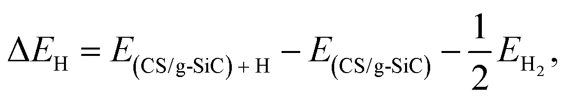 | (10) |
| ΔGH* = ΔEH + ΔEZPE − TΔSH | (11) |
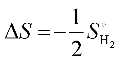 | (12) |
 is the entropy of H2 gas under standard conditions. For the hydrogen adsorption study, ΔEZPE − TΔSH = 0.24 eV is taken from an earlier report.82 Hence, ΔEZPE − TΔSH = 0.24 eV was used in the present study. Catalysts with a high +ΔGH* value result in weak hydrogen adsorption, which further reduces the HER activity. Equally, a high −ΔGH* value results in the formation of strong hydrogen atom bonds on the surface of the catalyst, which results in poor HER activity.83,84 Therefore, for excellent HER activity, the optimal value of ΔGH* should be zero or near-zero. As proposed in previous studies, a ΔGH* range of +0.3 to 0.3 −eV is chosen to test the accessibility of the reaction sites for HER activity.85,86 To study the hydrogen adsorption on the surface of CS/SiC vdWHs, a 3 × 3 supercell is adopted. Moreover, several sites are considered for hydrogen adsorption on the basal plane of the CS/SiC surface. In this study, there are two conditions of a hydrogen atom adsorbed on the plane of the SiC-side and CS-side, as shown in Fig. 6(c) and (d). The reaction rate will be limited if hydrogen atoms cannot be swiftly adsorbed on the surface of the heterojunction and will have an impact on how the HER proceeds. The ΔGH* values are all close to zero and fall in the HER active region (+0.3 eV ≥ ΔGH ≥ −0.3 eV), which implies that it is feasible for CS/SiC vdWHs to achieve the HER. Additionally, the HER is more effective when the hydrogen atom is adsorbed on a Si atom; hence Si atoms are thought of as active sites that are favourable for the HER. The Gibbs free energy of this system is better than those of GeC/MoSi2N487 and C3N/WS2 heterojunctions;79 therefore the properties of CS/SiC vdWHs are more superior. In summary, the CS/SiC vdWH performs the HER well, and its capacity for photocatalytic water splitting of hydrogen has been further confirmed.
Wide and powerful optical absorption edges and intensity are essential components to achieve high photoactivity for water splitting. The absorption spectra of the combined effects of CS and SiC monolayers, and CS/SiC vdWHs, are computed to investigate the visible-light absorption edge and intensity. By comparing the optical absorption spectra of CS and SiC monolayers, the CS monolayer is found to have a greater optical absorption edge and intensity, as shown in Fig. 6(e). Remarkably, the absorption coefficient of CS/SiC vdWHs has improved thanks to the enhanced visible light activity of the CS monolayer, laying the foundation for the development of solar-driven photocatalysts. The exciton splitting caused by the inherent Ef at the interface is the cause of the red-shift absorption. As a result, the broadening of the visible light absorption spectrum supports the idea that CS/SiC vdWHs might be a possible choice for photocatalytic devices.
The ability of Ef and strain to influence the electronic properties of 2D materials is widely understood. In experiments, changing the gate voltage can also be used to adjust the electronic properties of 2D materials. The electronic structures of CS/SiC vdWHs will experience intriguing effects as a result of the external Ef. Here, the electronic properties are considered by using Ef between −0.8 to 0.8 V Å−1 in the vertical direction. The direction of the electric field from SiC monolayer to the CS monolayer is where the positive Ef is applied. Fig. 7(b) and (c) depicts how the band gap energies and band structure vary when an external Ef between −0.8 and 0.8 V Å−1 is applied.
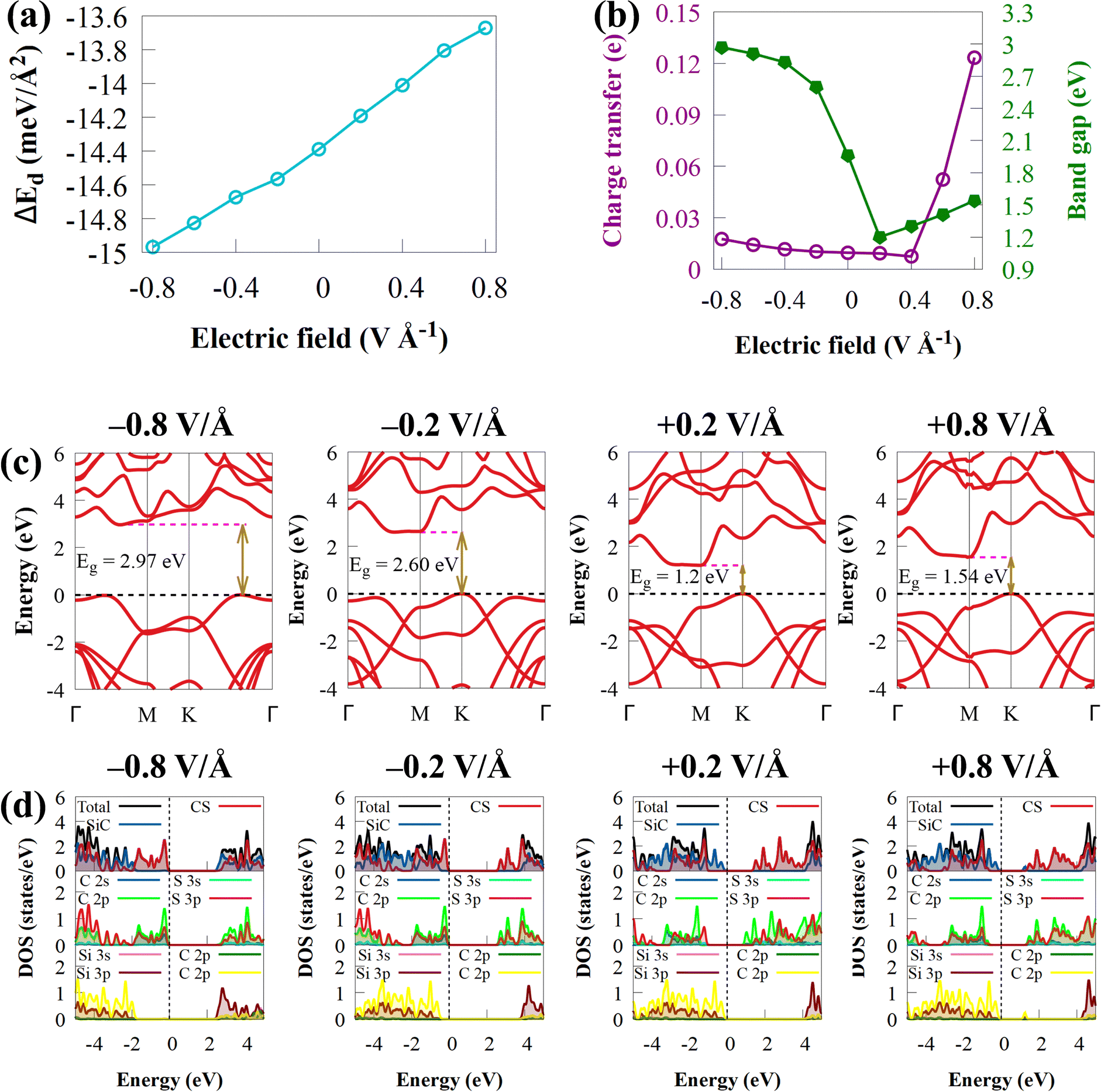 | ||
| Fig. 7 (a) Evolution of interface binding energy of CS/SiC vdWHs under different electric fields. (b) Band gap and charge transfer variations in relation to the external electric field. (c) The electronic band structure and (d) total and partial density of state of CS/SiC vdWH under the effect of negative (−0.8 and −0.2 V Å−1) and positive (0.2 and 0.8 V Å−1) electric fields using the HSE06 method. | ||
The curvature of Eg with external Ef shown in Fig. 7(b) suggests that the Eg value of CS/SiC vdWHs differs a lot under different external Ef. The Eg value of CS/SiC vdWHs is found to increase with an increase in the negative Ef value (−0.2 to −0.8 V Å−1) but decreases when a positive Ef value (+0.2 V Å−1) is introduced before increasing once again from +0.4 to +0.8 V Å−1. Moreover, the found energies are still lower than the Eg value under an Ef of 0 V Å−1. When the applied Ef is in the range of −0.2 to +0.8 V Å−1, the CS/SiC vdWH behaves as an indirect Eg material with the location of the CBM and VBM along the BZ remaining unchanged. It is an indirect Eg material with an Eg value in the range of −0.4 to −0.8 V Å−1; however, the CBM and VBM have different positions; the CBM changes from the M point to lie between Γ and M points, while the VBM changes from the K point to lie between K and Γ points. The type-II band alignment may be maintained within this range, according to Fig. 7(d), which shows that the VBM and CBM are provided by SiC and CS, respectively, with an applied Ef from +0.2 to +0.4 V Å−1 and under −0.8 V Å−1. However, under a positive electric field of +0.6 to +0.8 V Å−1 and a negative electric field of −0.2 to −0.6 V Å−1, the CS/SiC vdWH belongs to the type-I band alignment because the CBM and VBM are both dominated by SiC and CS monolayers, respectively, as presented in Fig. 7. Thus, the interconversion between type-II and type-I can be achieved by applying different electric fields. All these findings suggest that the novel CS/SiC vdWH has significant application prospects in next-generation photovoltaic and photocatalytic devices.
The influence of biaxial strain (ε) on the electronic properties of the CS/SiC vdWH, taking into account the effects of the induced strain caused by both the lattice mismatch and the vdW interaction, is considered. By changing the lattice constants along the a- and b-axes, it is possible to examine the influence of ε on the electronic properties of CS/SiC vdWHs:
 | (13) |
| Es = TE(ε) − TE(ε=0) | (14) |
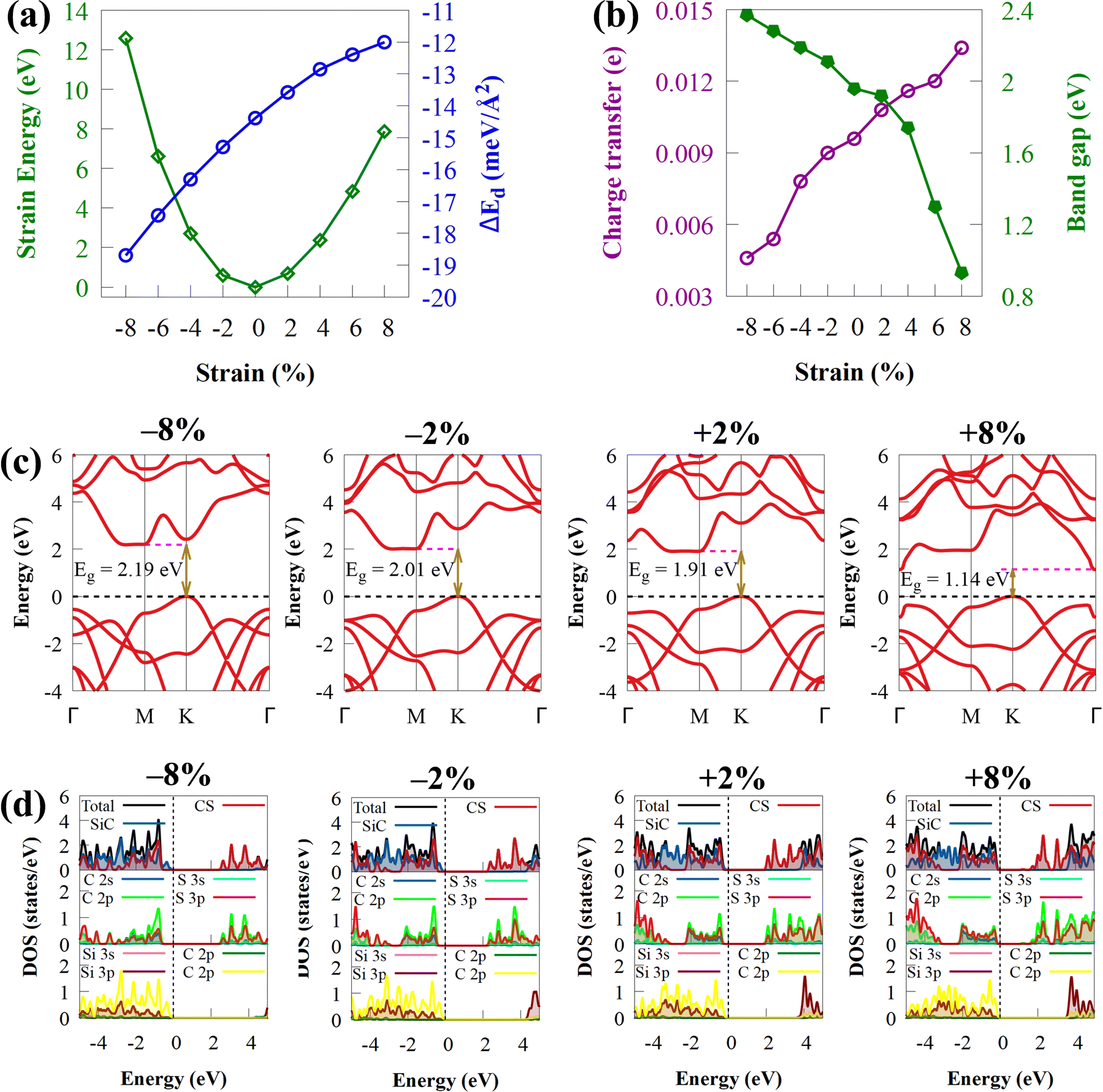 | ||
| Fig. 8 (a) Evolution of the strain energy and interface binding energy of CS/SiC vdWHs under a biaxial strain of −8% to 8%. (b) The band gap energies and charge transfer of CS/SiC vdWHs under a biaxial strain of −8% to 8%. (c) The electronic band structure and (d) total and partial density of state of CS/SiC vdWHs under the effect of biaxial compressive (−2% and −8%) and tensile (2% and 8%) strains using the HSE06 method. | ||
Biaxial strain engineering is one of the most effective methods to modify the band structure of many 2D materials and improve their electronic properties.89Fig. 8(b) shows the effect of biaxial strain on the Eg energies of CS/SiC vdWHs. The predicted Eg of CS/SiC vdWH under the strain effect with the HSE06 functional are in the range of 0.93 to 2.37 eV, as shown in Fig. 8(b), indicating that this material could absorb a large portion of solar radiation. The band gap is lowered when the tensile biaxial strain rises, and the indirect band gap is still maintained, as seen in Fig. 8(c). This is because more charge is being transferred at the interface between the CS and SiC monolayers. The Eg decreases with increasing tensile strain due to a significant reduction in the localization of electrons and an increase in atom covalence. However, the Eg energy increases with the compressive strain, and it is noted that the changes in the tensile strains (0.93 eV (at 8%) to 1.92 eV (at 2%)) are larger than those in the compression strain (2.11 eV (at −2%) to 2.37 eV (at −8%)), where the increase in the band gap energy is lower than the decrease in tensile strain. When compressive strain is used, the ionic properties are enhanced. The distribution of electrons gets increasingly confined as the coupling effect between orbitals weakens. Due to this, the band gap energy increases as the compressive strain increases. An indirect Eg of 0.93 eV under a biaxial strain of about 8% makes it unsuitable for water splitting but suitable for optoelectronic applications. When the tensile strain is increased from 4% to 8%, the CBM at the M point moves to the Γ point, while the VBM remains unchanged, which still makes it an indirect bandgap semiconductor (Fig. 8(c)). Moreover, the band gap is indirect under a compressive strain of −2 to −8%. As a demonstration, PDOS of CS/SiC vdWH against biaxial strains has been selected, as shown in Fig. 8(d). When biaxial strains of −8% to 8% are applied to CS/SiC vdWHs, SiC and CS, respectively, contribute to the VBM and CBM, keeping the properties of the type-II band alignment. The peaks associated with the orbitals participating in the VBM and CBM can be seen changing and extending in Fig. 8(d) because the DOS is directly related to the modification of Eg caused by strain. The height of the peaks in the PDOS is decreased/increased under compressive/tensile biaxial strain.
IV. Conclusion
Several typical 2D/2D CS/SiC vdWHs with various stacking patterns are considered to evaluate the underlying processes and to give a systematic method for developing effective visible-light-driven photocatalysts for H2 generation. Four CS/SiC vdWH structures are built using various stacking techniques. The most stable stacking pattern of CS/SiC vdWHs is considered by comparing the total energy of several stacking patterns. The feasibility and performance of CS/SiC vdWHs are also studied. Our calculations reveal that CS/SiC vdWHs are dynamically, energetically, chemically and mechanically stable and could be experimentally synthesised. The electron localization functions confirmed the interlayer vdW contact. The isolated CS and SiC monolayer materials may attain the type II band alignment with an indirect Eg of 1.96 eV, demonstrating that the oxidation (H2O → O2) and reduction (2H+ → H2) reactions will occur on different monolayers. The CS/SiC vdWHs can efficiently separate the photogenerated charge carriers thanks to the type-II band alignment, where the CBM is provided by the CS monolayer and the VBM is donated by the SiC monolayer. The plane-average electrostatic potentials show that SiC possesses a deeper potential of 1.81 eV than the CS monolayer. This indicates the establishment of a large interfacial built-in Ef, which can prevent the photogenerated charge carriers from recombining. The band edge alignment of CS/SiC vdWHs has the right potential energy to split water into H+/H2 and O2/H2O at pH 7. More significantly, the excellent visible light activity of CS allows the CS/SiC vdWH to significantly broaden the optical absorption range and improve the absorption capability of SiC up to 105 cm−1. Also, the band alignment type of CS/SiC vdWHs can be transformed between type-II and type-I by adjusting the positive electric field (+0.4 to +0.8 V Å−1) and the negative electric field (−0.2 to −0.6 V Å−1). Finally, the hydrogen adsorption on a Si atom has the smallest −ΔGH* when calculating the catalytic activity of the HER. Therefore, we predict that the novel CS/SiC vdWHs have high application prospects in next-generation photovoltaic and photocatalytic devices.Conflicts of interest
The authors declare that they have no known competing financial interests or personal relationships that could have appeared to influence the work reported in this paper.Acknowledgements
We acknowledge the computational support provided by the Centre for High Performance Computing (CHPC), Cape Town.References
- Bhawna, S. Kumar, R. Sharma, A. Gupta, A. Tyagi, P. Singh, A. Kumar and V. Kumar, New J. Chem., 2022, 46, 4014–4048 RSC.
- T. R. Cook, D. K. Dogutan, S. Y. Reece, Y. Surendranath, T. S. Teets and D. G. Nocera, Chem. Rev., 2010, 110, 6474–6502 CrossRef CAS PubMed.
- K. Ren, C. Ren, Y. Luo, Y. Xu, J. Yu, W. Tang and M. Sun, Phys. Chem. Chem. Phys., 2019, 21, 9949–9956 RSC.
- J. Lee, S. Kang, K. Yim, K. Y. Kim, H. W. Jang, Y. Kang and S. Han, J. Phys. Chem. Lett., 2018, 9, 2049–2055 CrossRef CAS PubMed.
- J. A. Turner, Science, 2004, 305, 972–974 CrossRef CAS PubMed.
- W.-J. Yin, B. Wen, C. Zhou, A. Selloni and L.-M. Liu, Surf. Sci. Rep., 2018, 73, 58–82 CrossRef CAS.
- J. Su, Y. Wei and L. Vayssieres, J. Phys. Chem. Lett., 2017, 8, 5228–5238 CrossRef CAS PubMed.
- V. R. Stamenkovic, D. Strmcnik, P. P. Lopes and N. M. Markovic, Nat. Mater., 2017, 16, 57–69 CrossRef CAS PubMed.
- D.-J. Xue, S.-C. Liu, C.-M. Dai, S. Chen, C. He, L. Zhao, J.-S. Hu and L.-J. Wan, J. Am. Chem. Soc., 2017, 139, 958–965 CrossRef CAS PubMed.
- M. J. Allen, V. C. Tung and R. B. Kaner, Chem. Rev., 2010, 110, 132–145 CrossRef CAS PubMed.
- S. Li, M. Sun, J.-P. Chou, J. Wei, H. Xing and A. Hu, Phys. Chem. Chem. Phys., 2018, 20, 24726–24734 RSC.
- A. Hao, X. Yang, X. Wang, Y. Zhu, X. Liu and R. Liu, J. Appl. Phys., 2010, 108, 063531 CrossRef.
- Y. Ma, Y. Dai, M. Guo, C. Niu, L. Yu and B. Huang, Appl. Surf. Sci., 2011, 257, 7845–7850 CrossRef CAS.
- P. Ivanov and V. Chelnokov, Semicond. Sci. Technol., 1992, 7, 863 CrossRef CAS.
- C. L. Freeman, F. Claeyssens, N. L. Allan and J. H. Harding, Phys. Rev. Lett., 2006, 96, 066102 CrossRef PubMed.
- S. Chabi, H. Chang, Y. Xia and Y. Zhu, Nanotechnology, 2016, 27, 075602 CrossRef PubMed.
- H. Şahin, C. Ataca and S. Ciraci, Appl. Phys. Lett., 2009, 95, 222510 CrossRef.
- K. Ren, S. Wang, Y. Luo, J.-P. Chou, J. Yu, W. Tang and M. Sun, J. Phys. D: Appl. Phys., 2020, 53, 185504 CrossRef CAS.
- T. Roy, M. Tosun, X. Cao, H. Fang, D.-H. Lien, P. Zhao, Y.-Z. Chen, Y.-L. Chueh, J. Guo and A. Javey, ACS Nano, 2015, 9, 2071–2079 CrossRef CAS PubMed.
- F. Opoku, A. Aniagyei, O. Akoto, E. E. Kwaansa-Ansah, N. K. Asare-Donkor and A. A. Adimado, Mater. Adv., 2022, 3, 4629–4640 RSC.
- B.-J. Wang, X.-H. Li, R. Zhao, X.-L. Cai, W.-Y. Yu, W.-B. Li, Z.-S. Liu, L.-W. Zhang and S.-H. Ke, J. Mater. Chem. A, 2018, 6, 8923–8929 RSC.
- J. Katoch, S. Ulstrup, R. J. Koch, S. Moser, K. M. McCreary, S. Singh, J. Xu, B. T. Jonker, R. K. Kawakami and A. Bostwick, Nat. Phys., 2018, 14, 355–359 Search PubMed.
- F. Opoku, O. Akoto, S. O.-B. Oppong and A. A. Adimado, New J. Chem., 2021, 45, 20365–20373 RSC.
- H. Wang, L. Zhang, Z. Chen, J. Hu, S. Li, Z. Wang, J. Liu and X. Wang, Chem. Soc. Rev., 2014, 43, 5234–5244 RSC.
- F. Opoku, S. O.-B. Oppong, N. K. Asare-Donkor, O. Akoto and A. A. Adimado, Energy Adv., 2022, 1, 146–158 RSC.
- Y.-L. Liu, Y. Shi and C.-L. Yang, Appl. Surf. Sci., 2021, 545, 148952 CrossRef CAS.
- D. Deng, K. Novoselov, Q. Fu, N. Zheng, Z. Tian and X. Bao, Nat. Nanotechnol., 2016, 11, 218–230 CrossRef CAS PubMed.
- L. Xu, Z. Ma, Q. Li, T. Chen, B. Peng, J. Zeng, Y. Zhang, K.-W. Luo, L.-L. Wang and C. Shuai, New J. Chem., 2020, 44, 15439–15445 RSC.
- Z. Cui, K. Bai, Y. Ding, X. Wang, E. Li and J. Zheng, Phys. E, 2020, 123, 114207 CrossRef CAS.
- T.-N. Do, M. Idrees, B. Amin, N. N. Hieu, H. V. Phuc, N. V. Hieu, L. T. Hoa and C. V. Nguyen, RSC Adv., 2020, 10, 32027–32033 RSC.
- Q. Alam, S. Muhammad, M. Idrees, N. V. Hieu, N. T. T. Binh, C. Nguyen and B. Amin, RSC Adv., 2021, 11, 14263–14268 RSC.
- X. Gao, Y. Shen, Y. Ma, S. Wu and Z. Zhou, Phys. Chem. Chem. Phys., 2019, 21, 15372–15379 RSC.
- L. Xu, Q. Li, X.-F. Li, M.-Q. Long, T. Chen, B. Peng, L.-L. Wang, Y. Yang and C. Shuai, Catal. Sci. Technol., 2019, 9, 3896–3906 RSC.
- D. Qin, X. Zhang, W. Li, K. Wang and S. Wang, Superlattices Microstruct., 2021, 153, 106837 CrossRef CAS.
- H. Li, H. Zhang, Y. Xiong, L. Ye and W. Li, Phys. Lett. A, 2021, 410, 127514 CrossRef CAS.
- J. Ni, M. Quintana, F. Jia and S. Song, Phys. E, 2021, 127, 114460 CrossRef CAS.
- H. Din, M. Idrees, G. Rehman, C. V. Nguyen, L.-Y. Gan, I. Ahmad, M. Maqbool and B. Amin, Phys. Chem. Chem. Phys., 2018, 20, 24168–24175 RSC.
- L. Sun, Y. Cui, L. Peng, J. Du, S. Wang and Y. Huang, J. Catal., 2019, 373, 67–74 CrossRef CAS.
- D. Gu, X. Tao, H. Chen, W. Zhu, Y. Ouyang and Q. Peng, Nanoscale, 2019, 11, 2335–2342 RSC.
- C. Kamal, A. Chakrabarti and M. Ezawa, Phys. Rev. B, 2016, 93, 125428 CrossRef.
- G. Ding, G. Gao and K. Yao, Sci. Rep., 2015, 5, 9567 CrossRef CAS PubMed.
- H. Khan, M. U. Ashraf, M. Idrees, H. U. Din, C. V. Nguyen and B. Amin, RSC Adv., 2022, 12, 12292–12302 RSC.
- S. Li, M. Shi, J. Yu, S. Li, S. Lei, L. Lin and J. Wang, Chin. Chem. Lett., 2021, 32, 1977–1982 CrossRef CAS.
- K. Zhu, L. Guo, J. Lin, W. Hao, J. Shang, Y. Jia, L. Chen, S. Jin, W. Wang and X. Chen, Appl. Phys. Lett., 2012, 100, 023113 CrossRef.
- J. Hu, W. Duan, H. He, H. Lv, C. Huang and X. Ma, J. Mater. Chem. C, 2019, 7, 7798–7805 RSC.
- P. Giannozzi, O. Andreussi, T. Brumme, O. Bunau, M. Buongiorno Nardelli, M. Calandra, R. Car, C. Cavazzoni, D. Ceresoli, M. Cococcioni, N. Colonna, I. Carnimeo, A. Dal Corso, S. de Gironcoli, P. Delugas, R. A. DiStasio, A. Ferretti, A. Floris, G. Fratesi, G. Fugallo, R. Gebauer, U. Gerstmann, F. Giustino, T. Gorni, J. Jia, M. Kawamura, H. Y. Ko, A. Kokalj, E. Küçükbenli, M. Lazzeri, M. Marsili, N. Marzari, F. Mauri, N. L. Nguyen, H. V. Nguyen, A. Otero-de-la-Roza, L. Paulatto, S. Poncé, D. Rocca, R. Sabatini, B. Santra, M. Schlipf, A. P. Seitsonen, A. Smogunov, I. Timrov, T. Thonhauser, P. Umari, N. Vast, X. Wu and S. Baroni, J. Phys.: Condens. Matter, 2017, 29, 465901 CrossRef CAS PubMed.
- D. Hamann, Phys. Rev. B: Condens. Matter Mater. Phys., 2013, 88, 085117 CrossRef.
- J. P. Perdew, K. Burke and M. Ernzerhof, Phys. Rev. Lett., 1996, 77, 3865–3868 CrossRef CAS PubMed.
- H. J. Monkhorst and J. D. Pack, Phys. Rev. B: Solid State, 1976, 13, 5188–5192 CrossRef.
- J. Heyd, G. E. Scuseria and M. Ernzerhof, J. Chem. Phys., 2003, 118, 8207–8215 CrossRef CAS.
- S. Grimme, J. Antony, S. Ehrlich and H. Krieg, J. Chem. Phys., 2010, 132, 154104 CrossRef PubMed.
- S. Grimme, S. Ehrlich and L. Goerigk, J. Comput. Chem., 2011, 32, 1456–1465 CrossRef CAS PubMed.
- M. Kim, W. J. Kim, T. Gould, E. K. Lee, S. B. Lebègue and H. Kim, J. Am. Chem. Soc., 2020, 142, 2346–2354 CrossRef CAS PubMed.
- M. Gajdoš, K. Hummer, G. Kresse, J. Furthmüller and F. Bechstedt, Phys. Rev. B: Condens. Matter Mater. Phys., 2006, 73, 045112 CrossRef.
- Z. Wang, Y. Zhang, X. Wei, T. Guo, J. Fan, L. Ni, Y. Weng, Z. Zha, J. Liu, Y. Tian, T. Li and L. Duan, Phys. Chem. Chem. Phys., 2020, 22, 9647–9655 RSC.
- B. Peng, L. Xu, J. Zeng, X. Qi, Y. Yang, Z. Ma, X. Huang, L.-L. Wang and C. Shuai, Catal. Sci. Technol., 2021, 11, 3059–3069 RSC.
- M. M. Obeid, A. Bafekry, S. U. Rehman and C. V. Nguyen, Appl. Surf. Sci., 2020, 534, 147607 CrossRef CAS.
- C. Li, Q. Cao, F. Wang, Y. Xiao, Y. Li, J.-J. Delaunay and H. Zhu, Chem. Soc. Rev., 2018, 47, 4981–5037 RSC.
- Z. Yang, H. Chen, F. Wu, Y. Hou, J. Qiao, X. Ma, H. Bai, B. Ma and J. Li, Int. J. Hydrogen Energy, 2022, 47(73), 31295–31308 CrossRef CAS.
- F. Opoku, S. Osei-Bonsu Oppong, A. Aniagyei, O. Akoto and A. A. Adimado, RSC Adv., 2022, 12, 7391–7402 RSC.
- L. Zhang, Z. Yang, T. Gong, R. Pan, H. Wang, Z. Guo, H. Zhang and X. Fu, J. Mater. Chem. A, 2020, 8, 8813–8830 RSC.
- D. L. Duong, S. J. Yun and Y. H. Lee, ACS Nano, 2017, 11, 11803–11830 CrossRef CAS PubMed.
- https://dalcorso.github.io/thermo_pw/ .
- E. Cadelano, P. L. Palla, S. Giordano and L. Colombo, Phys. Rev. B: Condens. Matter Mater. Phys., 2010, 82, 235414 CrossRef.
- W.-Z. Xiao, L. Xu, Q.-Y. Rong, X.-Y. Dai, C.-P. Cheng and L.-L. Wang, Appl. Surf. Sci., 2020, 504, 144425 CrossRef CAS.
- Z.-j Wu, E.-j Zhao, H.-p Xiang, X.-f Hao, X.-j Liu and J. Meng, Phys. Rev. B: Condens. Matter Mater. Phys., 2007, 76, 054115 CrossRef.
- M. Born, K. Huang and M. Lax, Dynamical theory of crystal lattices, Oxford University Press, Clarendon, Oxford, 1988 Search PubMed.
- J. Li, N. V. Medhekar and V. B. Shenoy, J. Phys. Chem. C, 2013, 117, 15842–15848 CrossRef CAS.
- R. C. Andrew, R. E. Mapasha, A. M. Ukpong and N. Chetty, Phys. Rev. B: Condens. Matter Mater. Phys., 2012, 85, 125428 CrossRef.
- Y.-C. Rao, S. Yu and X.-M. Duan, Phys. Chem. Chem. Phys., 2017, 19, 17250–17255 RSC.
- A. Savin, O. Jepsen, J. Flad, O. K. Andersen, H. Preuss and H. G. von Schnering, Angew. Chem., Int. Ed. Engl., 1992, 31, 187–188 CrossRef.
- L. Xu, W.-Q. Huang, W. Hu, K. Yang, B.-X. Zhou, A. Pan and G.-F. Huang, Chem. Mater., 2017, 29, 5504–5512 CrossRef CAS.
- R. Kumar, D. Das and A. K. Singh, J. Catal., 2018, 359, 143–150 CrossRef CAS.
- Y. Xu and M. A. Schoonen, Am. Mineral., 2000, 85, 543–556 CrossRef CAS.
- R. G. Pearson, Inorg. Chem., 1988, 27, 734–740 CrossRef CAS.
- X.-H. Li, B.-J. Wang, X.-L. Cai, W.-Y. Yu, Y.-Y. Zhu, F.-Y. Li, R.-X. Fan, Y.-S. Zhang and S.-H. Ke, Nanoscale Res. Lett., 2018, 13, 300 CrossRef PubMed.
- S. Tang, L. Xu, K. Dong, Q. Wang, J. Zeng, X. Huang, H. Li, L. Xia and L. Wang, Appl. Surf. Sci., 2023, 615, 156357 CrossRef CAS.
- C. He, Y. Liang and W. X. Zhang, Appl. Surf. Sci., 2021, 553, 149550 CrossRef CAS.
- H. Li, L. Xu, X. Huang, J. Ou-Yang, M. Chen, Y. Zhang, S. Tang, K. Dong and L.-L. Wang, Int. J. Hydrogen Energy, 2023, 48, 2186–2199 CrossRef CAS.
- X. Wang, K. Maeda, A. Thomas, K. Takanabe, G. Xin, J. M. Carlsson, K. Domen and M. Antonietti, Nat. Mater., 2009, 8, 76–80 CrossRef CAS PubMed.
- G. Gao, Y. Jiao, F. Ma, Y. Jiao, E. Waclawik and A. Du, J. Catal., 2015, 332, 149–155 CrossRef CAS.
- J. Li, D. Liang, G. Liu, B. Jia, J. Cao, J. Hao and P. Lu, RSC Adv., 2021, 11, 38478–38485 RSC.
- Y. Zheng, Y. Jiao, Y. Zhu, L. H. Li, Y. Han, Y. Chen, A. Du, M. Jaroniec and S. Z. Qiao, Nat. Commun., 2014, 5, 3783 CrossRef PubMed.
- J. Pan, R. Wang, X. Xu, J. Hu and L. Ma, Nanoscale, 2019, 11, 10402–10409 RSC.
- Q. Wang, Z. L. Zhao, S. Dong, D. He, M. J. Lawrence, S. Han, C. Cai, S. Xiang, P. Rodriguez and B. Xiang, Nano Energy, 2018, 53, 458–467 CrossRef CAS.
- C. Tsai, K. Chan, J. K. Nørskov and F. Abild-Pedersen, Catal. Sci. Technol., 2015, 5, 246–253 RSC.
- L. Xu, Y. Zhang, Z. Ma, T. Chen, C. Guo, C. Wu, H. Li, X. Huang, S. Tang and L.-L. Wang, Int. J. Hydrogen Energy, 2023 DOI:10.1016/j.ijhydene.2023.01.332.
- X.-H. Li, B.-J. Wang, X.-L. Cai, L.-W. Zhang, G.-D. Wang and S.-H. Ke, RSC Adv., 2017, 7, 28393–28398 RSC.
- K. Ren, M. Sun, Y. Luo, S. Wang, J. Yu and W. Tang, Appl. Surf. Sci., 2019, 476, 70–75 CrossRef CAS.
| This journal is © The Royal Society of Chemistry 2023 |