
 Open Access Article
 This Open Access Article is licensed under a
 Creative Commons Attribution 3.0 Unported Licence
Surface engineering of PDMS for improved triboelectrification†
Līva
Ģērmane
 a,
Linards
Lapčinskis
*ab,
Mairis
Iesalnieks
b and
Andris
Šutka
b
a,
Linards
Lapčinskis
*ab,
Mairis
Iesalnieks
b and
Andris
Šutka
b
aInstitute of Technical Physics, Faculty of Materials Science and Applied Chemistry, Riga Technical University, P. Valdena Street 3, LV1048, Riga, Latvia. E-mail: linards.lapcinskis@rtu.lv
bInstitute of Materials and Surface Engineering, Faculty of Materials Science and Applied Chemistry, Riga Technical University, P. Valdena Street 3, LV1048, Riga, Latvia
First published on 13th January 2023
Abstract
Here, we demonstrate an approach for improving the triboelectric charge in contact-separation of identical PDMS contact layers by three orders of magnitude. This is achieved by functionalization with self-assembled monolayers (SAMs) and combining rough and smooth surfaces. SAM-modified PDMS shows more stable surface charge in comparison to pristine PDMS.
Introduction
The rapid development of the Internet of Things (IoT) will increase the use of microelectronic devices. Therefore, the importance of sustainable and remote energy sources as alternatives to batteries is increasing. In the last decade, polymer-based triboelectric generator (TEG) devices have attracted attention for powering microdevices. TEG devices are capable of producing high output power density – up to 50 mW cm−2![[thin space (1/6-em)]](https://www.rsc.org/images/entities/char_2009.gif) 1,2 and are attractive due to their low weight and large arsenal of available materials, as well as simple and low-cost fabrication process.3,4 Devices can be prepared in many designs that allow for flexible integration in wearables.5–7 TEGs harvest energy using the triboelectric effect: the charge formation happens when two distinct material surfaces are contact-separated against each other. Generally, the contact layers in TEGs are made from different polymer materials that are coated onto conductive electrodes. Upon contact-separation, the static surface charge is formed, which in turn induces an opposite charge on the underlying electrodes that are connected by the outer circuit. During the electrode movement the electric potential of the TEG device changes and causes a displacement current between the electrodes.
1,2 and are attractive due to their low weight and large arsenal of available materials, as well as simple and low-cost fabrication process.3,4 Devices can be prepared in many designs that allow for flexible integration in wearables.5–7 TEGs harvest energy using the triboelectric effect: the charge formation happens when two distinct material surfaces are contact-separated against each other. Generally, the contact layers in TEGs are made from different polymer materials that are coated onto conductive electrodes. Upon contact-separation, the static surface charge is formed, which in turn induces an opposite charge on the underlying electrodes that are connected by the outer circuit. During the electrode movement the electric potential of the TEG device changes and causes a displacement current between the electrodes.
Different approaches have been used to maximize the output power of the TEGs to fulfil the requirements set forward for self-powered electronics.8 Modification of the polymer surface morphology can increase the generated charge.9–14 An increase can also be achieved by optimising the architectures of the devices,15–19 doing chemical functionalization of the surfaces,20 or adjusting the electronic and physicochemical properties of the contacting polymer materials.21–27
Chemical surface functionalization by self-assembled monolayers (SAMs) has been previously reported as an effective strategy for increasing the magnitude of triboelectric surface charge.28,29 SAMs are ordered assemblies of organic molecules which can be covalently linked to various oxide, metal and polymer surfaces. Different polymers have been employed as substrates for SAM functionalization, such as polydimethylsiloxane (PDMS)30–32 and polyethylene terephthalate (PET).32–34 Most often TENGs are constructed using both PDMS and metallic electrodes modified by SAMs as contact layers. Chang et al. demonstrated that functionalization of PDMS with a fluorine-terminated SAM and an Al electrode with an amino-terminated SAM increased the generated current 4 times.31 Similarly, it has been shown that PDMS with fluorine-terminated SAMs reaches 60 times higher power density in comparison to pristine PDMS.32 Notably, fluorine-terminated SAMs on PDMS in combination with an ammonium bromide terminated SAM on a Ag electrode reached a power density of 39.4 W m−2.30 Regarding TENGs using polymers as both contact layers, Shin et al. demonstrated that a TENG reaching a power density of 55 W m−2 can be constructed using two differently modified PET contact layers – one with an amine-based SAM and the other with a halogen-based SAM.33
Here we show that the charge generated during contact separation of PDMS vs PDMS can be increased by three orders of magnitude by combining different SAMs on opposite PDMS. Furthermore, the generated charge density can be further enhanced or diminished if the contacted PDMS films have different surface roughness, thus showing that the influence of surface morphology and SAM-type must be combined. The reason for the higher charge density when contacting SAM functionalized PDMS might be the formation of more stable charge species as confirmed by charge stability measurements.
Experimental and methods
Fabrication of PDMS samples
Flat PDMS samples were made by mixing PDMS precursor and curing agent (DOW, SylgardTM 184) in ratio 10:1 and spin-coated on the ITO at 2500 rpm for 10 s. Then, the PDMS samples were cured at 80 °C for 3 h. The coating procedure was repeated two times to obtain the desired thickness. Samples with a rough surface were prepared in two steps. First, the primary PDMS layer was prepared as described above. Then caster sugar was added to PDMS before cross-linking for deposition of the secondary layer. The PDMS mixture containing sugar was spin-coated on top of a flat primary PDMS layer and cured under the same conditions at 80 °C for 12 h. After crosslinking, the sugar was dissolved by immersion in water. Finally, the obtained PDMS samples were dried in air at 60 °C for 24 hours. The size of the obtained sample films was 5 cm2 while the thickness of the samples was 100 μm.
Chemical surface functionalization
Before surface functionalization, the PDMS samples were treated with O2 plasma for 5 min to develop hydroxyl groups on the PDMS surface.35 After plasma treatment, the samples were immediately immersed in ethanol-based solutions of (3-aminopropyl)triethoxysilane (APTES), 3-(trimethoxysilyl)propyl methacrylate (TMSPMA) and vinyltrimethoxysilane (VTMS) for an hour. The concentration of the solutions was 20 g L−1. After treatment, the samples were left to dry in ambient air for 30 min.Characterization
SEM images were obtained using a Hitachi TM3000 Table Top Scanning Electron Microscope. Attenuated total reflection Fourier-transform infrared spectra (ATR-FTIR) were obtained using a Vertex 70 (Bruker) spectrometer. Spectra were recorded at a resolution of 1 cm−1 in the range from 600 to 4000 cm−1. For each specimen, 25 consequential scans were performed to obtain the average spectrum. The X-ray Photoelectron Spectroscopy (XPS) spectra of these samples were collected with an ESCALAB Xi^+ (Thermo Scientific). The transmittance of the TENG device was measured by a UV-vis spectroscopy method with a Genesys 10S spectrophotometer, Thermo Scientific.Triboelectric measurements
Measurements were performed under controlled conditions – a separation distance of 5 mm, a pressing force of 10 N, and a contact–separation frequency of 1 Hz. To ensure repeatability, contact–separation was carried out using an Instron E1000 material testing machine. The generated current signals were measured using a Keithley 6514 electrometer connected to a Picoscope 5444B PC oscilloscope system. The charge generated by individual PDMS films was determined after contact-separation with ITO, which was connected to an electrometer and the current was measured against the ground. This measurement setup was used as a Faraday cup mode to determine the magnitude and polarity of triboelectric charges formed on the PDMS samples (ESI† Fig. S1). The setup was verified by comparison of charge measurements using a custom-made Faraday cup. Measurements were done using the charge Q function of the Keithley 6514 electrometer (ESI† Fig. S2). The charge measured in Q mode was also compared to the charge calculated from current measurements of the PDMS sample to rule out the impact of Johnson noise on the charge values calculated from the current peaks (ESI† Fig. S3). The PDMS films were next used to prepare TENG devices (ESI† Fig. S4). In this case, both electrodes were connected to an electrometer. Surface charges, Q (nC), were calculated from the measured current peaks using the equation , where i is the instantaneous current (nA) and dt is the differential of time (s). Integration was done for the high, narrow peaks which correspond to the separation stage. A detailed description of contact-separation test stages is given in the ESI† Fig. S5.
Instantaneous power was calculated using P = V2R−1 from the data obtained in voltage measurements at the corresponding load resistance R. Next, the instantaneous power was plotted as a function of time. Integration of the peak area allowed the calculation of the energy generated during separation. The peak duration was also determined from the plot and used to calculate the average power during the separation step using P = E × Δt−1. Energy density and power density were calculated by dividing the energy and power with the sample contact area.
Charge stability measurements
The stability of the charges generated after contact-separation was evaluated in contactless mode. Initially, PDMS and SAM-PDMS layers were contacted against ITO for 1000 contact-separation. Next, current was observed using contactless measurement by oscillating the PDMS or SAM-PDMS layer against an ITO connected to an electrometer and measuring current against ground. The oscillation frequency was 1 Hz and amplitude −5 mm.Results and discussion
Four other electrodes (Al, Ni, Cu and Ti) besides the ITO were tested as substrates for the PDMS. It has been shown that the substrate can greatly influence the triboelectric performance.36 The order of chosen additional electrodes and ITO in the triboelectric series is the following: ITO > Cu > Ni > Ti > Al.37–39 The results indicate that the highest charge density was observed when ITO was used as the substrate (0.7 nC cm−2) and charge density generally follows the order of material placement in the triboelectric series with Ni as an exception (Fig. S6, ESI†). Placement of metals in the reported triboelectric series often varies, however, Cu and Ni in the triboelectric series often are placed close to each other; however, they show the highest disparity in the measured charge. The discrepancy from the expected tendency might be due to the presence of metal oxide passivation layers before the electrodes were coated with PDMS.Fig. 1A–C demonstrates the schematics of SAM functionalized PDMS layers (SAM-PDMS), respectively, APTES-PDMS, TMSPMA-PDMS and VTMS-PDMS.
 | ||
| Fig. 1 Schematics of SAM-PDMS samples chemically functionalized by (A) APTES, (B) TMSPMA and (C) VTMS. (D) FTIR spectra of PDMS and SAM-PDMS. | ||
Successful chemical surface functionalization of PDMS samples was confirmed using ATR-FTIR spectroscopy. FTIR spectra of PDMS and SAM-PDMS layers were recorded in the wavenumber range of 600–4000 cm−1, as shown in Fig. 1D. The main absorption bands of pristine PDMS are located at 789 cm−1 (–CH3 rocking and Si–C stretching in Si–CH3), 1050 cm−1 (Si–O–Si stretching), 1258 cm−1 (CH3 bending in Si–CH3), and 2962 cm−1 (asymmetric CH3 stretching in Si–CH3).40 The addition of APTES was observed as the emergence of a strong peak at 1570 cm−1 (N–H bending) and a large broadband at 3350 cm−1 (N–H stretching).41 However, TMSPMA-treated PDMS showed additional peaks at 1720 cm−1 (C![[double bond, length as m-dash]](https://www.rsc.org/images/entities/char_e001.gif) O stretching) and 1638 cm−1 (CC stretching).42 In the case of PDMS functionalized using VTMS, changes in the spectra were less apparent; this was evident by the emergence of a rather weak broadband at 1649 cm−1 (CC stretching).43
O stretching) and 1638 cm−1 (CC stretching).42 In the case of PDMS functionalized using VTMS, changes in the spectra were less apparent; this was evident by the emergence of a rather weak broadband at 1649 cm−1 (CC stretching).43
XPS was also used to confirm the formation of SAM-PDMS. The formation of SAM from APTES was verified by the appearance of the characteristic N 1s electron peak at 400 eV in comparison to other SAM-PDMS (ESI† Fig. S7). For TMSPMA-PDMS, smaller distinct peaks can be observed at 289.2 eV and 286.8 eV in the C 1s spectrum corresponding to CO and C–O–C, respectively.
The influence of PDMS chemical functionalization on the generated triboelectric charge was tested by contacting pristine PDMS and SAM-PDMS films against the ITO electrode in Faraday cup mode, in which current is measured against ground. This makes it possible to determine the polarity of generated surface charge. For pristine PDMS, the calculated charge density was −0.34 nC cm−2 (Fig. 2). In the case of APTES-PDMS the observed charge was positive, accordingly 1.31 nC cm−2, while for TMSPMA-PDMS and VTMS-PDMS it was negative: −2.36 nC cm−2 and −1.47 nC cm−2, respectively. Notably, for all SAM-PDMS the charge density was higher than for the pristine PDMS when contacting the ITO electrode. This could arise due to inductive effects in the SAM molecules. It is a local change in the electron density due to electron-withdrawing or electron-donating groups in the molecule, resulting in a permanent dipole in a bond. As previously shown, dipoles (ferroelectric and instantaneous surface dipoles upon separation) can be matched in TENG devices to obtain higher performance.44 Here, end groups found in SAM molecules, such as NH2 in APTES, and vinyl groups in TMSPMA and VTMS, create a polarized bond. While the impact of a single dipole on the electrostatic properties might be negligible, SAM molecules cover the whole surface resulting in a significant influence.
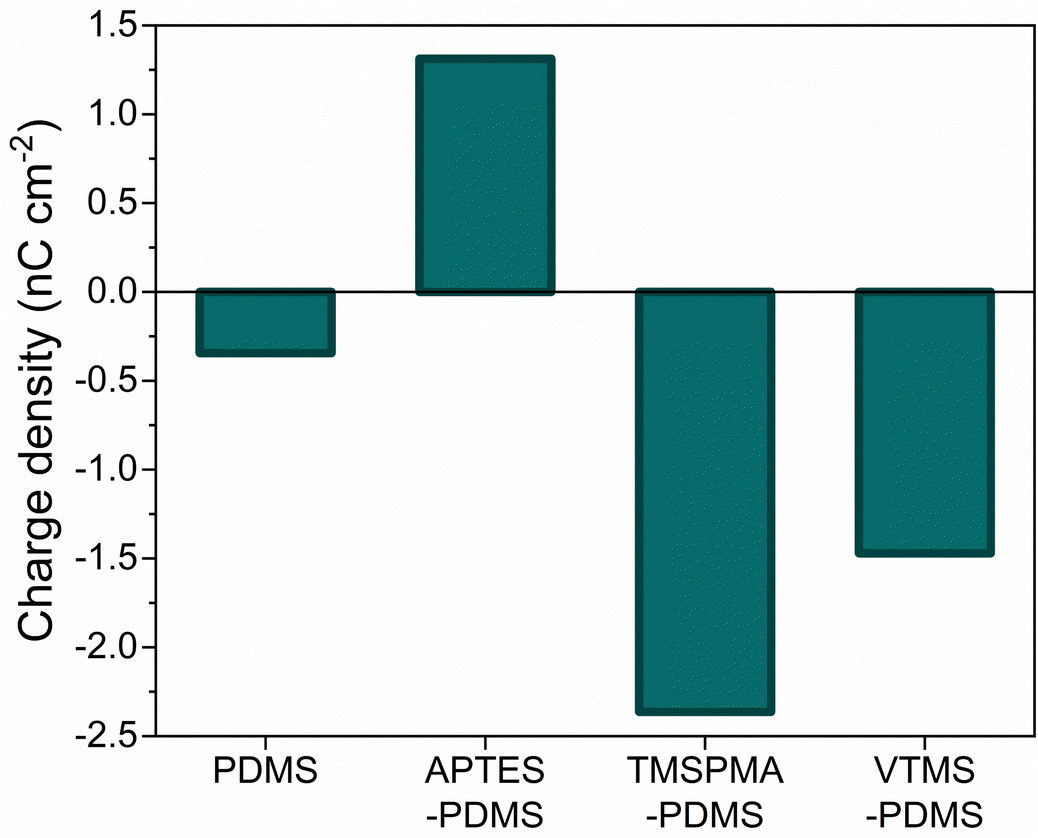 | ||
| Fig. 2 Surface charge density of PDMS and SAM-PDMS samples in contact-separation against an ITO electrode connected to an electrometer to measure current against ground. | ||
Contact-separation between two pristine PDMS with identical crosslinking degree results in a negligible charge density (0.001–0.002 nC cm−2).23,25 Since APTES-PDMS film shows a positive charge density but the highest negative charge was obtained for TMSPMA-PDMS film, this combination was chosen to assemble a TENG using SAM-PDMS as both contact layers. The assembled TENG demonstrated charge density of 1.16 nC cm−2 (Fig. 3A), VOC of 70 V and ISC of 700 nA (ESI† Fig. S8 and S9). The observed charge density is three orders of magnitude higher than that observed in contact-separation of two identical pristine PDMS layers. For comparison, TENGs were also assembled using different SAM-PDMS combinations. TENG using APTES-PDMS and VTMS-PDMS, which are also charged negatively, showed the charge density of only 0.49 nC cm−2. When a TENG was built using both samples that are charged negatively – VTMS-PDMS and TMSPMA-PDMS, the charge density was merely 0.29 nC cm−2.
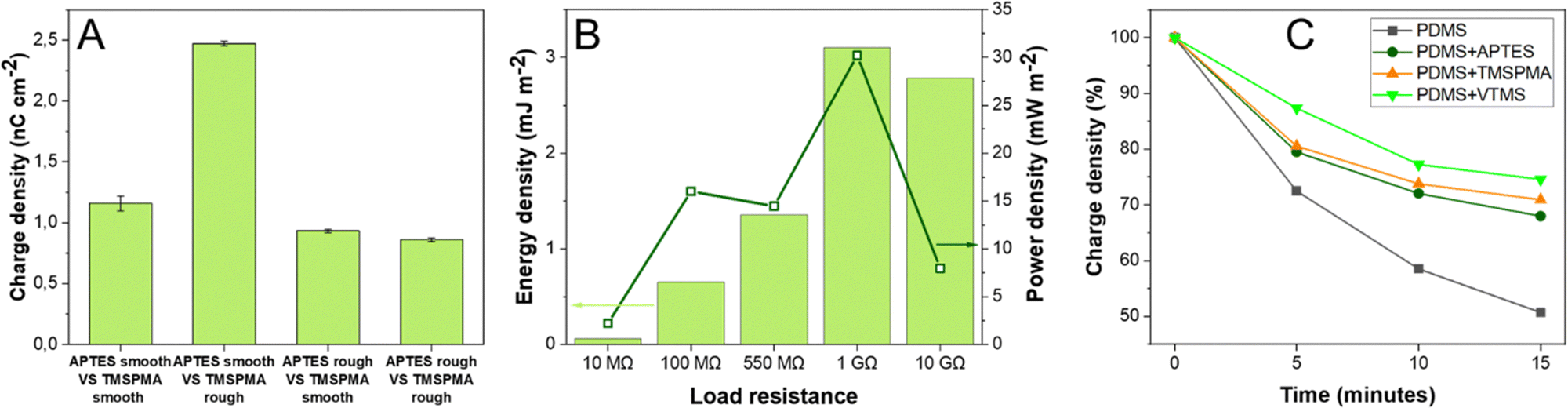 | ||
| Fig. 3 (A) Charge densities of TENGs based on APTES-PDMS and TMSPMA-PDMS films with various surface roughness. (B) Energy and power density of the TENG device based on smooth APTES-PDMS and rough TMSPMA-PDMS. (C) Current observed in contactless mode between pristine ITO and PDMS layers after 1000 contact-separation cycles. | ||
Charge density can be further increased by using rough and smooth surfaces as contact layers. SEM images of smooth and rough PDMS are shown in ESI† Fig. S10A and B, respectively. As shown in Fig. 2 the charge density after smooth PDMS was contact separated against ITO was 0.34 nC cm−2. Accordingly, the surface charge of rough PDMS was also determined in Faraday cup mode after contact-separation against ITO. The charge density reached −0.6 nC cm−2, which was more negative than in the case of smooth PDMS.
Next, both the smooth and rough films were functionalized by SAM. Since rough PDMS had shown relatively more negative charge, TMSPMA was introduced on the rough PDMS layer and accordingly for the smooth PDMS, with the less negative charge, the APTES SAM was used. Notably, a charge density of 2.50 nC cm−2 was obtained when smooth APTES-PDMS was contacted against rough TMSPMA-PDMS, as shown in Fig. 3A (corresponding current peaks are shown in ESI† Fig. S11–S13). Accordingly, when rough APTES-PDMS was contact-separated against smooth TMSPMA-PDMS almost 3 times lower charge density was registered (0.93 nC cm−2). This observation is in line with our previous results that contact-separation can be boosted by increasing the difference in surface roughness of both layers.45 Evidently, the direction of triboelectric dipole that forms between contact-separated layers is influenced both by the surface roughness and the type of SAM used for functionalization. These effects can be combined to obtain higher surface charge. In future studies this effect could be combined with other factors that influence the charge formation44 in contact-separation to achieve even greater triboelectric performance.
For the TENG assembled using smooth APTES-PDMS and rough TMSPMA-PDMS as contacting layers, the highest generated energy density of 3 mJ m−2 was observed at 1 GΩ load resistance (Fig. 3B green bars). 1 GΩ resistance was also the optimal load resistance for this TENG device since the highest power density of 31 mW m−2 was obtained from voltage measurements at this value (Fig. 3B dark green squares). For comparison, the TENG which was assembled using smooth APTES-PDMS and smooth TMSPMA-PDMS layers demonstrated the energy density of only 0.18 mJ m−2 at 1 GΩ and power density of 2.5 mW m−2 (ESI† Fig. S14). The observed energy and power densities suggest that the TENG device based on rough APTES-PDMS and smooth TMSPMA-PDMS layers with coordinated surface roughness values might be sufficient to power portable electronic devices. Since the TENG is assembled using PDMS/ITO as an electrode, the whole device is transparent, and for the TENG based on smooth APTES-PDMS and smooth TMSPMA-PDMS the visible light transmittance reaches 70% (ESI† Fig. S15). However, for the TENG based on smooth APTES-PDMS and rough TMSPMA-PDMS, the transmittance reaches only 25%. Nevertheless, transparency enables future application in optoelectronics or self-powered electronic displays and touchscreens.
Surface charge density is linked with the presence of mechanoradicals on the polymer surface and the formation of stable ion-radical pairs.46 Accordingly, an increase in the charge density generated during contact-separation for functionalized PDMS can be explained by the formation of relatively more stable ion-radical pairs. To test whether SAM-PDMS indeed possesses better charge stability, we performed non-contact oscillation of the charged films. Charge stability tests showed that for SAM-PDMS the decrease in charge density was lower than for non-functionalized PDMS. For non-functionalized PDMS after 15 min of oscillation the charge density decreased by 50% of the initial value (Fig. 3C). For SAM-PDMS layers the charge decrease in the same time period was much lower – APTES-PDMS decreased by 32%, TMSPMA-PDMS by 29% and VTMS-PDMS only by 25%.
Conclusions
In summary, the charge density generated in contact-separation of PDMS contact layers with identical crosslink degrees is increased by three orders of magnitude when one PDMS is functionalized by APTES and the other by TMSPMA. Charge density is further increased when contact-separating smooth and rough surfaces – the greatest charge density is seen for the combination of smooth APTES-PDMS and rough TMSPMA-PDMS. The obtained TENGs are transparent, thus opening pathways to incorporation in optoelectronic systems. Measurements in non-contact oscillation mode reveal that SAM-modified PDMS layers show higher charge density stability than pristine PDMS.Author contributions
L. Ģ. performed sample fabrication, surface functionalization and triboelectric measurements. L. L. performed ATR-FTIR measurements and charge stability tests. M. I. performed the XPS measurements. L. L. and A. Š conceived the idea. The manuscript was written through the contributions of all authors. All authors have given approval to the final version of the manuscript.Conflicts of interest
There are no conflicts of interest to declare.Acknowledgements
L. Ģ. acknowledges the financial support from the grant: “Strengthening the capacity of RTU scientific staff”, project No. ZM-2021/14.Notes and references
- L. Lapčinskis, K. Mālnieks, A. Linarts, J. Blūms, K. Šmits, M. Järvekülg, M. Knite and A. Šutka, ACS Appl. Energy Mater., 2019, 2, 4027 CrossRef.
- M. Kim, D. Park, M. M. Alam, P. Park and J. Nah, ACS Nano, 2019, 13, 4640 CrossRef CAS PubMed.
- J. Li, N. A. Shepelin, P. C. Sherell and A. V. Ellis, Chem. Mater., 2021, 33, 4304 CrossRef CAS.
- B.-Y. Lee, D. H. Kim, J. Park, K.-I. Park, K. J. Lee and C. K. Jeong, Sci. Technol. Adv. Mater., 2019, 20, 758 CrossRef CAS PubMed.
- G. Zhu, P. Bai, J. Chen and Z. L. Wang, Nano Energy, 2013, 2, 688 CrossRef CAS.
- I. Aazem, D. T. Mathew, S. Radhakrishnan, K. V. Vijoy, H. John, D. M. Mulvihill and S. C. Pillai, RSC Adv., 2022, 12, 10545 RSC.
- J. Zhong, Y. Zhang, Q. Zhong, Q. Hu, B. Hu, Z. L. Wang and J. Zhou, ACS Nano, 2014, 8, 6273 CrossRef CAS PubMed.
- Y. Wu, Y. Luo, T. J. Cuthbert, A. V. Shokurov, P. K. Chu, S.-P. Feng and C. Menon, Adv. Sci., 2022, 9, 2106008 CrossRef CAS PubMed.
- S. A. Lone, K. C. Lim, K. Kaswan, S. Chatterjee, K.-P. Fan, D. Choi, S. Lee, H. Zhang, J. Cheng and Z.-H. Lin, Nano Energy, 2022, 7, 107318 CrossRef.
- S. Zhang, C. Qu, Y. Xiao, H. Liu, G. Song and Y. Xu, Nanoscale, 2022, 14, 4244 RSC.
- Y. Song, W. Gao and H. Zhang, in Integrated Smart Micro-Systems Towards Personalized Healthcare, Wiley-VCH Verlag GmbH, Weinheim, 2022, Chapter 3, 77–99 Search PubMed.
- S. Wu, G. Li, W. Liu, D. Yu, G. Li, X. Liu, Z. Song, H. Wang and H. Liu, Nano Energy, 2022, 93, 106859 CrossRef CAS.
- B. Dudem, Y. H. Ko, J. W. Leem, S. H. Lee and J. S. Yu, ACS Appl. Mater. Interfaces, 2015, 7, 20520 CrossRef CAS PubMed.
- L. Zhang, B. Zhang, J. Chen, L. Jin, W. Deng, J. Tang, H. Zhang, H. Pan, M. Zhu, W. Yang and Z. L. Wang, Adv. Mater., 2016, 28, 1650 CrossRef CAS PubMed.
- Q. Sun, L. Wang, G. Ren, L. Zhang, H. Sheng, Y. Zhu, H. Wang, G. Lu, H.-D. Yu and W. Huang, Nano Energy, 2022, 92, 106840 CrossRef CAS.
- C.-R. Yang, C.-T. Ko, S.-F. Chang and M.-J. Huang, Nano Energy, 2022, 92, 106791 CrossRef CAS.
- Z. Chen, Y. Cao, W. Yang, L. An, H. Fan and Y. Guo, J. Mater. Chem. A, 2022, 10, 799 RSC.
- B. Chai, K. Shi, H. Zou, P. Jiang, Z. Wu and X. Huang, Nano Energy, 2022, 91, 106668 CrossRef CAS.
- G. Zu, Y. Wei, C. Sun and X. Yang, J. Mater. Chem., 2022, 57, 2813 CAS.
- S. Wang, Y. Zi, Y. S. Zhou, S. Li, F. Fan, L. Lin and Z. L. Wang, J. Mater. Chem. A, 2016, 4, 3728 RSC.
- J. Chen and Z. L. Wang, Joule, 2017, 1, 480 CrossRef CAS.
- A. Šutka, A. Linarts, K. Mālnieks, K. Stiprais and L. Lapčinskis, Mater. Horiz., 2020, 7, 520 RSC.
- A. Šutka, K. Mālnieks, L. Lapčinskis, P. Kaufelde, A. Linarts, A. Bērziņa, R. Zābels, V. Jurķāns, I. Gorņevs, J. Blūms and M. Knite, Energy Environ. Sci., 2019, 12, 2417 RSC.
- L. Lapčinskis, K. Mālnieks, J. Blūms, M. Knite, S. Oras, T. Käämbre, S. Vlassov, M. Antsov, M. Timusk and A. Šutka, Macromol. Mater. Eng., 2020, 305, 1900638 CrossRef.
- P. C. Sherrell, A. Sutka, N. A. Shepelin, L. Lapcinskis, O. Verners, L. Germane, M. Timusk, R. A. Fenati, K. Malnieks and A. V. Ellis, ACS Appl. Mater. Interfaces, 2021, 13, 44935 CrossRef CAS PubMed.
- H. Zou, Y. Zhang, L. Guo, P. Wang, X. He, G. Dai, H. Zheng, C. Chen, A. C. Wang, C. Xu and Z. L. Wang, Nat. Commun., 2019, 10, 1427 CrossRef PubMed.
- S. Li, Y. Fan, H. Chen, J. Nie, Y. Liang, X. Tao, J. Zhang, X. Chen, E. Fu and Z. L. Wang, Energy Environ. Sci., 2020, 13, 896 RSC.
- Y. Yang, H. Zhang, J. Chen, S. Lee, T.-C. Hou and Z.-L. Wang, Energy Environ. Sci., 2013, 6, 1744–1749 RSC.
- A. Ulman, Chem. Rev., 1996, 96, 1533 CrossRef CAS PubMed.
- Y.-H. Cheng, C.-J. Lee and C.-Y. Chang, Adv. Mater. Technol., 2021, 6, 2000985 CrossRef CAS.
- C. Chang and C. Wang, J. Mater. Chem. C, 2020, 8, 4542 RSC.
- G. Song, Y. Kim, S. Yu, M.-O. Kim, S.-H. Park, S. M. Cho, D. B. Velusamy, S. H. Cho, K. L. Kim, J. Kim, E. Kim and C. Park, Chem. Mater., 2015, 27, 4749 CrossRef CAS.
- S.-H. Shin, Y. E. Bae, H. K. Moon, J. Kim, S.-H. Choi, Y. Kim, H. J. Yoon, M. H. Lee and J. Nah, ACS Nano, 2017, 11, 6131 CrossRef CAS PubMed.
- S.-H. Shin, Y. H. Kwon, Y.-H. Kim, J.-Y. Jung, M. H. Lee and J. Nah, ACS Nano, 2015, 9, 4621 CrossRef CAS PubMed.
- R. Wolf and A. Sparavigna, Engineering, 2010, 2, 397 CrossRef CAS.
- M. Siek, W. Adamkiewicz, Y. I. Sobolev and B. A. Grzybowski, Angew. Chem., Int. Ed., 2018, 57, 15379 CrossRef CAS PubMed.
- S. Pan and Z. Zhang, Friction, 2019, 7, 2 CrossRef.
- A. Okbaz, A. Karabiber, A. Yar, Z. Kinas, A. Sarilmaz and F. Ozel, Energy Convers. Manage., 2022, 252, 115053 CrossRef CAS.
- R. Zhang, M. Hummelgård, J. Örtegren, M. Olsen, H. Andersson, Y. Yang, Z.-L. Wang, H. Olin, P. Sutar and D. Mihailovic, Nano Energy, 2021, 89, 106363 CrossRef CAS.
- L. Johnson, L. Gao, C. W. Shields IV, M. Smith, K. Efimenko, K. Cushing, J. Genzer and G. P. López, J. Nanobiotechnol., 2013, 11, 22 CrossRef CAS PubMed.
- T.-N. Le and C.-K. Lee, Appl. Biochem. Biotechnol., 2020, 191, 29 CrossRef CAS PubMed.
- V. Kumar, U. H. Ko, Y. Zhou, J. Hoque, G. Arya and S. Varghese, Adv. Intell. Syst., 2021, 3, 2100005 CrossRef.
- M. A. Sibeko and A. S. Luyt, Polym. Bull., 2014, 71, 637 CrossRef CAS.
- A. Šutka, K. Mālnieks, L. Lapčinskis, M. Timusk, K. Pudzs and M. Rutkis, iScience, 2020, 23, 101011 CrossRef PubMed.
- A. Šutka, K. Mālnieks, L. Lapčinskis, M. Timusk, K. Kalniņš, A. Kovaļovs, J. Bitenieks, M. Knite, D. Stevens and J. Grunlan, Phys. Chem. Chem. Phys., 2020, 22, 13299 RSC.
- T. Mazur and B. A. Gryzbowski, Chem. Sci., 2017, 8, 2025 RSC.
Footnote |
| † Electronic supplementary information (ESI) available. See DOI: https://doi.org/10.1039/d2ma01015a |
| This journal is © The Royal Society of Chemistry 2023 |