
 Open Access Article
 This Open Access Article is licensed under a Creative Commons Attribution-Non Commercial 3.0 Unported Licence
A C6-DPA/PMMA binary blend ink for high-performance inkjet-printed organic field-effect transistors†
Yang
Liu‡
a,
Chenhuai
Yang‡
a,
Ting
Jiang
b,
Yuanrong
Bao
a,
Lu
Wang
a,
Deyang
Ji
 *b,
Fangxu
Yang
a,
Fei
Jiao
*a and
Wenping
Hu
ac
*b,
Fangxu
Yang
a,
Fei
Jiao
*a and
Wenping
Hu
ac
aTianjin Key Laboratory of Molecular Optoelectronic Sciences, Department of Chemistry, School of Science, Tianjin University, Tianjin 300072, China. E-mail: feijiao@tju.edu.cn
bInstitute of Molecular Aggregation Science of Tianjin University, Tianjin 300072, China. E-mail: jideyang@tju.edu.cn
cHaihe Laboratory of Sustainable Chemical Transformations, Tianjin 300192, China
First published on 22nd November 2022
Abstract
A solution-processed small-molecule/insulator binary blend offers an optimized blending system for inkjet-printing technology. Due to the spontaneous vertical phase separation, a small-molecule OSC thin-film could be deposited with good crystallization and preferred orientation. However, the uniformity of the semiconducting thin-film is still a critical issue, and the intrinsic properties of the blend ink used in inkjet printing, especially ink stability, are rarely reported. In this paper, a blend system of 2,6-bis(4-hexylphenyl)anthracene (C6-DPA) and polymethyl methacrylate (PMMA) is used to prepare a high-performance and stabilized electronic ink. Based on this ink, the highest mobility of inkjet-printed organic field-effect transistors is up to 2.01 cm2 V−1 s−1 with bottom-gate and top-contact structures.
Introduction
Printed organic field-effect transistors (OFETs) have been extensively investigated because of their low-cost and large-area printing process, mechanical flexibility, and compatibility with industrial production.1–4 Among different printing technologies, inkjet-printing is attractive because the ink can be deposited on demand directly onto any substrate without a mask or additional etching processes.5–8 Small-molecule organic semiconductors (OSCs) are popular active materials in inkjet-printed OFETs due to their high mobility and good solubility in organic solvents.9–12 However, the formation of continuous small-molecule OSC films via inkjet printing is challenging due to the molecular shape, packing anisotropies and ink dewetting.13 Blending small-molecule OSCs with insulating polymers has been demonstrated as an effective route for improving the film uniformity and performance of OFETs.14–17 Vertical phase separation occurs spontaneously in the blend due to Marangoni-like instability during solvent evaporation. Semiconductors typically enrich at the upper or lower interface of the film and facilitate the formation of a uniform and continuous crystalline film, which provides an effective way for charge transport.18 The use of a small-molecule OSC/polymer blend system to prepare inkjet-printed OFETs has also been investigated.19–22 Cho et al. reported the vertical phase-separation in an inkjet-printed 6,13-bis(triisopropylsilylethynyl)pentacene (TIPS-PEN)/amorphous polycarbonate (APC) blend film, where the improvement in the hole mobilities of OFETs was attributed to the movement of the TIPS-PEN molecules toward the air/film interface.19 Jiang et al. optimized the performance of inkjet-printed OFETs and constructed a high-gain, fully inkjet-printed Schottky barrier organic thin-film transistor amplifier circuit by adopting a dioctylbenzothienobenzothiophene(C8-BTBT)/PMMA blend. The transistor signal amplification efficiency was 38.2 S A−1 with an ultralow power consumption of <1 nW.22 Although high performance of the above OFET devices is realized, the uniformity of the OSC thin film is still a critical issue, mainly due to the homogeneous nucleation of the small-molecule OSCs on the substrate.23–26Here, we report a stabilized organic semiconducting electronic ink for inkjet-printed high-performance OFETs. The small-molecule semiconductor 2,6-bis(4-hexylphenyl) anthracene (C6-DPA) is chosen due to its high mobility, high solubility in various organic solvents, commercial availability, as well as good air stability.27–35 And polymethyl methacrylate (PMMA) is chosen for our binary blend ink system because of its excellent chemical stability, mechanical properties, easy processing ability and transparency.29,36,37 We begin by systematically investigating the effect of solvents, ink concentrations and different blend ratios on the ink stability and microstructure of printed thin films. The structural and electrical properties of the blend films in OFETs are further studied. The maximum field-effect mobility of 2.01 cm2 V−1 s−1 is obtained when the ink was under its optimal conditions, which is comparable to the values reported in single crystal devices.
Results and discussion
For drop-on-demand (DOD) inkjet printing, the rheological properties of the ink, especially the surface tension (γ) and viscosity (η), must be strictly controlled to make sure that the ink can be printed accurately.38–40 The ink printability can be described using the inverse Ohnesorge (Oh) number (Z), which is defined as: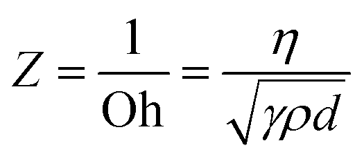 | (1) |
![[thin space (1/6-em)]](https://www.rsc.org/images/entities/char_2009.gif) 000 is selected due to its large molecular weight to provide sufficient vertical phase separation and suitable viscosity.27 By calculating the Z value, the optimal ratio of the blend system is further determined. As recorded in Table S2 (ESI†), the optimal ratio range of the C6-DPA ink for inkjet printing should be less than 75 wt%.
000 is selected due to its large molecular weight to provide sufficient vertical phase separation and suitable viscosity.27 By calculating the Z value, the optimal ratio of the blend system is further determined. As recorded in Table S2 (ESI†), the optimal ratio range of the C6-DPA ink for inkjet printing should be less than 75 wt%.
 | ||
| Fig. 1 (a) Surface tension of the ink with different solvents or concentrations. The surface tension of the ink is basically independent of its concentration, but closely related to the type of pure solvent. (b) Ink viscosity with different molecular masses of PMMA or concentrations. (c) Surface tension and viscosity of the ink with different blend ratios. Here, the ink concentration is 4 mg mL−1, TCB is used as a solvent, and the molecular weight of PMMA is 550000. | ||
In order to further confirm the optimal ink conditions and obtain the optimal thin film morphology for OFET devices, we prepared the blend inks under different conditions. Polarized optical microscopy (POM) images showed a strong dependence of the film morphology on the solvents, the ink concentration, and blend ratio (Fig. S2, ESI†). As a result, highly crystalline films can be prepared in blended inks with TCB as the solvent and an ink concentration of 4 mg mL−1. When the microstructure of the film was investigated by atomic force microscopy, it was noticed that when the mixing ratio of C6-DPA/PMMA was 2:1, the morphology of the film was more uniform, and the root mean square roughness was only 0.948 nm (Fig. 2a–d and Fig. S3, ESI†). These results show that the vertical phase separation of the films is the best at this mixing ratio. For small molecule and polymer blend systems, during the solvent evaporation process, due to the different adhesion of dissolved components to the substrate, the interaction between the solute and the substrate induces vertical phase separation, and compounds with higher surface energy tend to be preferentially cured on the substrate surface.22,42,43 In the mixed ink system, there is a more favourable enthalpy interaction between PMMA and SiO2,42 thus PMMA will preferentially deposit on the SiO2 substrate, while the more hydrophobic C6-DPA small molecules will crystallize at the interface of air and the film, which is confirmed in the cross-sectional scanning electron microscope (SEM) image (Fig. 2h and Fig. S4, ESI†). When the proportion of PMMA increases, the small molecule OSCs cannot be separated from the polymer, instead they form dispersed crystal domains. This deteriorating degree of vertical phase separation can be reflected from the film roughness increase of the corresponding AFM images. This conclusion was confirmed by X-ray diffraction (XRD) measurements, as shown in Fig. S5 (ESI†). The diffraction peaks at 2θ = 2.7° of the films with other different blending ratios are weak, while the diffraction peaks of the films using C6-DPA/PMMA (2:1) are sharper and stronger, indicating that the C6-DPA films have higher crystallinity. Furthermore, the diffraction peak intensities of the films are positively correlated with the molecular weight of the PMMA used, which is consistent with previous reports.44 Fig. S6 (ESI†) shows the optical microscopy (OM) images of an inkjet-printed droplet array of the blend ink, and the diameter of each droplet is about 50–60 μm with the optimal printing spacing D of 1/2–2/3 of the diameter of each droplet. When the spacing of droplets is set to 25 μm, a printed line with better shape is obtained. Furthermore, inkjet-printed C6-DPA films can also be fabricated (Fig. 2e). The two halves of the film exhibited simultaneous extinction with a 45° rotation of the polarization angle (Fig. 2f and g), suggesting that specific regions of the pattern may be single-crystal domains. Therefore, the optimal state of the ink is TCB as the solvent, with an ink concentration of 4 mg mL−1, and a C6-DPA/PMMA mass ratio of 2:1. It is worth mentioning that although the ink can form thin films when the concentration of C6-DPA is larger than 3 mg mL−1, the solute will precipitate out after the ink is left at room temperature for several days.
 | ||
| Fig. 2 (a–d) AFM images of the ink-printed C6-DPA film based on 4:1, 3:1, 2:1 and 1:1 C6-DPA/PMMA ratios. (e) OM and (f and g) POM images of the inkjet-printed crystalline film based on a 2:1 C6-DPA/PMMA ratio. The crossed arrows indicate the orientation of crossed polarizers. (h) Cross-sectional SEM image of a blend film with a 2:1 mix ratio. | ||
To study the electrical properties of inks at different blend ratios, the electrical characteristics of C6-DPA films with different blend proportions were studied by constructing OFETs with a bottom-gate top-contact configuration using inkjet printing. Compared with the Ag electrode, the work function of the Au electrode is more matched with the energy level of C6-DPA.27,30 However, the deposition of the gold electrode will cause more serious thermal damage to our thin film, so we chose the Ag electrode. 300 nm SiO2 was used as the dielectric layer and 40 nm Ag was adopted as the source and drain electrodes by thermal evaporation. The source–drain electrodes were smaller than the pattern size (Fig. 3a), which allows the measurement of the local C6-DPA film properties to test the uniformity of the C6-DPA film and obtain the spatial information of the electrical properties.45 Because the underlying polymer is thin enough, calculated field-effect mobilities in this work only consider the capacitance of the SiO2 dielectric regardless of the capacitance of PMMA, which results in a slight underestimation of the mobilities for all OFETs in this work. Before the I–V measurement, the thin film was divided into individual areas by probe tips scratching along the electrodes to avoid the fringe effect. The field-effect mobility of OFETs at the saturation region was calculated from the transfer I–V curves.
 | ||
| Fig. 3 (a) The schematic diagram of the device preparation process, the chemical structure of blend inks and the test structure of the OFETs. (b) Transfer characteristics measured for bottom-gate, top-contact transistors with different blend ratios of C6-DPA/PMMA (ink concentration is 4 mg mL−1). (c) Output characteristics of OFETs prepared when the blend ratio of C6-DPA/PMMA is 2:1. (d) Comparison of mobility of OFETs based on C6-DPA. (e) An OM image of the printed 4 × 4 C6-DPA thin film transistor array. (f) The distribution and (g) histogram of saturation mobility of 16 OFETs from the corresponding 4 × 4 array. | ||
We plotted the transfer I–V curves and extracted mobilities (Fig. 3b and Fig. S7, ESI†) of C6-DPA/PMMA blends at different blend ratios (ink concentration = 4 mg mL−1) to find the optimal value, where the average mobility was obtained based on 16 OFET measurements for each condition. The plot showed that the highest hole mobility was achieved when the blend ratio of C6-DPA/PMMA was equal to 2:1. The device performance obviously decreased when the blend ratio was less than 2:1, which may be because the amount of C6-DPA cannot completely cover the whole film and due to the appearance of dendrites and cracks in the C6-DPA film. The hole mobility also decreased when the blend ratio exceeded 2:1, in which small-molecules became stranded in the polymer due to the low concentration of the polymer, preventing the small-molecule OSCs from moving to the upper layer and deteriorating the effect of vertical phase separation. As a result, the highest OFET performance was achieved at 4 mg mL−1 with a 2:1 blend ratio (C6-DPA = 2.65 mg mL−1, PMMA = 1.35 mg mL−1), the on/off ratio was greater than 107 and the maximum hole mobility was approximately 2.01 cm2 V−1 s−1 in the saturation regime, outperforming the vast majority of C6-DPA-based single-crystal transistors (Fig. 3d). Then we selected a 4 × 4 transistor array (Fig. 3e), and counted its mobility distribution as shown in Fig. 3f and g. The mobility distribution is uniform, indicating that the uniformity between devices has been greatly improved, laying a solid foundation for its industrial application.
More importantly, the C6-DPA/PMMA binary blend ink remained transparent, uniform and stable in air for two months, as shown in Fig. 4a. Encouragingly, the performance of devices fabricated based on the ink stored for two months did not degrade significantly, indicating good air stability of the blend ink.
 | ||
| Fig. 4 (a) The electronic inks with different blend ratios of C6-DPA/PMMA. (b) Transfer curves of OFETs based on electronic inks stored for different times. | ||
Conclusions
In conclusion, we prepared a functional C6-DPA/PMMA binary blend ink with high environmental stability and good performance. By introducing the insulating polymers and careful control of the vertical phase separation of the C6-DPA/PMMA binary blend ink, the crystallization of the C6-DPA film and device-to-device uniformity were improved distinctly. Through the analysis and characterization of inks with different conditions, we obtained the best ink preparation conditions, and the stability of the ink was guaranteed. Finally, we prepared highly stable and high-performance OFET devices through inkjet printing technology. This provides research guidance and the direction for the functionalization and commercialization of organic semiconductor inks.Conflicts of interest
There are no conflicts to declare.Acknowledgements
The authors are grateful for the financial support from the National Key Research and Development Program (2021YFB3600700), the National Natural Science Foundation of China (52121002) and the Haihe Laboratory of Sustainable Chemical Transformations.References
- C. D. Dimitrakopoulos and P. R. L. Malenfant, Adv. Mater., 2002, 14, 99 CrossRef CAS.
- F. Yang, L. Sun, Q. Duan, H. Dong, Z. Jing, Y. Yang, R. Li, X. Zhang, W. Hu and L. Chua, SmartMat, 2021, 2, 99 CrossRef CAS.
- S. R. Forrest, Nature, 2004, 428, 911 CrossRef.
- M. Baklar, P. H. Wobkenberg, D. Sparrowe, M. Goncalves, I. McCulloch, M. Heeney, T. Anthopoulos and N. Stingelin, J. Mater. Chem., 2010, 20, 1927 RSC.
- F. Garnier, R. Hadjaoui, A. Yasser and P. Srivastava, Science, 1994, 265, 1684 CrossRef PubMed.
- H. Sirringhaus, T. Kawase, R. H. Friend, T. Shimoda, M. Inbasekaran, W. Wu and E. P. Woo, Science, 2000, 290, 2123 CrossRef.
- R. A. Street, W. S. Wong, S. E. Ready, I. L. Chabinyc, A. C. Arias, S. Limb, A. Salleo and R. Lujan, Mater. Today, 2006, 9, 32 CrossRef.
- H. E. Katz, Chem. Mater., 2004, 16, 4748 CrossRef CAS.
- D. Kwak, H. H. Choi, B. Kang, D. H. Kim, W. H. Lee and K. Cho, Adv. Funct. Mater., 2016, 26, 3003 CrossRef CAS.
- K. Zhao, O. Wodo, D. Ren, H. U. Khan, M. R. Niazi, H. Hu, M. Abdelsamie, R. Li, E. Q. Li and L. Yu, Adv. Funct. Mater., 2016, 26, 1737 CrossRef CAS.
- A. F. Paterson, N. D. Treat, W. Zhang, Z. Fei, G. Wyatt-Moon, H. Faber, G. Vourlias, P. A. Patsalas, O. Solomeshch, N. Tessler, M. Heeney and T. D. Anthopoulos, Adv. Mater., 2016, 28, 7791 CrossRef CAS PubMed.
- H. Minemawari, T. Yamada, H. Matsui, J. Tsutsumi, S. Haas, R. Chiba, R. Kumai and T. Hasegawa, Nature, 2011, 475, 364 CrossRef CAS.
- J. Kang, N. Shin, D. Y. Jang, V. M. Prabhu and D. Y. Yoon, J. Am. Chem. Soc., 2008, 130, 12273 CrossRef CAS PubMed.
- Y. S. Chung, N. Shin, J. Kang, Y. Jo, V. M. Prabhu, S. K. Satija, R. J. Kline, D. M. DeLongchamp, M. F. Toney, M. A. Loth, B. Purushothaman, J. E. Anthony and D. Y. Yoon, J. Am. Chem. Soc., 2011, 133, 412 CrossRef CAS.
- C. Reese and Z. Bao, Mater. Today, 2007, 10, 20 CrossRef CAS.
- M. S. Ozório, G. L. Nogueira, R. M. Morais, C. S. Martin, C. J. L. Constantino and N. Alves, Thin Solid Films, 2016, 608, 97 CrossRef.
- K. Zhao, O. Wodo, D. Ren, H. U. Khan, M. R. Niazi, H. Hu, M. Abdelsamie, R. Li, E. Li and L. Yu, Adv. Funct. Mater., 2016, 26, 1737 CrossRef CAS.
- T. Ohe, M. Kuribayashi, R. Yasuda, A. Tsuboi, K. Nomoto, K. Satori, M. Itabashi and J. Kasahara, Appl. Phys. Lett., 2008, 93, 053303 CrossRef.
- J. Smith, R. Hamilton, M. Heeney, D. M. de Leeuw, E. Cantatore, J. E. Anthony, I. McCulloch, D. D. C. Bradley and T. D. Anthopoulos, Appl. Phys. Lett., 2008, 93, 253301 CrossRef.
- Y. Li, C. Liu, M. V. Lee, Y. Xu, X. Wang, Y. Shi and K. Tsukagoshi, J. Mater. Chem. C, 2013, 1, 1352 RSC.
- W. Lee and Y. Park, Polymers, 2014, 6, 1057 CrossRef.
- S. Y. Cho, J. M. Ko, J. Lim, J. Y. Lee and C. Lee, J. Mater. Chem. C, 2013, 1, 914 RSC.
- M. B. Madec, P. J. Smith, A. Malandraki, N. Wang, J. G. Korvink and S. G. Yeates, J. Mater. Chem., 2010, 20, 9155 RSC.
- C. Jiang, H. W. Choi, X. Cheng, H. Ma, D. Hasko and A. Nathan, Science, 2019, 363, 719 CrossRef CAS PubMed.
- L. Feng, C. Jiang, H. Ma, X. Guo and A. Nathan, Org. Electron., 2016, 38, 186 CrossRef CAS.
- Z. Zhou, Q. Wu, S. Wang, Y. Huang, H. Guo, S. Feng and P. K. L. Chan, Adv. Sci., 2019, 6, 1900775 CrossRef CAS PubMed.
- C. Xu, P. He, J. Liu, A. Cui, H. Dong, Y. Zhen, W. Chen and W. Hu, Angew. Chem., Int. Ed., 2016, 55, 9519 CrossRef.
- Q. Wang, F. Yang, Y. Zhang, M. Chen, X. Zhang, S. Lei, R. Li and W. Hu, J. Am. Chem. Soc., 2018, 140, 5339 CrossRef PubMed.
- X. Zhu, Q. Wang, X. Tian, X. Zhang, Y. Feng, W. Feng, R. Li and W. Hu, J. Mater. Chem. C, 2018, 6, 12479 RSC.
- S. Duan, X. Gao, Y. Wang, F. Yang, M. Chen, X. Zhang, X. Ren and W. Hu, Adv. Mater., 2019, 31, 1807975 CrossRef.
- X. Zhu, Y. Zhang, X. Ren, J. Yao, S. Guo, L. Zhang, D. Wang, G. Wang, X. Zhang, R. Li and W. Hu, Small, 2019, 15, 1902187 CrossRef PubMed.
- J. Yao, Y. Zhang, X. Tian, X. Zhang, H. Zhao, X. Zhang, J. Jie, X. Wang, R. Li and W. Hu, Angew. Chem., Int. Ed., 2019, 58, 16082 CrossRef.
- Z. Chen, S. Duan, X. Zhang, B. Geng, Y. Xiao, J. Jie, H. Dong, L. Li and W. Hu, Adv. Mater., 2021, 2104166 Search PubMed.
- J. Yao, X. Tian, S. Yang, F. Yang, R. Li and W. Hu, APL Mater., 2021, 9, 051108 CrossRef.
- X. Tian, J. Yao, S. Guo, Z. Wang, Y. Xiao, H. Zhang, Y. Feng, W. Feng, J. Jie, F. Yang, R. Li and W. Hu, J. Mater. Chem. C, 2022, 10, 2575 RSC.
- S. Chung, K. Cho and T. Lee, Adv. Sci., 2019, 6, 1801445 CrossRef PubMed.
- G. Mattana, A. Loi, M. Woytasik, M. Barbaro, V. Noël and B. Piro, Adv. Mater. Technol., 2017, 2, 1700063 CrossRef.
- S. J. Lee, Y.-J. Kim, S. Y. Yeo, E. Lee, H. S. Lim, M. Kim, Y.-W. Song, J. Cho and J. A. Lim, Sci. Rep., 2015, 5, 14010 CrossRef.
- C. Xu, P. He, J. Liu, A. Cui, H. Dong, Y. Zhen, W. Chen and W. Hu, Angew. Chem., Int. Ed., 2016, 55, 9519 CrossRef.
- M. R. Niazi, R. Li, E. Qiang Li, A. R. Kirmani, M. Abdelsamie, Q. Wang, W. Pan, M. M. Payne, J. E. Anthony, D.-M. Smilgies, S. T. Thoroddsen, E. P. Giannelis and A. Amassian, Nat. Commun., 2015, 6, 8598 CrossRef.
- A. Hamaguchi, T. Negishi, Y. Kimura, Y. Ikeda, K. Takimiya, S. Z. Bisri, Y. Iwasa and T. Shiro, Adv. Mater., 2015, 27, 6606 CrossRef PubMed.
- Q. Wang, F. Yang, Y. Zhang, M. Chen, X. Zhang, S. Lei, R. Li and W. Hu, J. Am. Chem. Soc., 2018, 140, 5339 CrossRef CAS.
- Y. Zhou, O. S. Game, S. Pang and N. P. Padture, J. Phys. Chem. Lett., 2015, 6, 4827 CrossRef CAS PubMed.
- J. A. Lim, W. H. Lee, H. S. Lee, J. H. Lee, Y. D. Park and K. Cho, Adv. Funct. Mater., 2008, 18, 229 CrossRef CAS.
- A. Pierre, M. Sadeghi, M. M. Payne, A. Facchetti, J. E. Anthony and A. C. Arias, Adv. Mater., 2014, 26, 5722 CrossRef CAS.
Footnotes |
| † Electronic supplementary information (ESI) available. See DOI: https://doi.org/10.1039/d2ma00993e |
| ‡ These authors made an equal contribution to this work |
| This journal is © The Royal Society of Chemistry 2023 |