
 Open Access Article
 This Open Access Article is licensed under a Creative Commons Attribution-Non Commercial 3.0 Unported Licence
In situ transmission electron microscopy as a toolbox for the emerging science of nanometallurgy
Diego S. R.
Coradini
 *a,
Matheus A.
Tunes
b,
Patrick
Willenshofer
a,
Sebastian
Samberger
a,
Thomas
Kremmer
a,
Phillip
Dumitraschkewitz
a,
Peter J.
Uggowitzer
a and
Stefan
Pogatscher
a
*a,
Matheus A.
Tunes
b,
Patrick
Willenshofer
a,
Sebastian
Samberger
a,
Thomas
Kremmer
a,
Phillip
Dumitraschkewitz
a,
Peter J.
Uggowitzer
a and
Stefan
Pogatscher
a
aChair of Non-Ferrous Metallurgy, Montanunversitaet Leoben, Austria. E-mail: nemetall@unileoben.ac.at
bMaterials Science and Technology Division, Los Alamos National Laboratory, USA. E-mail: tunes@lanl.gov
First published on 16th June 2023
Abstract
Potential applications of nanomaterials range from electronics to environmental technology, thus a better understanding of their manufacturing and manipulation is of paramount importance. The present study demonstrates a methodology for the use of metallic nanomaterials as reactants to examine nanoalloying in situ within a transmission electron microscope. The method is further utilised as a starting point of a metallurgical toolbox, e.g. to study subsequent alloying of materials by using a nanoscale-sized chemical reactor for nanometallurgy. Cu nanowires and Au nanoparticles are used for alloying with pure Al, which served as the matrix material in the form of electron transparent lamellae. The results showed that both the Au and Cu nanomaterials alloyed when Al was melted in the transmission electron microscope. However, the eutectic reaction was more pronounced in the Al–Cu system, as predicted from the phase diagram. Interestingly, the mixing of the alloying agents occurred independently of the presence of an oxide layer surrounding the nanowires, nanoparticles, or the Al lamellae while performing the experiments. Overall, these results suggest that transmission electron microscope-based in situ melting and alloying is a valuable lab-on-a-chip technique to study the metallurgical processing of nanomaterials for the future development of advanced nanostructured materials.
Introduction
Energy efficiency and the generation of green energy are trending topics affecting technological development and the design of new materials. To ensure continued economic progress, today's technologies are often based on nanotechnology, which aims at improving both properties and efficiency of existing functional materials. New applications need to comply with stricter environmental and climate protection policies.1 There are many examples of novel nanomaterial applications varying from electronics to environmental engineering where the manipulation on chips at nanoscale is of great research and development interest.1–4 For instance, in the electronics industry, the most commonly discussed challenges concern the miniaturization of circuitry and an increase in efficiency.1,5,6 In the energy storage branch nanometallic alloys are being studied as possible candidates capable of storing thermal energy.7 In medicine, nanomaterials can be used as drug-delivery systems and biosensors.8 Environmental engineering uses nanofilters for water cleaning and waste recycling. In the case of polymers, nanoadditives can be added within the process to improve the properties of the recycled material.9 Other important applications comprise the use of nanoadditives to depolymerize polymers back to monomers for recycling10 and nanostructuring materials via additive manufacturing which can positively affect the final product properties.11 Nevertheless, complex manufacturing methods are necessary to enable such applications. Production-wise, two different classifications are considered: top-down and bottom-up processes. The top-down process focuses on atomizing a bulk precursor, which can agglomerate in a film.12 On the other hand, bottom-up aims at producing material by using basic fundamental blocks like atoms or molecules to generate its final product.13–16 As a general example of the top-down route, one could refer to nanolithography,15,17 where the material is etched from bulk to the desired volume. For the bottom-up route, one can consider techniques like chemical-vapor deposition (CVD), and plasma or flame spraying synthesis.18,19Considering traditional smelting metallurgy on the nanoscale, current literature is limited. Many manufacturing methodologies of nanoscaled materials are based on the bottom-up route. For instance, metallic nanoparticles can be produced via organometallic synthesis or by using a colloidal solution.20 An alternative could be to use laser metallurgy for the manufacturing of nanoparticles.21 For the production of alloy nanoclusters (nanoalloys) ultrasonication can be employed, as it is used in the case of Bi–Sn eutectic nanoalloys.22 Besides, other techniques like laser vaporization, radiolysis, electrochemical synthesis, ion implantation, chemical reduction, and ion sputtering can be applied in the production of nanoalloys.23 Ultimately, upon demonstration of alloy design, manufacturing and manipulation at the nanoscale (i.e. nanometallurgy), a long-standing desire24 of producing light sails for photonic-based propulsion of interstellar probes up to fractions of the speed-of-light could be realized and nanomaterials have been recently investigated in this context.25,26
The current study aims to introduce a new nanometallurgical method for exploring alloying and phase transformations using nanomaterials in transmission electron microscopy (TEM). This lab-on-a-chip approach, which uses the TEM as a chemical reactor for metals, is based on a previously described method by Tunes et al.27 where a material can be deposited on a micro-electro-mechanical systems (MEMS) chip without the need for focused ion beam (FIB) preparation. The experiments focus on the Al–Cu and Al–Au systems since both have well-established literature on their thermodynamic properties and precipitation sequences.28–31 In addition, Cu is a common alloying agent in commercial Al-based systems used for improving precipitation hardening.32–34 Therefore, to validate the methodology, the results obtained are compared with previous findings available in the literature.
Methods
TEM sample preparation
The methodology used for the in situ nanomelting and heat treatment setup is shown in Fig. 1. The drawing illustrates the sequence of steps necessary to obtain a viable sample. The first step is based on the methodology presented by Tunes et al.,27 in which a jet-electropolished electron-transparent sample can be sectioned and transferred onto a MEMS chip. For later alloying, a nanomaterial-diluted solution is pipetted upon the latter, which is the substrate and will act as a matrix material. Nanoparticles (NPs) or nanowires (NWs) can also be added before the substrate is transferred to the MEMS chips.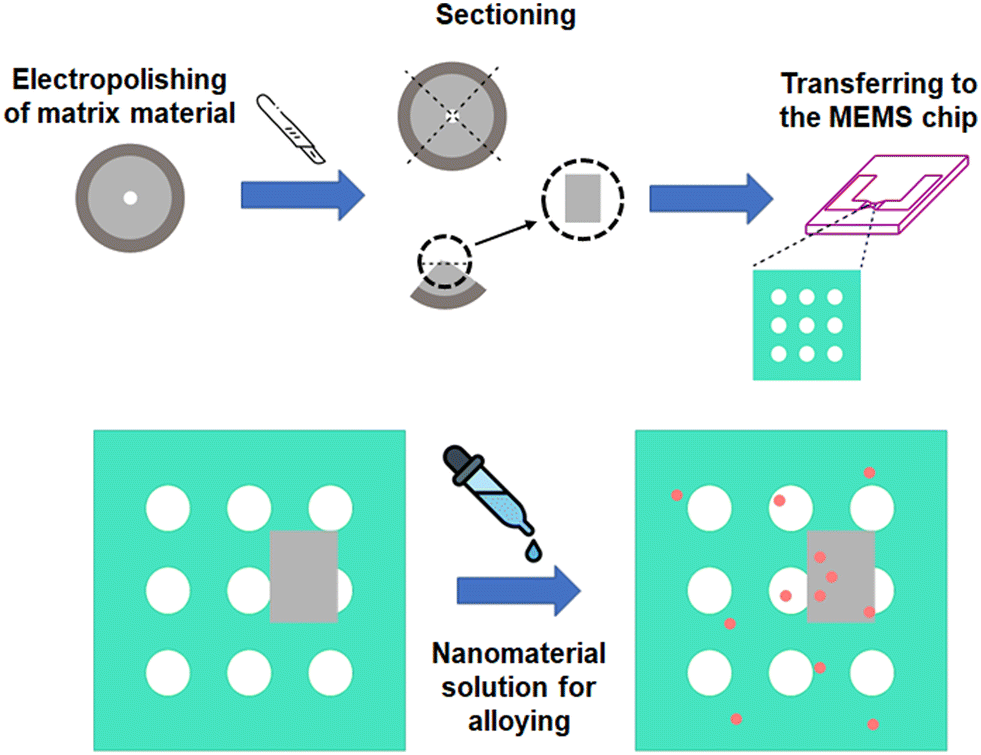 | ||
| Fig. 1 The sketch illustrates the preparation of the sample prior to the heating experiments. The sample is electropolished, sectioned using a scalpel, and transferred to a chip where NW or NP solutions are added. Note: this methodology is a modified, but new version of a previously reported sample preparation method for MEMS/TEM analysis.27 | ||
The material used as substrate and base for the in situ alloying was pure Al supplied by Sigma-Aldrich with 99.999% purity. For electropolishing, a Struers TenuPol-5 twin-jet electropolishing system was used. The temperature used was −25 °C, the voltage was set to 12 V, and the electropolishing solution was composed of 33% nitric acid and 66% methanol in vol%. After the electropolishing, the TEM lamella was sectioned using a ZEISS Stereo Discovery V12 light stereo-microscope. The sample was divided into 4 equal pieces, where the scalpel cuts through the sample taking the middle as the hole formed by the electropolishing. After the first sectioning, the exposed electron-transparent area is cut again until a piece around 50 μm in diameter is obtained. The sample is then transferred to the MEMS chip sensor membrane with the help of a fine electrostatic bristle used as a manipulator.27 SiN-coated e-chips from Protochips for vacuum applications were used as MEMS chips. Two solutions supplied by Sigma-Aldrich, one containing Cu nanowires, serial number MKCL4540, and the other containing Au nanoparticles, serial number MKCK9621, were used as the carrier substance to be used as alloying elements. The initial solution contained 5 mg Cu NWs (99.999%) in 1 ml of ethyl alcohol with an average diameter of 80 ± 60 nm. The Au NPs were supplied in powder condition with sizes smaller than 100 nm and a purity level of 99.9%. To avoid stacking the NWs and NPs on the MEMS e-chips, the solution was diluted to 0.126 wt% for both, the Cu-NWs and the Au-NPs. Prior to TEM pre-characterization, the diluted solutions were treated in an ultrasonic bath for 15 min to further disperse the particles in solution. After treatment in the ultrasonic bath, 3 drops of 20 μm of the solution were poured onto the MEMS chips. This step was repeated once the first application was dried. The specimen was then adjusted with help of the bristle, and the e-chip was then placed on the Fusion Select double-tilt holder from Protochips.35
MEMS chip sensor calibration
The MEMS chips used in the experiments were additionally calibrated for increased temperature accuracy in the applied temperature ramps. The calibration was performed using a pure Al sample before adding the nanoparticle solution. The FUSION software was utilized to create a heating program that would heat the Al until melting was observed, with the temperature at which melting occurred being considered 660 °C. The melting was confirmed by a decrease in the volume of the specimen, as demonstrated in Fig. 2. The change in shape was used as a marker for melting, as molten material tends to spheroidize. To prevent excessive spheroidization during the following experiments, the material was kept at the melting temperature for only 300 ms.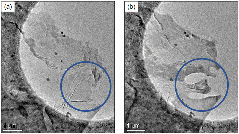 | ||
| Fig. 2 BFTEM micrographs featuring an Al thin foil resting on a SiN substrate. The Al foil appears as a translucent, ghostly veil against the darker gray of the substrate. The brighter area on the image indicates a hole present on the SiN substrate. In (a) and (b), a change in shape can be observed within the region highlighted by a blue circle. This alteration in shape was the result of melting and served as a temperature calibration. | ||
Heating programs and characterization
The heating programs were designed to allow a meaningful characterization of the sample. Moreover, a comparison of the sample was done prior to and after each step by using a selected area electron diffraction (SAED) pattern, and energy dispersive X-ray spectroscopy (EDX). Further, bright-field TEM and HAADF micrographs were taken. The heating programs used, varied accordingly to the system in question (Al–Au, and Al–Cu), and quenching was done after each heating step to preserve the microstructural state developed during the heat treatment.The two binary systems, Al–Cu and Al–Au, have in common that an eutectic is present on the Al-rich side, Al–Al2Cu and Al–Al2Au, respectively. The eutectic temperature is 548 °C for Al–Al2Cu and 650 °C for Al–Al2Au. The most significant difference is the maximum solubility, which is 2.5 at% for Cu (ref. 36) and 0.3 at% for Au.37 For the Al–Cu system, the heating program starts with the melting of the Al at 660 °C, after which the temperature is kept constant for 300 ms. After that two heating sequences were done, and a heating spike to near eutectic temperature (537 °C for 300 ms), in order to simulate solution annealing was applied. Subsequently, the sample was heated for 300 s at 440 °C. A different approach was taken for the Al–Au system to allow the results to be compared with literature data.38 First, melting was performed (660 °C using a 300 ms ramp) followed by a heat treatment at 460 C for 220 seconds. Subsequently, a remelting step at 660 °C for 300 ms and a second heat treatment at 250 °C for 2 hours was conducted.
Results and discussion
The present study demonstrates the application of nanoalloying and the potential of subsequent heat treatment directly within a transmission electron microscope to be used as a metallurgical “lab-on-a-chip”, where the sample will be made in situ through alloying, instead of ex situ. As shown in Fig. 1, a specific type of TEM sample preparation in combination with a MEMS chip is used to conduct the in situ experiments. The results of the nanometallurgical experiments on the Al–Cu and Al–Au systems are presented and discussed below.Nanoalloying experiments
To assess the feasibility of melting and dissolving the nanomaterial alloying agents in situ within the TEM, both systems were heated to 660 °C (the melting point of Al), and the temperature was maintained for 300 ms. The duration of 300 ms was chosen based on the findings of Dumitraschkewitz et al.39 to ensure that melting would occur and to reduce the thickening of the sample due to surface tension. Prolonged exposure to the liquid state increases the risk of spheroidization/balling of the sample. Evidence of melting was observed in both systems, and the formation of an alloy was confirmed by the EDX maps and HAADF STEM micrographs shown in Fig. 3 and 4, which compare the samples before and after melting.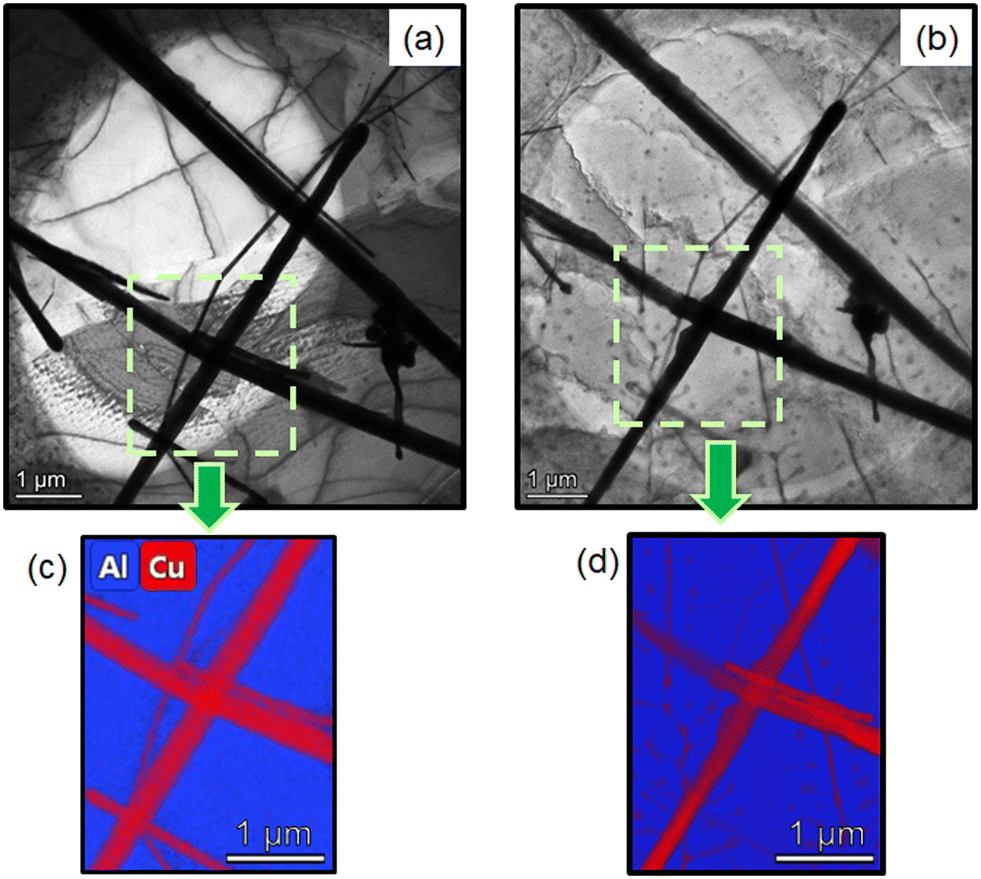 | ||
| Fig. 3 Results of melting and alloying for the Al–Cu system. The same region of the Al–Cu sample before and after alloying is shown. In the foreground are the Cu NWs, and in the background is the sample. (a) and (b) Show BFTEM micrographs. (c) and (d) Display the corresponding EDS maps of the sample. | ||
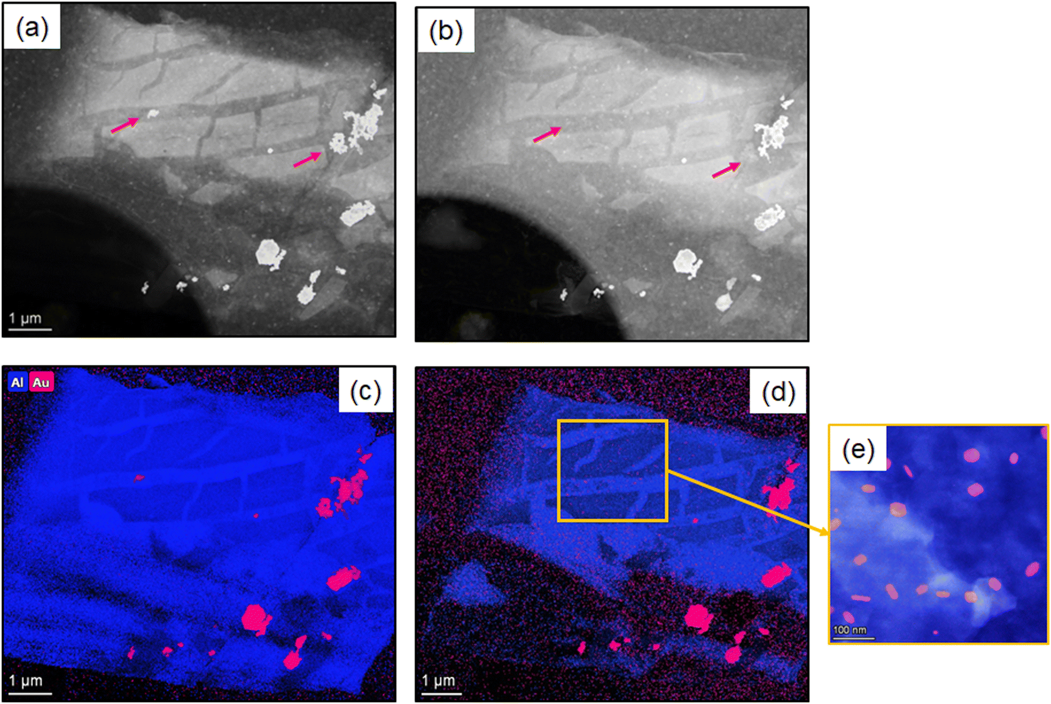 | ||
| Fig. 4 Results of melting and alloying for the Al–Au system. HAADF STEM micrographs and EDX maps before and after melting are shown in the insets (a)–(d), respectively. Some Au NP clusters (highlighted by the red arrows) are no longer present after the melting experiment and small nanometric precipitates formed after solidification, which are presented in the inset (e). Note that the speckled pattern in the dark areas is an artifact of the EDX mapping. | ||
For the Al–Cu system, the effects of alloying were more pronounced and well visible by structural dendrite-like features whose formation is most likely due to solidification solute partitioning of Cu. The precipitated phase visible after the alloying experiment is of the type θ-Al2Cu, as revealed by the SAED analysis (Fig. 5). The mixing of the alloying agent occurred regardless of the presence of the oxide layer surrounding the NWs or the Al foil. One possible explanation for this is a thinning of the oxide layers that may occur during heating.40 Similar effects were noted by Coradini et al., who report that Cu NWs sublime through a leak in the oxide layer caused by the thinning of the layer upon heating.41
 | ||
| Fig. 5 Annealing of the Al–Cu system at 440 °C after solution treatment (spike annealing at 537 °C). The image series (a) display HAADF micrographs taken at different times. Image series (b) show the sequence with a high-pass filter applied in the Velox software. (c) and (d) Show the EDX maps of the composition/matrix composition before and after the heat treatment. At the start of the annealing treatment, a different structure compared to the dendritic-like seen in Fig. 3 is observed, followed by the spheroidization and coarsening of Al2Cu-type precipitates (verified with SAED pattern of the precipitates, see insert in series (a) on the right). | ||
In contrast to Al–Cu, the Al–Au system showed only marginal changes after alloying compared to the initial state. However, a couple of NP clusters dissolved after melting Al (as indicated by the red arrows in Fig. 4), which indicates that alloying was carried out with it. At this point, it must be noted that at 660 °C the equilibrium solubility of Au in the melt is much lower when compared with the Cu in the melt. Being it 2.5 at% for Au in Al, and 36 at% for Cu in Al (see phase diagrams in Fig. 7). Alloy formation is likely to be correspondingly more sluggish. Furthermore, it is assumed that a large part of the little alloyed Au remains in a supersaturated solid solution after rapid cooling and is not precipitated.
Heat treatments
Now that it has been shown that the alloying experiment was successful, the phase transformations in the course of heat treatment procedures for each system will be presented. The results show that the alloys synthesized in the TEM exhibit formation of precipitates, in the Al–Cu system as expected Al2Cu, and in the Al–Au system, Al2Au.36,42To ensure that the heat treatment performed as expected, we monitored the composition change of the alloys over time and compared it with a phase diagram. Given the scale of our system, we considered a bulk phase diagram, which is reasonable since only particle sizes smaller than 100 nm show changes in formation temperature. For example, Bajaj et al. showed that the Al–Cu eutectic temperature changes are only significant for particles smaller than 30 nm.43 Since the Al foil in our system falls outside this size range, we did not consider a nanoscale diagram, although there might be minor temperature and solubility shifts. The formation of precipitates in the Al–Cu system at 440 °C, following a spike ‘solution annealing’ at 537 °C, is shown in Fig. 5. After spike solution annealing, i.e. at time t = 0 s, a new structure can be seen. According to the EDX analysis, the Cu content of the alloy is 2.47 at%. As the annealing time progresses, the coalescence and coarsening of the precipitate progress. At the end of the experiment after 300 s, the matrix shows a depletion of Cu to a value of 0.8 at%, which agrees very well with the equilibrium concentration at 440 °C (see Fig. 7). The fact that the precipitates are of Al2Cu type was confirmed by SAED in Fig. 5 in the inset (a).
With the intention of obtaining a clear picture of the precipitate formation in the Al–Au system and to be able to make a comparison of results with the literature, heat treatments were performed at two different temperatures, 460 °C, and 250 °C.
The initial condition for the heat treatments was as-alloyed. Solution annealing was not performed due to the low maximum solubility of 0.26 at%. It is shown in the table in Fig. 6, that after the alloying procedure at least as much Au is present in supersaturated solution as would be the case after solution heat treatment.
 | ||
| Fig. 6 Annealing of the Al–Au system at 460 °C after melting. The image series (a) display HAADF micrographs taken at different times, starting with the as-alloyed state (0 s). (b) and (c) Show the EDX maps of the matrix composition before and after the heat treatment, respectively. At the start of the annealing treatment, precipitates are sporadically present in the Al matrix, followed by the formation of Al2Au-type precipitates and EDS (indicated by the SAED pattern of the precipitates, see insert in c). | ||
We first consider the ageing at 460 °C (Fig. 6). In the initial state at 0 s, sporadic precipitates (possibly primary Al2Au) are already present. As the annealing time increases, the precipitates grow and new ones are formed (see light green arrows in image series (a) and compare images (b) and (c)). Simultaneously, the content of Au in solid solution decreases from 0.13 at% to 0.07 at% after 220 s. The equilibrium state is almost reached, 0.05 at%, see Fig. 7(a).
 | ||
| Fig. 7 Calculated phase diagram of Al–Cu (a and b) and Al–Au (c and d), using the thermochemical software FactSage 8.2.44 (a) and (b) display the Al–Au diagram with two different regions, (a) presenting the limit solubility of the liquid phase at 660 °C, and (b) showing the limit of solubility in the solid phase. (c) and (d) Show the Al–Cu, whereas (c) depicts the solubility of Au in the liquid phase, and (d) in the solid phase. The numbers indicate the solubility limits at the corresponding annealing temperatures. | ||
Bourgeois et al.38 report on the bulk and interfacial structures of the Al2Au after precipitation annealing at 250 °C of an Al–Au alloy with 0.2 at% Au. After an annealing time of 3600 s, they observe the formation of plate-like Al2Au precipitates with a side length of about 50 nm. A comparable result can be observed in our 250 °C annealing experiment (Fig. 8).
 | ||
| Fig. 8 HAADF image illustrating the formation of plate-like Al2Au structures during a heat treatment for 3600 s hour at 250 °C. | ||
Conclusions
The study of the application of in situ nanoalloying and its utilization for subsequent heat treatment direct within a transmission electron microscope has shown promising results in the examination of the effect of metallurgical processes using nanomaterials and Al matrix as precursors. Herein, the results showed that Au nanoparticles and Cu nanowires can undergo melting and alloying on an Al substrate within an electron microscope. In line with thermodynamic predictions and a higher solubility of Cu in Al, the effect of melting and alloying was more pronounced in the Al–Cu system. The formation of a precipitate composed of likely Al2Cu was observed in the Al–Cu system. However, the mixing of the alloying agent occurred regardless of the presence of an oxide layer surrounding the NPs/NWs or the Al foil for both systems. The Al–Au system showed comparatively fewer changes, but alloying was achieved and precipitate formation could be observed. Overall, these results suggest that TEM-based in situ melting and alloying is a valuable technique for studying the effects of metallurgical procedures on nanomaterials and can provide crucial information for the development of advanced materials with improved properties while undertaking alloying, heat treatment, and characterization steps entirely within the TEM. Therefore, we can conclude that the in situ TEM nanoalloying technique herein presented is a new “lab-on-a-chip” approach for the emerging science of nanometallurgy. Nevertheless, more studies are needed to define a more controlled way of introducing the alloying species to the Al sheet enabling better control of the outcome material composition.Author contributions
Conceptualization, D. S. R. Coradini, M. A. Tunes, S. Pogatscher; methodology, D. S. R. Coradini, M. A. Tunes, S. Pogatscher, T. Kremmer; formal analysis, D. S. R. Coradini, P. J. Uggowitzer, S. Pogatscher, P. Dumitraschkewitz; investigation, D. S. R. Coradini; writing—original draft, D. S. R. Coradini; writing—review and editing, D. S. R. Coradini, M. A. Tunes, S. Pogatscher, P. J. Uggowitzer, S. Samberger, P. Willenshofer; resources, T. Kremmer, S. Pogatscher; visualization, D. S. R. Coradini, S. Samberger, P. Willenshofer, P. J. Uggowitzer; supervision, S. Pogatscher.Conflicts of interest
There are no conflicts to declare.Acknowledgements
This project has received funding from the European Research Council (ERC) under the European Union's Horizon 2020 research and innovation programme (grant agreement No 757961). All authors are grateful for the Austrian Research Promotion Agency (FFG) within the project 3DnanoAnalytics (FFG-No. 858040). MAT acknowledges support from the Laboratory Directed Research and Development (LDRD) program at the Los Alamos National Laboratory under contract 20200689PRD2. The authors would like to thank Mr. Matthias Honner, Ms. Nadine Tatzreiter, Ms. Carmen Schlager and Mr. Florian Frick for their support with the Cu NWs solution preparation.Notes and references
- N. Thakur, T. R. Das, S. Patra, M. Choudhary and S. K. Shukla, Electrochemical Sensors, Elsevier, 2022, pp. 241–259 Search PubMed.
- L. Yi, L. Zhao, Q. Xue, H. Cheng, H. Shi, J. Fan, S. Cai, G. Li, B. Hu and L. Huang, et al. , Lab Chip, 2020, 20, 931–941 RSC.
- M. Medina-Sánchez, S. Miserere and A. Merkoçi, Lab Chip, 2012, 12, 1932–1943 RSC.
- A. Merkoçi and J. P. Kutter, Lab Chip, 2012, 12, 1915–1916 RSC.
- D. Huang, Z. Lu, Q. Xu, X. Liu, W. Yi, J. Gao, Z. Chen, X. Wang and X. Fu, RSC Adv., 2021, 11, 21405–21413 RSC.
- A. C. Ferrari, F. Bonaccorso, V. Fal'Ko, K. S. Novoselov, S. Roche, P. Bøggild, S. Borini, F. H. Koppens, V. Palermo and N. Pugno, et al. , Nanoscale, 2015, 7, 4598–4810 RSC.
- S. Zhu, M. T. Nguyen and T. Yonezawa, Nanoscale Adv., 2021, 3, 4626–4645 RSC.
- R. Kumar, S. Ranjith, H. Balu, D. Bharathi, K. Chandan and S. S. Ahmed, UPI J. Pharm. Med. Health Sci., 2022, 39–43 Search PubMed.
- C. López de Dicastillo, E. Velásquez, A. Rojas, A. Guarda and M. J. Galotto, Compr. Rev. Food Sci. Food Saf., 2020, 19, 1760–1776 CrossRef PubMed.
- M. Distaso, et al. , Acta Innov., 2020, 57–66 Search PubMed.
- O. Ivanova, C. Williams and T. Campbell, Rapid Prototyp. J., 2013, 19, 353–364 CrossRef.
- O. D. Neikov and N. Yefimov, Handbook of non-ferrous metal powders: technologies and applications, Elsevier, 2009 Search PubMed.
- W. Lu and C. M. Lieber, Nat. Mater., 2007, 6, 841–850 CrossRef CAS PubMed.
- S. Zhang, Mater. Today, 2003, 6, 20–27 CrossRef CAS.
- P. Iqbal, J. A. Preece and P. M. Mendes, in Nanotechnology: The Top-Down and Bottom-Up Approaches, John Wiley and Sons, Ltd, 2012 Search PubMed.
- M. M. Schneider and J. M. Howe, Acta Mater., 2017, 133, 224–229 CrossRef CAS.
- A. Mamalis, J. Mater. Process. Technol., 2007, 181, 52–58 CrossRef CAS.
- L. M. Hoyos-Palacio, D. P. C. Castro, I. C. Ortiz-Trujillo, L. E. B. Palacio, B. J. G. Upegui, N. J. E. Mora and J. A. C. Cornelio, J. Mater. Res. Technol., 2019, 8, 5893–5898 CrossRef CAS.
- B. Ravi, S. Sampath, R. Gambino, J. Parise and P. Devi, J. Therm. Spray Technol., 2006, 15, 701–707 CrossRef.
- L. Staiger, T. Kratky, S. Günther, A. Urstoeger, M. Schuster, O. Tomanek, R. Zbořil, R. W. Fischer, R. A. Fischer and M. Cokoja, Nanoscale, 2021, 13, 15038–15047 RSC.
- W. Yan, H. Jiang, W. Yi, C. Zhao, Y. Xia, H. Cong, L. Tang, G. J. Cheng, J. He and H. Deng, Mater. Chem. Front., 2022, 6, 2796–2802 RSC.
- J. Tang, R. Daiyan, M. B. Ghasemian, S. A. Idrus-Saidi, A. Zavabeti, T. Daeneke, J. Yang, P. Koshy, S. Cheong and R. D. Tilley, et al. , Nat. Commun., 2019, 10, 1–14 CrossRef PubMed.
- R. Ferrando, J. Jellinek and R. L. Johnston, Chem. Rev., 2008, 108, 845–910 CrossRef CAS PubMed.
- G. Marx, Nature, 1966, 211, 22–23 CrossRef.
- H.-T. Tung and A. R. Davoyan, Nano Lett., 2022, 22, 1108–1114 CrossRef CAS PubMed.
- M. Taghavi, M. M. Salary and H. Mosallaei, Nanoscale Adv., 2022, 4, 1727–1740 RSC.
- M. A. Tunes, C. R. Quick, L. Stemper, D. S. Coradini, J. Grasserbauer, P. Dumitraschkewitz, T. M. Kremmer and S. Pogatscher, Materials, 2021, 14, 1085 CrossRef CAS PubMed.
- J. Murray, H. Okamoto and T. Massalski, Bull. Alloy Phase Diagrams, 1987, 8, 20–30 CrossRef CAS.
- H. Okamoto, J. Phase Equilib. Diffus., 2005, 26, 391 CrossRef CAS.
- S. Son, M. Takeda, M. Mitome, Y. Bando and T. Endo, Mater. Lett., 2005, 59, 629–632 CrossRef CAS.
- M. Von Heimendahl, Acta Metall., 1967, 15, 1441–1452 CrossRef CAS.
- W. Miao and D. Laughlin, Metall. Mater. Trans. A, 2000, 31, 361–371 CrossRef.
- L. Stemper, M. A. Tunes, P. Dumitraschkewitz, F. Mendez-Martin, R. Tosone, D. Marchand, W. A. Curtin, P. J. Uggowitzer and S. Pogatscher, Acta Mater., 2021, 206, 116617 CrossRef CAS.
- S. Pogatscher, H. Antrekowitsch and P. J. Uggowitzer, Acta Mater., 2012, 60, 5545–5554 CrossRef CAS.
- D. S. Coradini, M. A. Tunes, T. M. Kremmer, C. G. Schön, P. J. Uggowitzer and S. Pogatscher, npj Mater. Degrad., 2020, 4, 33 CrossRef CAS.
- O. Zobac, A. Kroupa, A. Zemanova and K. W. Richter, Metall. Mater. Trans. A, 2019, 50, 3805–3815 CrossRef CAS.
- G. Piatti and G. Pellegrini, J. Mater. Sci., 1976, 11, 913–924 CrossRef CAS.
- L. Bourgeois, Z. Zhang, J. Li and N. V. Medhekar, Acta Mater., 2016, 105, 284–293 CrossRef CAS.
- P. Dumitraschkewitz, M. A. Tunes, C. R. Quick, D. S. R. Coradini, T. M. Kremmer, P. Ramasamy, P. J. Uggowitzer and S. Pogatscher, Acta Mater., 2022, 239, 118225 CrossRef CAS.
- Z. Zhang and D. Su, Ultramicroscopy, 2009, 109, 766–774 CrossRef CAS PubMed.
- D. Santa Rosa Coradini, M. A. Tunes, P. Willenshofer, C. Quick, T. Kremmer, S. Luidold, P. J. Uggowitzer and S. Pogatscher, Unravelling Nanometallurgy with in Situ Electron-Microscopy: A Case Study with Cu Nanowires, Available at SSRN: https://ssrn.com/abstract=4462257, DOI:10.2139/ssrn.4462257.
- T. Egami, M. Ojha, D. M. Nicholson, D. V. Louzguine-Luzgin, N. Chen and A. Inoue, Philos. Mag., 2012, 92, 655–665 CrossRef CAS.
- S. Bajaj, M. G. Haverty, R. Arróyave and S. Shankar, Nanoscale, 2015, 7, 9868–9877 RSC.
- C. W. Bale, P. Chartrand, S. Degterov, G. Eriksson, K. Hack, R. B. Mahfoud, J. Melançon, A. Pelton and S. Petersen, Calphad, 2002, 26, 189–228 CrossRef CAS.
| This journal is © The Royal Society of Chemistry 2023 |