
 Open Access Article
 This Open Access Article is licensed under a Creative Commons Attribution-Non Commercial 3.0 Unported Licence
On-chip monitoring of toxic gases: capture and label-free SERS detection with plasmonic mesoporous sorbents†
Marta
Lafuente
 ab,
Fernando
Almazán
ab,
Eduardo
Bernad
ab,
Ileana
Florea
c,
Raul
Arenal
ade,
Miguel A.
Urbiztondo
f,
Reyes
Mallada
abg and
Maria P.
Pina
*abg
ab,
Fernando
Almazán
ab,
Eduardo
Bernad
ab,
Ileana
Florea
c,
Raul
Arenal
ade,
Miguel A.
Urbiztondo
f,
Reyes
Mallada
abg and
Maria P.
Pina
*abg
aInstituto de Nanociencia y Materiales de Aragón (INMA), CSIC-Universidad de Zaragoza, 50009 Zaragoza, Spain. E-mail: mapina@unizar.es
bDepartment of Chemical & Environmental Engineering, Campus Rio Ebro, C/Maria de Luna s/n, 50018 Zaragoza, Spain
cLaboratoire de Physique des Interfaces et des Couches Minces (LPICM), CNRS, Ecole Polytechnique, IP Paris, 91128, Palaiseau Cedex, France
dARAID Foundation, 50018 Zaragoza, Spain
eLaboratorio de Microscopias Avanzadas (LMA), Universidad de Zaragoza, 50018 Zaragoza, Spain
fCentro Universitario de la Defensa de Zaragoza, Carretera Huesca s/n, 50090 Zaragoza, Spain
gNetworking Research Center on Bioengineering, Biomaterials and Nanomedicine, CIBER-BBN, 28029 Madrid, Spain
First published on 20th June 2023
Abstract
The detection of the spread of toxic gas molecules in the air at low concentration in the field requires a robust miniaturized system combined with an analytical technique that is portable and able to detect and identify the molecules, as is the case with surface enhanced Raman scattering (SERS). This work aims to address capability gaps faced by first responders in real-time detection, identification and monitoring of neurotoxic gases by developing robust, reliable and reusable SERS microfluidic chips. Thus, the key performance attributes of a portable SERS detection system that must be addressed in detail are its limit of detection, response time and reusability. To this purpose, we integrate a 3D plasmonic architecture based on closely packed mesoporous silica (MCM48) nanospheres decorated with Au nanoparticle arrays, denoted as MCM48@Au, into a Si microfluidic chip designed and used for preconcentration and label-free detection of gases at a trace concentration level. The SERS performance of the plasmonic platform is thoroughly analyzed using DMMP as a model neurotoxic simulant over a 1 cm2 SERS active area and over a range of concentrations from 100 ppbV to 2.5 ppmV. The preconcentration-based SERS signal amplification by the mesoporous silica moieties is evaluated against dense silica counterparts, denoted as Stöber@Au. To assess the potential for applications in the field, the microfluidic SERS chip has been interrogated with a portable Raman spectrometer, evaluated with temporal and spatial resolution and subjected to several gas detection/regeneration cycles. The reusable SERS chip shows exceptional performance for the label-free monitoring of 2.5 ppmV gaseous DMMP.
Introduction
Nowadays, Surface Enhanced Raman Scattering (SERS) stands out as a powerful and highly sensitive method to probe molecules in the close vicinity of a plasmonic substrate, even at a single-molecule level.1,2 As Raman scattering analytical technique, SERS enables the detection, identification and quantification of target species in complex mixtures based on their unique molecular vibrational fingerprint in a nondestructive and multiplexed manner. In spite of being the oldest known plasmon-enhanced spectroscopy technique, the routine analysis of surfaces and traces of chemical and biological species using SERS is not still widely used in real-world environments3 and making contributions to our daily life.Over the last decade, sustained efforts have been made to push the SERS transition from an intriguing scientific method into a practical technology, as revealed by the growing number of companies commercializing SERS substrates4–9 and the continuous progress that has been made in affordable, robust and portable Raman instrumentation.10–14 In particularly, SERS has great applicability in the area of defense and homeland security,15–18 and more specifically for the detection of extremely toxic nerve agents,19,20e.g., Sarin gas where 10 min exposure at 64 ppbV provokes life-threatening health effects.21 According to the International Forum to Advance First Responder Innovation (IFAFRI), first responders (FRs) still need technologically advanced tools and equipment that are affordable, lightweight, easy to use and innovative so that FRs may rapidly detect, identify and monitor (DIM) hazardous agents and contaminants on the scene in real time to facilitate timely and appropriate actions in the event of a chemical incident.22 Meeting these requirements of end users and addressing their capability gaps using SERS is a way to move the field significantly forward.
SERS platforms combined with microfluidic systems offer a win–win combination as it has been recently reviewed, mainly for liquid phase applications.23,24 Successful results have also already been reported in the gas phase for environmental monitoring, for example in simultaneous bioaerosol sampling and real time SERS analysis,25 and for the detection of trace levels of explosive vapors within a continuously flowing gas stream.26 Considering the low number of vapor molecules available per unit volume and the frequently encountered weak interactions with the metal surface, gas collection efficiency is an essential criteria for SERS platform design in gas sensing applications. This claim is even more important when dealing with highly diluted gaseous mixtures of nerve agents27 due to their small cross sectional values.28 When target molecules do not show any affinity for the plasmonic surface, the most common strategy is to increase their fraction within the illuminated area. This strategy involves the incorporation of functional coatings on the SERS active surface to promote its physical or chemical adsorption.27,29 The sticking probability30 of the target analytes is also utilized for the microfluidic chip design to maximize the fluid–solid interfacial area.
Microporous and mesoporous materials have great potential in the development of efficient SERS platforms for gas sensing because their huge and highly ordered porosity allows selective adsorption and preconcentration of analytes. The latest advances in the field of SERS-active nanoparticle/metal–organic-framework (MOF) hybrids have been reviewed by Huang et al.31 In a recent work, we validated the use of thin films made from close-packed core–shell Au@Ag nanorods individually encapsulated within a ZIF-8 (zeolitic imidazolate framework) for early SERS detection of chemical warfare agents (CWAs).27 In that work, we reported the experimental detection, in ambient air using a portable Raman spectrometer, of 2.5 ppmV of dimethyl methylphosphonate (DMMP, simulant of sarin gas) and 76 ppbV of 2-chloroethyl ethyl sulfide (CEES, simulant of mustard gas) with response times of 21 s and 54 s, respectively.
Examples of gas sensing with microfluidic SERS chips in the absence of an active liquid medium are rarely encountered in the literature. The array-assisted SERS microfluidic chip developed by Yang et al.32 combines a PDMS (polydimethylsiloxane) chip with a prism array patterned in the microfluidic channel and Au@Ag-nanocubes@ZIF8 nanostructures. The Ag surface has cysteamine anchored on it as an aldehyde-specific recognition molecule to capture the gas. The recorded limit of detection value was 1 ppbV for benzaldehyde and 3-ethylbenzaldehyde in air. Herein, we propose an alternative concept based on mesoporous silica nanospheres decorated with Au nanoparticles (Au NPs), which not only aims to boost the preferential concentration/enrichment of the target molecules over the interfering molecules but also to exploit their dynamic sorption properties for real time detection in practical applications. In addition to preconcentration-based signal amplification, our microfluidic Si chip allows long-term monitoring while maintaining its SERS efficiency well during multiple “detection-heating” cycles thanks to the higher thermal stability of the silica in comparison to the MOF.
This manuscript explores the integration of mesoporous silica spheres, individually decorated with Au NPs, in microfluidic Si chips for the continuous, real-time and quantitative SERS detection of nerve gases at trace levels. The detection occurs under ambient conditions without the need for prior physical collection or sample conditioning (Fig. 1). The preconcentration of target molecules is accomplished through the accumulation of adsorbed molecules both in the silica mesopores, and in close proximity to the SERS-active sites dispersed on the external silica surface. A special focus is devoted to the reusability of the microfluidic SERS chip, an important property for evaluating the usefulness of a SERS technique in practical applications. Finally, in an attempt to characterize the potential adoption of the platform by FRs, preliminary results carried out with hand-held Raman equipment are discussed.
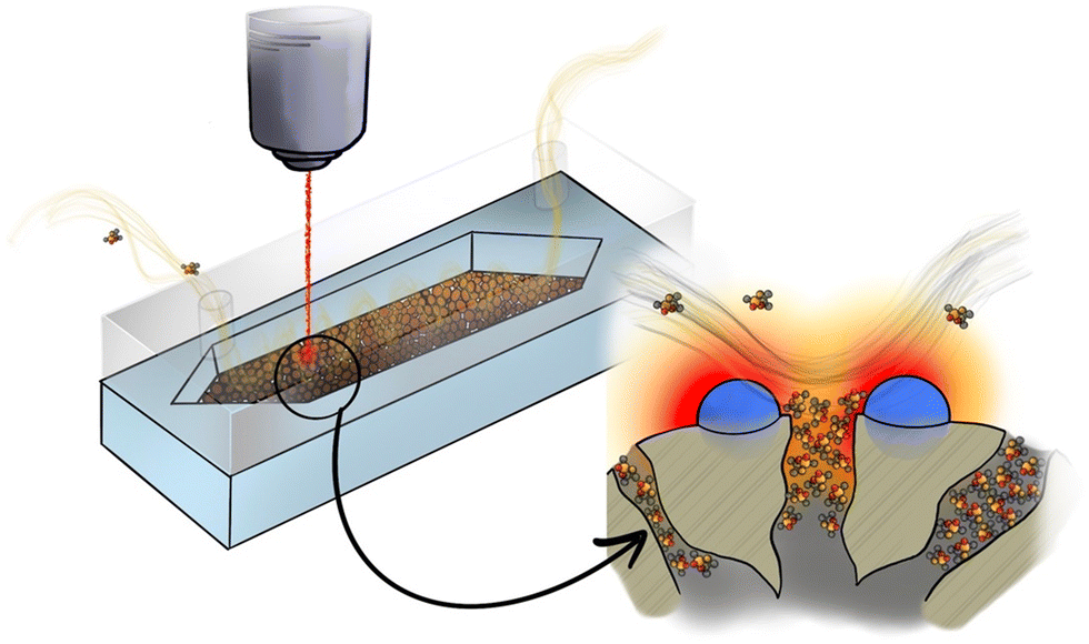 | ||
| Fig. 1 Illustration of the preconcentration effect and efficient SERS examination of the target analyte. The variation of the target analyte concentration in the proximity of the plasmonic mesoporous sorbent embedded in the microfluidic SERS chip is shown. | ||
Unlike previous publications on SERS gas sensing, this work significantly contributes to the simultaneous achievement of the following milestones: i) label free detection of toxic compounds thanks to preconcentration-based SERS signal amplification facilitated by the mesoporous silica moieties; ii) portable SERS detection with handheld Raman instrumentation thanks to the integration of the core–shell plasmonic sorbent within a silicon microfluidic chip; iii) real-time detection/monitoring of toxic vapors/gases thanks to the dynamic sorption properties exhibited by the microfluidic SERS chip; and iv) cost-effectiveness for practical applications thanks to the reusability of the microfluidic SERS chip.
Experimental
Materials
Cetyltrimethylammonium bromide (CTAB, ≥99%), tetraethyl orthosilicate (TEOS, 98%), triblock copolymer Pluronic® F127 (F127), 3-aminopropyl-triethoxysilane (APTES, 98%), chloroauric acid (HAuCl4·xH2O, ∼50%), sodium hydroxide (NaOH), tetrakis(hydroxymethyl)phosphonium chloride (THPC, 80%), potassium carbonate (K2CO3), formaldehyde (37%), rhodamine 6G (R6G, 99%) and dimethyl methylphosphonate (DMMP, 97%) were purchased from Merck and employed without further purification. Ammonium hydroxide solution (NH4OH, 28–30% NH3) and hydrochloric acid (HCl, 37%) were also purchased from Merck and toluene, dichloromethane, and diethylether were purchased from Fisher Chemical. Potassium hydroxide (KOH) and absolute ethanol were purchased from PanReac AppliChem. All aqueous solutions were prepared in Milli-Q water (18.2 MΩ cm−1).Synthesis of gold seeds
Gold seeds (Au-seeds) were synthesized by a modified THPC reduction method.33 This protocol consists of reducing chloroauric acid (HAuCl4) with tetrakis(hydroxymethyl)phosphonium chloride (THPC). Briefly, 1.0 mL of THPC (12 μL of THPC in 1 mL of water) and 0.5 mL of NaOH (1 M) were mixed with 50.0 mL of water under magnetic stirring at room temperature. After 5 min, 2.5 mL of chloroauric aqueous solution (1% wt) was added and when the solution changed from colorless to brown, it was maintained for 10 min more. The Au-seeds colloidal suspension (0.27 mg Au mL−1 nominal content) was stored at 4 °C.Synthesis of mesoporous silica particles (MCM48)
The spherical MCM48 nanoparticles were synthesized by a modified protocol of Kim and co-workers.34 For this purpose, 0.5 g of CTAB and 2.0 g of F127 were mixed in 95.0 mL of water. Once dissolved, 43.0 mL of absolute ethanol and 11.5 mL of NH4OH were added at room temperature. After that, 1.93 mL of TEOS was added into the mixture. The reaction was maintained for 4 h at a magnetic stirring rate of 650 rpm. Then, the mixture was kept in static conditions for 24 h at room temperature and a dark-environment for further silica condensation. The white solid product was recovered by centrifugation, then washed three times with water and dried overnight at 70 °C. The final template-free MCM48 nanoparticles were obtained after calcination at 550 °C in air for 6 h with a heating rate of 1 °C min−1.Synthesis of dense silica nanoparticles
This synthesis was based on the well-known Stöber process.35 In summary, 3.0 mL of NH4OH and 1.5 mL of TEOS were added to 50.0 mL of absolute ethanol under magnetic stirring and at room temperature. The solution completely changed color from colorless to white in 270 min.Synthesis of core–shell MCM48@Au plasmonic mesoporous sorbents
The preparation of core–shell mesoporous silica–gold nanoparticles MCM48@Au involves three main steps (the same for their dense counterparts). The first step is the synthesis and functionalization of the silica nanoparticles with amine groups. The second is the Au seeding of the silica nanoparticles and the last step of the procedure involves the controlled growth of Au-seeds over the aminated silica surface (see Fig. 2(a)). Following a similar protocol, core–shell nanostructures based on dense silica were prepared, denoted as Stöber@Au for the remainder of this work.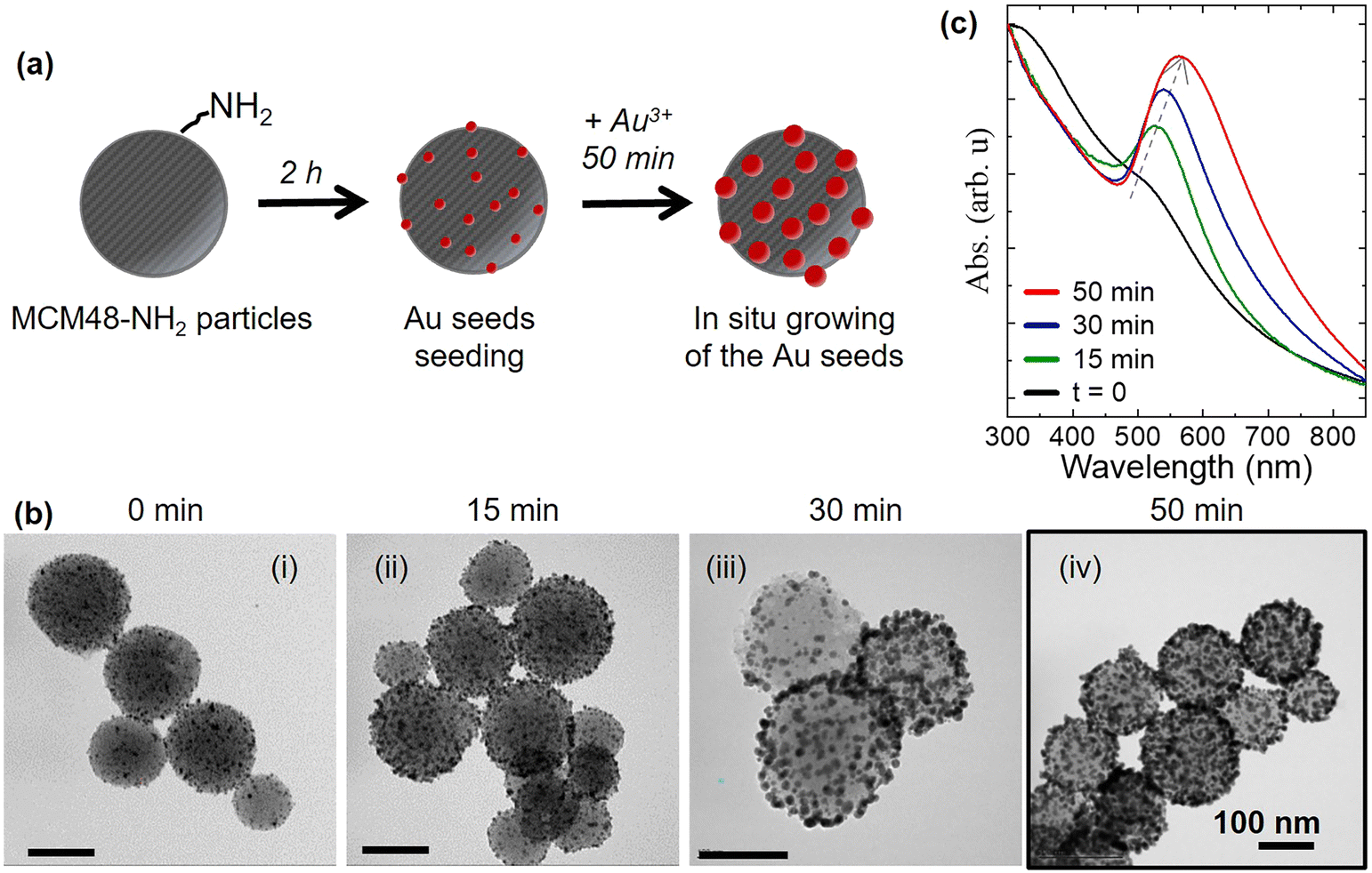 | ||
Fig. 2 (a) Scheme showing the three main steps of the core–shell MCM48@Au synthesis. (b) TEM images of the resulting nanoparticles and (c) UV-vis-NIR spectra of the amine-MCM48/Au seeds_1![[thin space (1/6-em)]](https://www.rsc.org/images/entities/char_2009.gif) :10 data set as a function of the Au seed growth time (0, 15, 30 and 50 min). Highlighted image (iv) is illustrative of the MCM48@Au plasmonic sorbent used in this work. Scale bar is 100 nm. :10 data set as a function of the Au seed growth time (0, 15, 30 and 50 min). Highlighted image (iv) is illustrative of the MCM48@Au plasmonic sorbent used in this work. Scale bar is 100 nm. | ||
:1 v/v) mixture and dried at 50 °C for 12 h.
:20.6 Au:Si molar ratio) and the pH of the mixture was adjusted to around 2.5 by addition of HCl. The resulting mixture was kept at room temperature for 2 h in a dark environment. The collected product was centrifuged 3 times at 4000 rpm for 20 min and the obtained pellet was redispersed in 5 mL of water (3.4 mg SiO2 mL−1 nominal content). This step was also carried out with Au-seed suspension volumes of 3 and 6 mL.
:4.8 Au:Si molar ratio). The reaction time was fixed at 50 min at a stirring rate of 670 rpm. Then, the MCM48@Au nanoparticle solution was centrifuged at 2500 rpm for 15 min and redispersed in 1 mL of water. The growth step was also carried out for shorter periods (15 and 30 min) resulting in three different Au-seeded amine-MCM48 solutions.
Microfluidic SERS chip fabrication
The microfabrication process for the functional microfluidic SERS chip comprises five different steps: cavity etching, MCM48@Au plasmonic sorbent incorporation, microdevice sealing, heater element integration and inlet/outlet port mechanization. A detailed explanation of the fabrication process, described in our previous work,37 is provided in section S1 of the ESI† and Fig. S1.1. A similar process was carried out for the fabrication of the “MCM48-Au seeds” microfluidic chip, which is mainly used here for reference purposes.SERS substrates preparation
In this work, silica@Au films supported on a Si/SiO2 wafer (0.4 cm × 0.8 cm) were prepared to assess on the analytical enhancement factor (AEF) and for preliminary detection experiments of DMMP in the gas phase at different concentrations. Likewise, SERS substrates supported on Borofloat (0.4 cm × 0.8 cm) were used for determining the UV-vis-NIR extinction spectra. Thus, the substrates were sequentially washed for 10 min in acetone, isopropanol and water in an ultrasound bath and finally dried under an N2 stream. Afterwards, silica@Au nanoparticles were deposited by spin-coating (25 cycles of a 0.15 wt% Si ethanolic solution) on Borofloat supports or by an opaline method (0.05 wt% Si aqueous solution) on Si/SiO2 supports.Materials characterization
The size and morphology of the core–shell nanostructures were examined throughout the synthesis procedure using transmission electron microscopy (TEM, FEI TECNAI T20). The samples were prepared by adding a drop of ultrasonicated ethanol suspension onto copper carbon holey grids. Z-potential measurements of the solutions in 1 mM KCl were carried out in a Brookhaven 90 plus using Zeta Pals software. Scanning electron microscopy (SEM, CSEM-FEG Inspect) images were used to characterize the functional microchannel coated with MCM48@Au nanoparticles. The UV-vis-NIR extinction spectra of the silica@Au nanoparticles in aqueous suspensions were acquired on a UV-vis double beam spectrophotometer Jasco V670. A Varian Cary 50 spectrometer was used for the UV-vis-NIR spectra of the silica@Au films supported on glass. Fourier-transform infrared (FTIR) spectra were measured with a Bruker VERTEX 70 instrument with a Golden Gate diamond attenuated total reflectance (ATR) accessory to assess the silica surface amination. Spectra were recorded by averaging 40 scans in the range 6000–400 cm−1. Nitrogen physisorption isotherms of the MCM48 nanoparticles before and after amination were studied with a Micromeritics TriStar 300 analyzer. The samples were degassed at 13.3 kPa and 200 °C for 8 h. The commercial software, MicroActive v4.03 (Micromeritics), was used for data processing. The surface area was evaluated according to the Brunauer–Emmett–Teller (BET) theory in the relative pressure range from 0.05 to 0.20. The pore volume and pore size distribution were evaluated using non-local density-functional theory (NLDFT). The thickness of the sorbent coating in the microfluidic SERS chip was evaluated by contact profilometry using a mechanical profilometer P-6 Stylus Profiles (KTA Tencor) with a 5 μm diamond stylus tip with a 60° cone angle. For each microfluidic chip, 3 to 5 randomly selected cross sections were measured 3 times and its thickness was calculated as an average of these measurements.Electron tomography characterization of core–shell MCM48@Au nanostructures
The electron tomography measurements were performed using the scanning transmission electron microscopy (STEM) mode of a probe-corrected STEM FEI Titan-Low-Base 60-300 operating at 80 keV (equipped with a X-FEG® gun and Cs-probe corrector (CESCOR from CEOS GmbH)). The large inner radius of the high-angle annular dark-field (HAADF) detector used for the acquisition of the tilt series allowed us to deem that the intensity in the corresponding images is proportional to the atomic number (Z), having access to a Z-contrast.38–41 The acquisition of the STEM-HAADF tilt series was performed using the tomography Inspect-3D software. The HAADF tilt series was acquired by tilting the specimen in an angular range of ±70° using an increment of 2° in the equal mode, thus giving a total number of images in the tilt series equal to 71. The recorded images of the tilt series were spatially aligned using a two-step alignment; a first rough alignment by cross correlating consecutive images, followed by a fine step alignment using the Au NPs. Both procedures were implemented in the IMOD software.42 For the volume calculations, we used algebraic reconstruction techniques (ART) implemented in the TomoJ plugin working in the ImageJ software.43,44 Finally, the visualization and the analysis of the final volumes were carried out using the displaying capabilities and the isosurface rendering method in the Slicer software.45Raman and SERS measurements
Raman and SERS measurements were carried out using a confocal WITec Alpha 300 (spectral resolution 2 cm−1) and a portable Raman BWTEK i-Raman® Pro (spectral resolution 6 cm−1). Both instruments were coupled to a 785 nm laser line. The measurements with the benchtop WITec equipment were recorded with a 0.1 mW laser power, exposure time of 1 s and a 20× objective (spot diameter, 1.92 μm; 0.034 mW μm−2). The SERS spectra recorded with the Raman BWTEK were measured at 0.044 mW μm−2 and an integration time of 2 s. For the AEF evaluation, the MCM48@Au and Stöber@Au films supported on Si/SiO2 were immersed in R6G solutions (1 μM) and, after air-drying, more than 20 measurements along the SERS substrates were performed and averaged.SERS detection of gaseous DMMP
SERS measurements with both silica@Au systems were conducted in a homemade aluminum chamber (circa 100 μL gas free volume), into which a N2 gas stream of 10 STP cm3 min−1, with the desired concentration of DMMP, was fed continuously.19,27,46 A gaseous stream of DMMP in nitrogen (2.5 ppmV, 12.7 mg m−3) was generated using a calibrated permeation tube (MT-PD-experimental 107-100-7845-HE3-C50, 126.8 ng min−1 ± 4.8 ng min−1 at 80 °C, from VALCO) immersed in a thermostatic bath at a controlled temperature (80 °C). In the case of lower concentrations of DMMP, Tedlar gas sampling bags were used. These were prepared by the accurate injection of the proper DMMP liquid amount (0.4 μL of DMMP in 10 L of N2) followed by homogenization. Then, DMMP bags with concentrations of 900 ppbV, 250 ppbV and 100 ppbV were prepared by step-by-step dilution with dry N2.27Static DMMP adsorption properties
The as-synthesized and amine-functionalized MCM48 and dense silica nanoparticles were degassed overnight at 150 °C and used to quantify the DMMP adsorption properties when exposed to its vapor pressure at 20 °C i.e. 739 ppmV (3748 mg m−3) in a sealed container. Aliquots of the exposed materials were taken and analyzed using thermogravimetry on a TA Instruments TGA-Q5000 (using N2 up to 600 °C at 10 °C min−1 as heating rate).Dynamic DMMP adsorption experiments on the microfluidic SERS chip
Breakthrough-type adsorption experiments on the SERS chips were carried out at room temperature. While circulating the DMMP/N2 stream at 10 STP cm3 min−1 with 16 mg m−3 DMMP through the microdevice, the outlet stream was analyzed online using gas chromatography coupled with a mass spectrometer (Shimadzu GCMS-QP2010). In order to characterize the dynamic sorption properties, the experiment was performed until the outlet concentration (Cx) was equal to the feed concentration (C0). For this work, the breakthrough point is considered as the moment where Cx/C0 = 0.1, which implies that the adsorbent is becoming saturated and unable to trap all the analyte molecules carried by the feed gas. A detailed explanation of the breakthrough testing is provided in section S1 of the ESI† and Fig. S1.2 and S1.3.Continuous monitoring of gaseous DMMP on the microfluidic SERS chip with a portable Raman spectrometer
The SERS performance of the microfluidic SERS chip coated with MCM48@Au was evaluated by continuous monitoring of 2.5 ppmV DMMP (14 mg m−3) in N2 10 STP cm3 min−1 with temporal and spatial resolution using a portable i-Raman® Pro. At the end of the experiment, the SERS-chip was regenerated by sweeping at 10 STP cm3 min−1 with dry N2 for 5 min followed by degassing at 200 °C using the heating coil printed on the backside of the chip (DC voltage supply 15 V). For reference purposes, similar experiments were conducted with an uncoated chip (blank experiment), and with microfluidic chips coated with “MCM48-Au seeds.”Results and discussion
Synthesis and characterization of MCM48@Au plasmonic mesoporous sorbents
The core–shell MCM48-Au nanostructure has a spherical mesoporous silica particle (MCM48) as the core, to provide the surface area for adsorption and concentration of target molecules, and an array of individual Au NPs randomly distributed on the outer surface to provide the SERS enhancement. The synthesis of such MCM48@Au nanoparticles involves three main steps as schematically shown in Fig. 2(a).The first step is the synthesis of spherical MCM48 type mesoporous silica particles with a size distribution centered at 187 ± 34 nm, pore size of 3.5 nm and a BET surface area of 1237 m2 g−1 (see Fig. S2.1 and Table S2.1 in section S2 of ESI†). Afterwards, the silica nanoparticles were functionalized with amine groups by 3-aminopropyl-triethoxysilane (APTES) grafting in order to: i) facilitate the anchoring of Au seeds on the external surface of the silica by electrostatic interactions; and, ii) enhance the DMMP sorption thanks to the increased hydrophilicity of the aminated silicas.47,48 In fact, the presence of co-adsorbed water vapor could benefit DMMP uptake due to the shift of the energy distribution probability curve, attributed to the DMMP affinity, towards the water molecules.49 Specific peaks in the FTIR spectra (see Fig. S2.2 in section S2 of the ESI†) evidenced the presence of specific organic functionalities after the aminosilane grafting. The aminated sample, denoted as MCM48-NH2, exhibits a broad band at 1560 cm−1 and additional peaks from 2800 to 3300 cm−1 characteristic of the N–H bending of primary amines and C–H stretching vibrations, respectively. In addition, the band around 1450 cm−1 can be attributed to the N–H bending vibration of the ammonium cations.
The second step is the electrostatic anchoring of the pre-formed gold seeds (3–4 nm in size) on the MCM48-NH2 surface. The electrostatic anchoring is performed at 2.5 pH as the Au seeds exhibit a negative surface charge (−12 mV) and the MCM48-NH2 particles a positive charge (+50 mV), as measured by zeta potential analysis (see Fig. S2.3 in section S2 of the ESI†).
The last step involves the controlled growth of the Au seeds over the silica surface to obtain Au NPs with an intense localized surface plasmon resonance (LSPR) peak in the visible range, while preserving the access to the MCM48 mesopores. This is an important improvement over previous works50–52 where silica particles are individually encapsulated within a nonporous gold shell. Via delicate optimization of the reaction conditions, the particles undergo controlled growth and the formation of a continuous gold coating is prevented, maintaining the free access of vapors to the aminated mesopores. Three MCM48-NH2/Au seed solutions with different volumetric ratios (1:3, 1:6 and 1:10) were tested in order to achieve a uniform distribution of Au seeds over the MCM48-NH2 surface (see Fig. S2.4 in section S2 of the ESI†). A solution containing particles of “MCM48-Au seeds” was mixed with the growth solution for reaction times varying from 0 to 50 min. Fig. 2(b) shows representative TEM images of the resulting SERS probes whilst Fig. 2(c) shows the normalized extinction spectra as a function of reaction time. The LSPR characterization is shown in Fig. 2(c) and in Fig. S2.4 in section S2 of the ESI.† As can be observed, the MCM48@Au nanoparticles from the 1:10 ratio grown for 50 min show a more intense and narrower LSPR peak while avoiding a continuous Au shell (see Fig. 2(b) panel (iv)). This increase in intensity of the resonant absorption peak with the growth time is accompanied by a red shift of the LSPR spectrum (maximum of absorption, from 527 nm to 585 nm) due to the plasmonic coupling between adjacent Au NPs and the formation of Au aggregates on the silica surface. Accordingly, the sample obtained by re-growing the MCM48/Au seeds_1:10 for 50 min (Fig. 2(b) (iv)) was selected for the fabrication of the microfluidic SERS chip studied in this work.
The nanoarchitecture of the selected SERS probe was investigated using electron tomography. Fig. 3(a)–(c) display three different STEM-HAADF representative projections at three different tilt angles extracted from the tilt series used to reconstruct the volume. In these images, one can easily identify two different contrast regions corresponding to the MCM48 silica particle; and, respectively, a high amount of Au NPs which seem to be located on the external surface of the MCM48 silica particle. The analysis of some typical slices taken at different depths and orientations through the corresponding reconstructed volume confirms this, as shown in Fig. 3(d) and (e). The corresponding 3D model, Fig. 3(f) and (g), depicts the homogeneous distribution of the Au NPs on the surface of the MCM48 material.
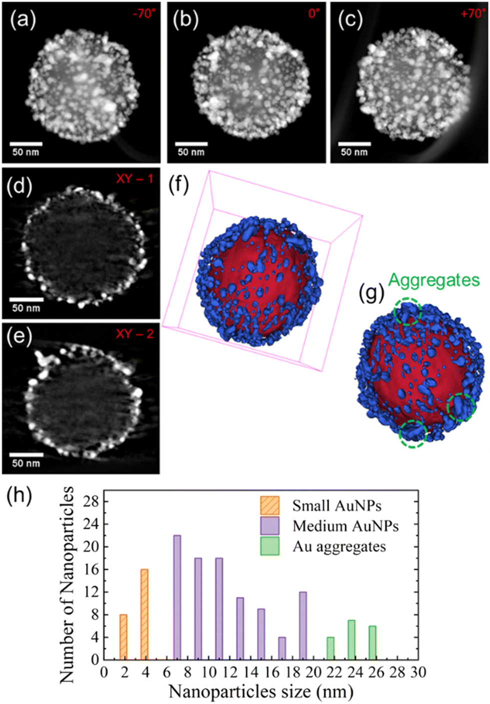 | ||
| Fig. 3 (a)–(c) 2D projections extracted from the STEM-HAADF tilt series used to reconstruct the volume of the core–shell MCM48@Au nanostructure, for three different tilt angles marked in red (−70°, 0° and +70°). (d) and (e) Typical orthoslices through the reconstructed volume, showing the exact localization of Au NPs on the external surface of the spherical mesoporous silica particle. (f) and (g) 3D model representation of the system obtained from the reconstruction of the STEM-HAADF tilt series employing a data segmentation procedure and a surface-rendering method. The surface of the mesoporous silica MCM48 material is represented in red and the Au NPs in blue. The Au NPs located on the external surface of the silica particle can form aggregates, highlighted by the dashed green circles in Fig. 3(g). (h) Histogram obtained from the tomogram volume reconstruction showing the size distribution of the Au NPs as well as the distribution of the aggregates. | ||
A detailed analysis of the obtained volume allowed the size of the anchored Au NPs to be estimated to be varying in a range between 2.5 nm (pristine seeds) and 15 nm (grown seeds). Fig. 3(h) shows the size distribution of both Au nanostructures, the individual Au NPs and the aggregates. Thus, the size distribution of these Au nanostructures is responsible for the broad plasmonic response band in observed aqueous solution and depicted in Fig. 2(c). Moreover, by counting the pixels located at the interface of the MCM48 material and the Au NPs, we estimated a 40% coverage of the external surface of the MCM48-NH2 particle by the Au nanostructures.
SERS performance of the silica@Au substrates: AEF evaluation and detection of gaseous DMMP
The optical response of the two silica@Au supported films on Borofloat substrates (see Fig. S3.1 in section S3 of the ESI†) reveals a broadening of the original plasmonic band and a clearly noticeable red shift due to plasmonic coupling between adjacent core–shell nanoparticles in agreement with the multilayer-type structure observed by SEM (see Fig. S3.2 in section S3 of the ESI†).Preliminary evaluation of the SERS efficiency of the mesoporous sorbent versus that of the dense probe was accomplished by evaluation of the analytical enhancement factor, AEF, using rhodamine 6G (R6G) and its characteristic Raman peak at 1510 cm−1 (attributed to C–C stretching mode). The comparison of the SERS spectra of an aqueous 1 μM R6G solution of both the MCM48@Au and Stoöer@Au supported films (see Fig. S3.3 in section S3 of the ESI†) was utilized to elucidate the differences in SERS-active area. The SERS activity of the MCM48@Au substrate outperforms its Stöber@Au counterpart. The 99% confidence interval for the R6G SERS intensity average value at 1510 cm−1 is 4556 ± 436 cts for MCM48@Au versus 1029 ± 154 cts for the Stöber@Au substrate (see Table S3.1 in section S3 of the ESI†).
The textural properties of the synthesized MCM48 silica, i.e. its highly ordered porosity (0.43–0.95 cm3 g−1) on the nanometer scale (2.7–3.5 nm pore size) and its large specific surface area (1052–1237 m2 g−1) vs. that of its dense silica counterpart (12 m2 g−1) (see Table S2.1 in section S2 of the ESI†), are the main drivers responsible for the spontaneous adsorption of target molecules on its pore walls. Herein, we intend to leverage the unique characteristics of the MCM48 particles in our core–shell nanostructure, thanks to preconcentration-based signal amplification, to provide a more intense SERS response compared to that exhibited by analogous probes based on dense silica spheres.
To assess the effectiveness of our silica core for preconcentration, the DMMP uptake was evaluated for MCM48, MCM48-NH2 and dense SiO2 systems, when exposed to 739 ppmV at 20 °C in dry air (see Fig. S2.5 in section S2 of the ESI†). In these experiments, after exposure to DMMP, the mesoporous silicas clearly desorbed a greater amount than the dense silica (up to 11 and 18 times more for the MCM48-NH2 and MCM48 samples, respectively). In the case of MCM48-NH2, the DMMP uptake value was 133.7 mg g−1 (see Table S2.2 in section S2 of the ESI†).
Fig. 4(a) shows the SERS spectrum of DMMP in N2 at 2.5 ppmV recorded for the MCM48@Au and Stöber@Au supported films using a customized gas chamber19,27,46 and benchtop Raman instrumentation. The characteristic Raman fingerprint of DMMP is clearly distinguishable in the SERS spectrum of the MCM48@Au substrate and up to six characteristic Raman features (denoted as (a) to (f) for the remainder of this work) are displayed. The Raman band assignments of DMMP are described in Table S3.2 in section S3 of the ESI.† As can be observed, the relative intensity of the SERS peaks differs from those acquired under normal Raman conditions due to the preferential orientation of the DMMP molecules adsorbed on the silica surface.48 The more intense bands at 710 cm−1 and 1270 cm−1, denoted as bands (a) and (f) in Fig. 4(a), are assigned to the symmetrical stretching of the P–C and P![[double bond, length as m-dash]](https://www.rsc.org/images/entities/char_e001.gif) O bonds, respectively. On the contrary, the DMMP spectrum recorded on the Stöber@Au substrate scarcely shows the vibrational band characteristic of the P–C stretching.
O bonds, respectively. On the contrary, the DMMP spectrum recorded on the Stöber@Au substrate scarcely shows the vibrational band characteristic of the P–C stretching.
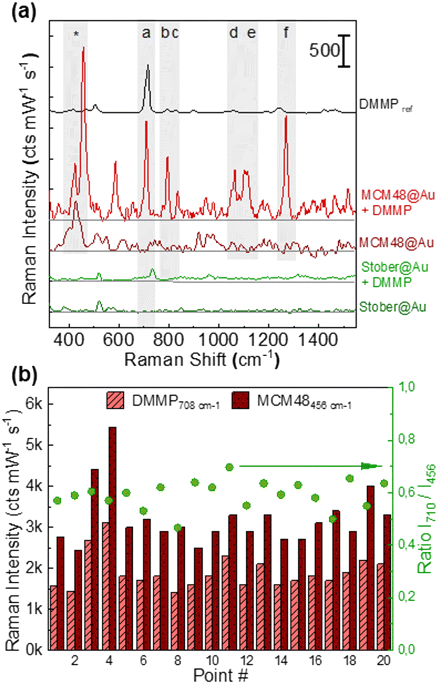 | ||
| Fig. 4 (a) Average SERS spectra of DMMP (2.5 ppmV) recorded on the MCM48@Au and Stöber@Au supported films compared to the Raman fingerprint of pure DMMP in the liquid phase and blank MCM48@Au and Stöber@Au samples, respectively. The characteristic Raman band of MCM48-NH2 used as a Raman internal standard is labelled with *. (b) Spatial distribution of the DMMP peak (at 710 cm−1) and MCM48 (at 456 cm−1) over 20 different points of the surface of the MCM48@Au substrate. Right axis (green dots): SERS intensity ratio between peak 710 cm−1 of DMMP and 456 cm−1 of MCM48. | ||
When comparing the normalized SERS signal at 710 cm−1 acquired on both silica@Au platforms in the presence of 2.5 ppmV of DMMP, the response exhibited by MCM48@Au is almost one order of magnitude higher than that obtained over the dense counterpart, 1575 ± 365 cts mW−1 s−1vs. 172 ± 41 cts mW−1 s−1. Once again, these results demonstrate that the larger surface area of MCM48-NH2 substantially increases the intensity of the SERS response due to a denser population of DMMP molecules in the vicinity of the Au nanostructures. Remarkably, it was possible to use the intense MCM48-NH2 peak recorded at 456 cm−1 (Si–O mode53), labelled with (*) in Fig. 4(a), as a Raman internal standard since it does not overlap with the SERS signal of DMMP. As previously demonstrated for core–shell Au@Ag@ZIF8 nanostructures,27,32 the use of a ratiometric SERS response, I710/I456, improves the spatial uniformity of the SERS response. Fig. 4(b) shows the characteristic SERS signal of DMMP and MCM48-NH2 over a centimeter scale area of the substrate (20 random spots). In fact, the use of a ratiometric SERS response, I710/I456, allows the correction of local variations in the SERS signals improving the relative standard deviation (RSD) of the SERS measurements, i.e. 0.58 ± 0.08 (15%).
Moreover, the sensitivity of the MCM48@Au multilayer platform was tested by monitoring the SERS response as a function of the DMMP concentration ranging from 100 to 2500 ppbV, see Fig. S2.6 in section S2 of the ESI.† The preconcentration-based SERS signal amplification provided by the mesoporous silica moieties allows detection of up to 100 ppbV of DMMP. The average SERS spectra show the expected gradual intensity increase with DMMP concentration, corresponding to a higher number of molecules adsorbed on the MCM48-NH2 core and, consequently, in close vicinity of the plasmonic surface. In all cases, the average standard deviation of the SERS signal at 710 cm−1 remains below 20%.
Plasmonic mesoporous sorbents integrated in microfluidic SER chip: fabrication and evaluation of dynamic sorption properties towards DMMP
The microfluidic SERS chip is composed of two parts: a microfluidic channel on a Si substrate coated with the MCM48@Au plasmonic mesoporous sorbent and a glass substrate suitable for Raman interrogation (see Fig. 5(a)). The novelty of the approach herein presented is that the incorporation of the functional material is accomplished before sealing the device, thus enabling the controlled deposition of the material and its quantification.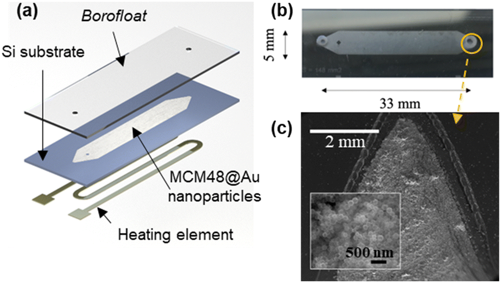 | ||
| Fig. 5 (a) Scheme of the components of the microfluidic SERS chip (43 mm × 15 mm, length × width). (b) Photograph of the microfluidic SERS chip before assembly of the connections. (c) Top view of the microfluidic channel after spin-coating of MCM48@Au nanoparticles. Inset: MCM48@Au coating at higher magnification. | ||
The spin-coating conditions lead to dense films with close-packed silica-Au nanoparticles distributed along the cavity (see Fig. 5(b) and (c)). Microchannel depth and thickness of the SERS active coating have been confirmed by profilometry (see Fig. S1.4 in section S1 of the ESI†). Specifically, the SERS active coating of the microfluidic chip is circa 2.1 μm thick, i.e., more than 10 layers of close-packed assembly of MCM48@Au nanostructures; and the estimated mass loading is 527 μg. In our previous work,27 a monolayer of close-packed Au@Ag@ZIF-8 nanoparticles, homogeneously distributed over the whole substrate with a surface coverage circa 60%, is applied for CWAs SERS detection in the vapor phase. This work, by contrast, deploys a 3D plasmonic architecture to better utilize the laser excitation volume, while maximizing the analyte capture and its accumulation in the vicinity of the enhancing metallic surface.
Dynamic retention capacities towards DMMP vapors were estimated from breakthrough curve analysis, as presented in Fig. 6(a). In addition, a blank experiment with a sealed and uncoated microdevice was carried out for baseline subtraction. A stream of 10 STP cm3 min−1 at a concentration of 16 mg m−3 DMMP in dry N2 at room temperature was continuously fed to the microfluidic chip during the adsorption stage. The MCM48@Au modified microfluidic SERS chip exhibits the breakthrough point after having processed a total feed volume of 190 STP cm3. This value implies a DMMP dynamic adsorption capacity of 3.2 μg (circa 6 mg g−1).
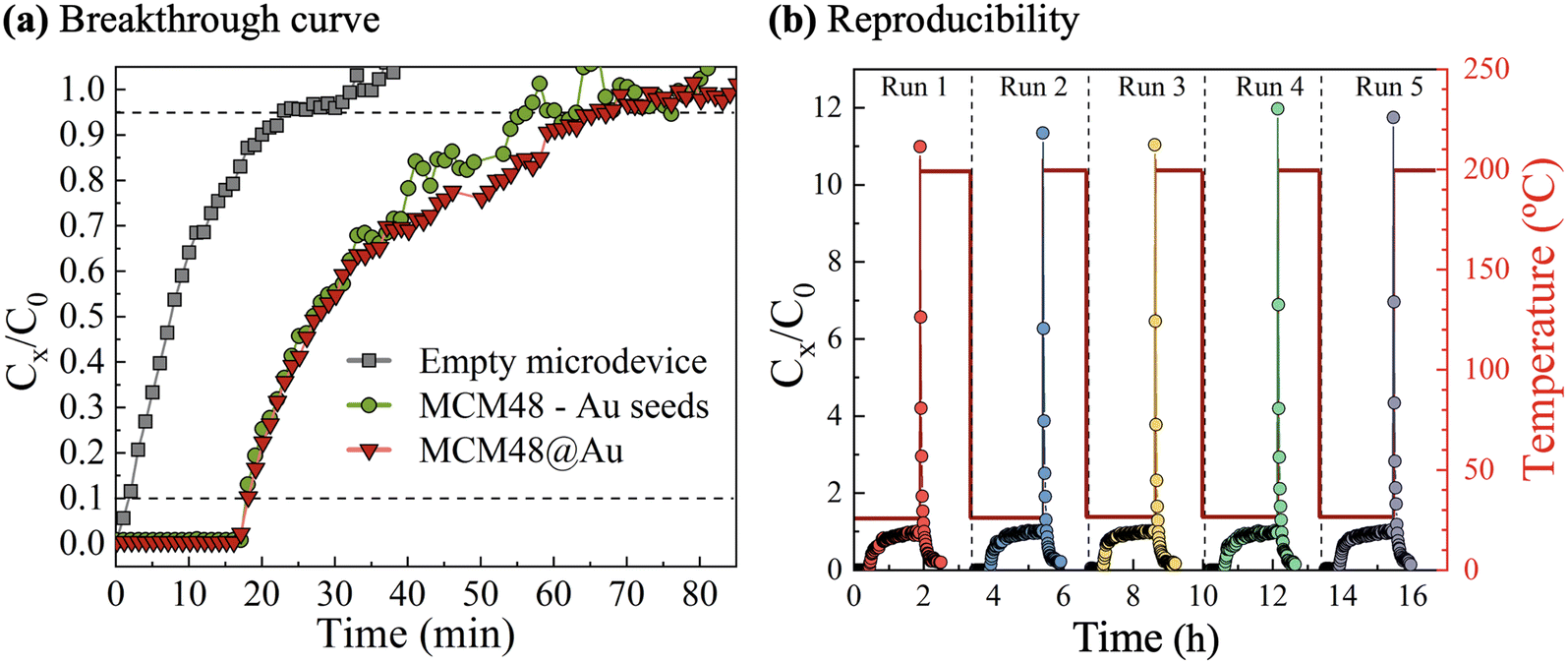 | ||
| Fig. 6 MCM48 coated microfluidic chips for DMMP preconcentration: (a) comparative breakthrough testing for microdevices containing MCM48 nanoparticles with Au seeds on the surface (denoted as MCM48 – Au seeds) and MCM48@Au plasmonic nanoparticles (MCM48@Au); (b) adsorption (room temperature) – desorption (200 °C) performance of the SERS microfluidic chip when exposed to cyclic operation. Experimental conditions: 16 mg m−3 (3 ppmV) of DMMP in 10 STP cm3 min−1 of dry N2. The performance of an empty microdevice, i.e. uncoated, is also plotted for reference purposes. | ||
Interestingly, a nearly identical breakthrough profile was recorded on microfluidic chips coated with mesoporous silica spheres decorated with Au seeds 3–4 nm in size (i.e., not yet subjected to the growth procedure). This observation demonstrates that the access of DMMP vapors to MCM48 mesopores is not hindered by the Au nanostructures dispersed on the external silica surface.
The reusability of the microfluidic SERS chips was confirmed by assessment of the sorption properties upon exposure to several DMMP sorption–desorption cycles (see Fig. 6(b)) carried out according to the experimental protocol described in Fig. S1.3 in section S1 of the ESI.† According to online GC-MS measurements of the outlet stream, the regeneration of the plasmonic sorbent is almost achieved after 60 min at 200 °C under dry N2, in agreement with the baseline recovery of the GC-MS signal (see Fig. S1.5 in section S1 of the ESI†).
Continuous monitoring of gaseous DMMP using the microfluidic SERS chip and a portable Raman spectrometer
The SERS spectra recorded for DMMP at the ppb level on MCM48@Au (Fig. S2.6 in section S2 of the ESI†), combined with the DMMP adsorption dynamics in the microfluidic chip (Fig. 6(a)), prompted us to test its suitability for real-time monitoring in practical applications. Thus, continuous detection of 2.5 ppmV of DMMP was attempted using the microfluidic SERS chip and a portable Raman spectrometer, as would be the case in a realistic emergency scenario. It should be noted that the microfluidic SERS chip previously employed in the consecutive DMMP adsorption–desorption cycles was used for the SERS measurements described in this section to corroborate the robustness of the microsystem.First, the spatial uniformity of the SERS response registered on the microfluidic chip was verified via measurements with the portable Raman spectrometer and calculation of the ratiometric signal, I710/I456, at five different positions on a 4 mm pitch along the microfluidic channel (see Fig. 7(a)).
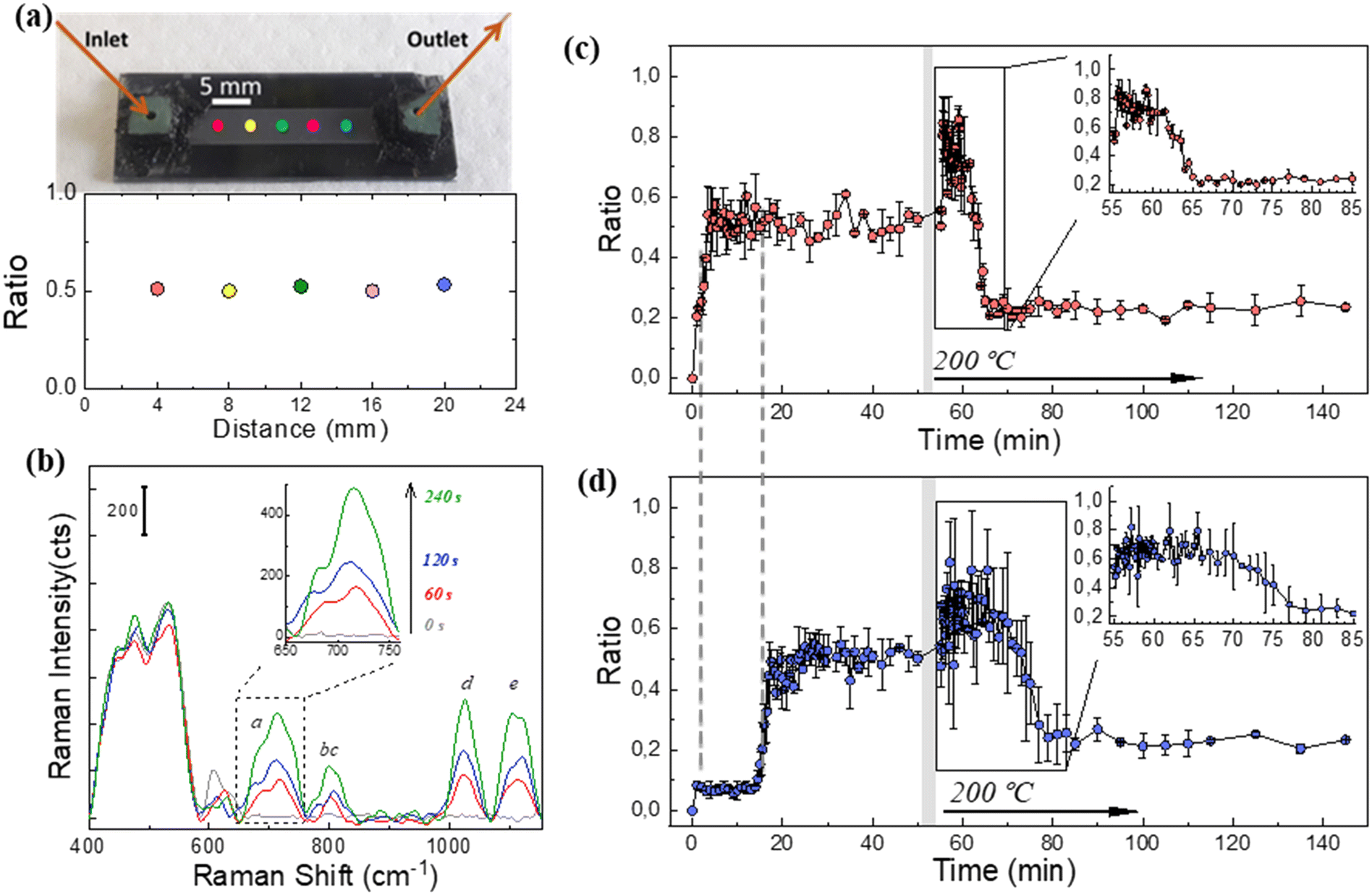 | ||
| Fig. 7 Detection of DMMP vapours (2.5 ppmV) using the microfluidic SERS chip and a portable Raman spectrometer: (a) optical image of the microfluidic SERS chip and SERS intensity ratio, I710/I456, recorded at the indicated positions in the presence of 2.5 ppmV DMMP under stationary conditions. (b) Evolution of the SERS spectra of DMMP measured at the entrance of the microfluidic SERS chip as a function of time. (c) and (d) Evolution of the ratiometric SERS signal during the adsorption/desorption cycle measured at the inlet (c) and outlet (d) zones of the microfluidic SERS chip, respectively. In both (c) and (d), the enlarged section corresponds to the beginning of the desorption cycle. For clarity, in (c) and (d), a grey shadow area has been included to indicate the chip sweeping with N2 previous to heating at 200 °C. | ||
Then, the evolution of the DMMP fingerprint versus exposure time was recorded. Fig. 7(b) shows the SERS spectrum measured at the entrance of the chip for exposure times of up to 240 s. In fact, stationary conditions on the SERS active surface are reached at this time. In this work, due to the high signal to noise ratio (see inset in Fig. 7(b)), the response time t50% is defined as the time to reach the 50% of the maximum SERS signal. Accordingly, the t50% value is 120 s; validating a fast response of the microfluidic chip towards DMMP 2.5 ppmV.
Fig. 7(c) and (d) show the resolved time SERS responses at the inlet and outlet zones of the microfluidic chip throughout the DMMP adsorption (at room temperature) and desorption process (at 200 °C), respectively. The time evolution profile of the SERS intensity ratio (I710/I456) recorded at the inlet and outlet is rather similar, although shifted 19 min in accordance with the DMMP breakthrough curves shown in Fig. 6(a). The ratiometric signal at the outlet remains unchanged during the first 10–15 min of the desorption cycle (see inset of Fig. 7(d) and S1.5 in section S1 of the ESI†) in agreement with a sustained release of accumulated DMMP molecules inside the silica mesopores. This effect is attributed to our core–shell architecture for which the electromagnetic field density distribution is at its maximum at the external surface of the MCM48 particle where the SERS active centers are dispersed, and through which the desorbed DMMP molecules from its inner pores travel. After desorbing at 200 °C for more than 30 min, the ratiometric SERS signal does not recover its baseline value recorded at room temperature. We mainly attribute this behavior to the temperature dependence of the SERS response, i.e., the dielectric functions of silica and gold, respectively.
The reusability of the SERS chip, an important issue for those chips that have a certain complexity and significant cost, as is the case with ours, is also addressed. The in situ regeneration of the MCM48@Au SERS probes is achieved by thermal cycling for several minutes following a similar protocol to that used during breakthrough testing. This procedure provokes the release of the adsorbed molecules from the silica mesopores and leads to a refreshed system for subsequent Raman interrogation. Online GC-MS measurements of the outlet stream from the chip indicate that the DMMP molecules are mostly desorbed from the plasmonic sorbent within 60 min. The time evolution profile of the fractional coverage of the sorption sites (θ) evaluated from GC-MS analysis (refer to eqn (S1.1) in section S1 of the ESI† for details on θ calculations) is plotted against the SERS intensity ratio (I710/I456) recorded at the outlet of the chip for an intercomparison of both analytical techniques (see Fig. S1.5†). As an example, at 30 min desorption time the estimated value of θ is 0.17, whereas the ratiometric SERS response (I710/I456) is 0.25. Accordingly, the herein developed microfluidic SERS chip goes beyond the state of the art in miniaturized and reusable devices for label-free and rapid identification and quantification of neurotoxic gases at ppm level with a portable Raman spectrometer.
Conclusions
In this work, we have demonstrated the efficiency of an MCM48@Au mesoporous plasmonic sorbent that consists of a core–shell structure made of mesoporous silica surrounded by a plasmonic Au shell. The efficiency with which this material concentrates molecules in its pores was validated against the same core–shell architecture with a dense silica core. The deployment of this nanostructure has revealed clear advantages for the less studied field of Surface Enhanced Raman Scattering (SERS) detection of gaseous molecules at low concentration, where the number of molecules per unit volume decreases dramatically. The porous core acts as a sponge for adsorbing and concentrating the gaseous analyte in the proximity of the SERS-enhancing gold nanostructures. In fact, the uptake of the simulant gas nerve agent dimethyl methylphosphonate (DMMP) on aminated mesoporous silica particles is up to 10 times higher than on its dense silica counterparts. In addition, the characteristic Raman peak of MCM48-NH2 at 456 cm−1 acts as an internal standard that enables quantitative detection by correcting for signal fluctuation between analyzed spots.In a further step, we have developed a robust, reliable and reusable SERS platform for detection in the field by combining the MCM48@Au nanostructured material and a microfluidic Si chip. The microfluidic chamber contains the plasmonic sorbent that concentrates the gaseous analyte, and at the same time its glass window enables Raman interrogation with portable equipment. Remarkably, the SERS chip demonstrates good capabilities to detect 2.5 ppmV DMMP using portable Raman equipment with a t50 response time of 120 s. We have verified the on-chip monitoring at various points of the microfluidic channel, at a scale of several centimeters, and followed the time-resolved concentration of DMMP along the adsorption process. The regeneration of the SERS platform is achieved by degassing at 200 °C using the heating coil printed on the backside of the chip. The SERS efficiency is well-maintained after multiple detection–regeneration cycles enabling several uses of the microfluidic chip without losing its performance.
Author contributions
M. L. and E. B. synthesized and characterized the nanoparticles and prepared the SERS substrates; M. L. designed and performed the SERS experiments, data analysis and prepared the manuscript; F. A. designed and fabricated the microfluidic system and characterized the adsorption properties of the nanoparticles and prepared the manuscript: I. F. and R. A. recorded and analyzed the STEM-HAADF images and revised the manuscript; M.-A. U. provided suggestions for the adsorption experiments and the interpretation of data; R. M. and M.-P. P. proposed the original idea, guided the experiments, and wrote the manuscript. All authors have given approval to the final version of the manuscript.Conflicts of interest
The authors declare no competing financial interests.Acknowledgements
Authors are grateful for financial support from: the European Union’s Horizon 2020 research and innovation program under grant agreements no. 883390 (H2020-SU-SECU-2019 SERSing Project), no. 823895 (H2020-MSCA-RISE-2018 SENSOFT), no. 823717 (ESTEEM3 Project); PID2019-108660RB-I00 and PID2019-104739GB-100 funded by MCIN/AEI/10.13039/501100011033; and Government of Aragon (grant numbers E13_20R, T57-17R FEDER, EU).References
- M. J. Natan, Faraday Discuss., 2006, 132, 321–328 RSC.
- J. Langer, D. J. de Aberasturi, J. Aizpurua, R. A. Alvarez-Puebla, B. Auguié, J. J. Baumberg, G. C. Bazan, S. E. J. Bell, A. Boisen, A. G. Brolo, J. Choo, D. Cialla-May, V. Deckert, L. Fabris, K. Faulds, F. J. G. de Abajo, R. Goodacre, D. Graham, A. J. Haes, C. L. Haynes, C. Huck, T. Itoh, M. Käll, J. Kneipp, N. A. Kotov, H. Kuang, E. C. Le Ru, H. K. Lee, J. F. Li, X. Y. Ling, S. A. Maier, T. Mayerhöfer, M. Moskovits, K. Murakoshi, J. M. Nam, S. Nie, Y. Ozaki, I. Pastoriza-Santos, J. Perez-Juste, J. Popp, A. Pucci, S. Reich, B. Ren, G. C. Schatz, T. Shegai, S. Schlücker, L. L. Tay, K. G. Thomas, Z. Q. Tian, R. P. van Duyne, T. Vo-Dinh, Y. Wang, K. A. Willets, C. Xu, H. Xu, Y. Xu, Y. S. Yamamoto, B. Zhao and L. M. Liz-Marzán, ACS Nano, 2020, 14, 28–117 CrossRef CAS PubMed.
- R. Panneerselvam, G. K. Liu, Y. H. Wang, J. Y. Liu, S. Y. Ding, J. F. Li, D. Y. Wu and Z. Q. Tian, Chem. Commun., 2017, 54, 10–25 RSC.
- SERS Substrates|SERSitive: Accurate SERS Substrates, https://sersitive.eu/, (accessed 3 May 2022) Search PubMed.
- SERS Substrates-SERStrates of superior quality, Strong and uniform Raman signal, https://www.silmeco.com/, (accessed 3 May 2022) Search PubMed.
- Ocean Insight, Applied Spectral Knowledge | Spectrometers, https://www.oceaninsight.com/, (accessed 3 May 2022) Search PubMed.
- Hamamatsu Photonics, Home, https://www.hamamatsu.com/jp/en.html, (accessed 3 May 2022).
- Welcome to HORIBA, https://www.horiba.com/int/, (accessed 3 May 2022) Search PubMed.
- PiCO SERS, U.S Patented l More than 10 Times Stronger, https://www.picofd.com/, (accessed 3 May 2022) Search PubMed.
- FirstDefender™ RM Chemical Identification System, https://www.thermofisher.com/order/catalog/product/FIRSTDEFENDERRM, (accessed 3 May 2022) Search PubMed.
- NanoRam® Handheld Raman Spectrometer for Material ID, https://bwtek.com/products/nanoram/, (accessed 3 May 2022) Search PubMed.
- Serstech, Indicator Kit – Handheld Raman Spectrometer, https://serstech.com/our-offer/serstech-100-indicator/, (accessed 3 May 2022) Search PubMed.
- Bruker, BRAVO Handheld Raman Spectrometer, https://www.bruker.com/en/products-and-solutions/infrared-and-raman/raman-spectrometers/bravo-handheld-raman-spectrometer.html, (accessed 3 May 2022) Search PubMed.
- Lightnovo, miniRaman spectrometer, https://lightnovo.com/lightnovo-products/raman-spectrometer/, (accessed 20 October 2022) Search PubMed.
- R. S. Golightly, W. E. Doering and M. J. Natan, ACS Nano, 2009, 3, 2859–2869 CrossRef CAS PubMed.
- B. Sharma, R. R. Frontiera, A. I. Henry, E. Ringe and R. P. van Duyne, Mater. Today, 2012, 15, 16–25 CrossRef CAS.
- J. Choi, J. H. Kim, J. W. Oh and J. M. Nam, Nanoscale, 2019, 11, 20379–20391 RSC.
- A. P. Lister, W. J. Sellors, C. R. Howle and S. Mahajan, Anal. Chem., 2021, 93, 417–429 CrossRef CAS PubMed.
- M. Lafuente, I. Pellejero, V. Sebastián, M. A. Urbiztondo, R. Mallada, M. P. Pina and J. Santamaría, Sens. Actuators, B, 2018, 267, 457–466 CrossRef CAS.
- A. Hakonen, P. O. Andersson, M. Stenbæk Schmidt, T. Rindzevicius and M. Käll, Anal. Chim. Acta, 2015, 893, 1–13 CrossRef CAS PubMed.
- United States Environmental Protection Agency (EPA), Agent GB (Sarin) Results – AEGL Program, https://www.epa.gov/aegl/agent-gb-sarin-results-aegl-program, (accessed 3 August 2021) Search PubMed.
- The International Forum to Advance First Responder Innovation (IFAFRI), Statement of objectives (SOO) for rechnologies related to: the ability to rapidly identify hazardous agents and contaminants, https://www.internationalresponderforum.org/capability-gap-3-statement-objectives, (accessed 3 August 2021) Search PubMed.
- R. Panneerselvam, H. Sadat, E. M. Höhn, A. Das, H. Noothalapati and D. Belder, Lab Chip, 2022, 22, 665–682 RSC.
- D. Choi, T. Kang, H. Cho, Y. Choi and L. P. Lee, Lab Chip, 2009, 9, 239–243 RSC.
- J. Choi, J. Lee and J. H. Jung, Biosens. Bioelectron., 2020, 169, 112611 CrossRef CAS PubMed.
- B. D. Piorek, S. J. Lee, M. Moskovits and C. D. Meinhart, Anal. Chem., 2012, 84, 9700–9705 CrossRef CAS PubMed.
- M. Lafuente, S. de Marchi, M. Urbiztondo, I. Pastoriza-Santos, I. Pérez-Juste, J. Santamaría, R. Mallada and M. Pina, ACS Sens., 2021, 6, 2241–2251 CrossRef CAS PubMed.
- S. D. Christesen, Appl. Spectrosc., 1988, 42, 318–321 CrossRef CAS.
- L. E. Kreno, N. G. Greeneltch, O. K. Farha, J. T. Hupp and R. P. Van Duyne, Analyst, 2014, 139, 4073–4080 RSC.
- K. B. Biggs, J. P. Camden, J. N. Anker and R. P. V. Duyne, J. Phys. Chem. A, 2009, 113, 4581–4586 CrossRef CAS PubMed.
- C. Huang, A. Li, X. Chen and T. Wang, Small, 2020, 16, 1–17 Search PubMed.
- K. Yang, S. Zong, Y. Zhang, Z. Qian, Y. Liu, K. Zhu, L. Li, N. Li, Z. Wang and Y. Cui, ACS Appl. Mater. Interfaces, 2020, 12, 1395–1403 CrossRef CAS PubMed.
- D. G. Duff, A. Baiker and P. P. Edwards, Langmuir, 1993, 9, 2301–2309 CrossRef CAS.
- T. W. Kim, P. W. Chung and V. S. Y. Lin, Chem. Mater., 2010, 22, 5093–5104 CrossRef CAS.
- W. Stöber, A. Fink and B. Ernst, J. Colloid Interface Sci., 1968, 26, 62–69 CrossRef.
- H. Nigar, B. Garcia-Baños, F. L. Peñaranda-Foix, J. M. Catalá-Civera, R. Mallada and J. Santamaria, AIChE J., 2016, 62(2), 547–555 CrossRef CAS.
- F. Almazán, I. Pellejero, A. Morales, M. A. Urbiztondo, J. Sesé, M. P. Pina and J. Santamaría, J. Micromech. Microeng., 2016, 26, 084010 CrossRef.
- L. Liu, U. Díaz, R. Arenal, G. Agostini, P. Concepción and A. Corma, Nat. Mater., 2017, 16, 132–138 CrossRef CAS PubMed.
- F. L. Deepak, A. Mayoral and R. Arenal, Advanced Transmission Electron Microscopy: Applications to Nanomaterials, Springer International Publishing, 2015 Search PubMed.
- K. Sohlberg, T. J. Pennycook, W. Zhou and S. J. Pennycook, Phys. Chem. Chem. Phys., 2015, 17, 3982 RSC.
- L. Uson, J. L. Hueso, V. Sebastian, S. Irusta, M. Arruebo, J. Santamaria, R. Arenal and I. Florea, Catal. Commun., 2017, 100, 93–97 CrossRef CAS.
- D. N. Mastronarde, J. Struct. Biol., 1997, 120, 343–352 CrossRef CAS PubMed.
- R. Gordon, R. Bender and G. T. Herman, J. Theor. Biol., 1970, 29, 471–481 CrossRef CAS PubMed.
- C. MessaoudiI, T. Boudier, C. O. S. Sorzano and S. Marco, BMC Bioinf., 2007, 8, 288 CrossRef PubMed.
- 3D Slicer image computing platform | 3D Slicer, https://www.slicer.org/, (accessed 2 June 2021) Search PubMed.
- M. Lafuente, D. Sanz, M. A. Urbiztondo, J. Santamaría, M. P. Pina and R. Mallada, J. Hazard. Mater., 2020, 384, 121279 CrossRef CAS PubMed.
- T. Suteewong, H. Sai, M. Bradbury, L. A. Estroff, S. M. Gruner and U. Wiesner, Chem. Mater., 2012, 24, 3895–3905 CrossRef CAS.
- P. Xu, S. Guo, H. Yu and X. Li, Small, 2014, 10, 2404–2412 CrossRef CAS PubMed.
- F. Almazán, M. A. Urbiztondo, P. Serra-Crespo, B. Seoane, J. Gascon, J. Santamaría and M. P. Pina, ACS Appl. Mater. Interfaces, 2020, 12, 42622–42633 CrossRef PubMed.
- L. Gomez, M. Arruebo, V. Sebastian, L. Gutierrez and J. Santamaria, J. Mater. Chem., 2012, 22, 21420–21425 RSC.
- C. Wang, M. Li, Q. Li, K. Zhang, C. Wang, R. Xiao and S. Wang, RSC Adv., 2017, 7, 13138–13148 RSC.
- K. Wang, Y. Wang, C. Wang, X. Jia, J. Li, R. Xiao and S. Wang, RSC Adv., 2018, 8, 30825–30831 RSC.
- C. Moisii, M. D. Curran, L. J. van de Burgt and A. E. Stiegman, J. Mater. Chem., 2005, 15, 3519–3524 RSC.
Footnote |
| † Electronic supplementary information (ESI) available: Microfabrication of the microfluidic SERS chips. Characterization of the SERS microfluidic chips: profilometer analyses and breakthrough testing. Synthesis and characterization of plasmonic silica sorbents: TEM images, nitrogen physisorption analyses, pore volume distribution, FTIR-IR characterization, Z-potential. DMMP uptake values estimated by TGA analyses. Optical and SERS characterization of the supported silica@Au films. Determination of analytical enhancement factor (AEF). Experimental vibrational frequencies of pure DMMP. See DOI: https://doi.org/10.1039/d3lc00136a |
| This journal is © The Royal Society of Chemistry 2023 |