
 Open Access Article
 This Open Access Article is licensed under a Creative Commons Attribution-Non Commercial 3.0 Unported Licence
Integration of silicon chip microstructures for in-line microbial cell lysis in soft microfluidics†
Pavani Vamsi Krishna
Nittala‡§
 ad,
Allison
Hohreiter§
bd,
Emilio
Rosas Linhard
ab,
Ryan
Dohn
b,
Suryakant
Mishra¶
ad,
Abhiteja
Konda||
c,
Ralu
Divan
c,
Supratik
Guha
ad and
Anindita
Basu
*b
ad,
Allison
Hohreiter§
bd,
Emilio
Rosas Linhard
ab,
Ryan
Dohn
b,
Suryakant
Mishra¶
ad,
Abhiteja
Konda||
c,
Ralu
Divan
c,
Supratik
Guha
ad and
Anindita
Basu
*b
aPritzker School of Molecular Engineering, The University of Chicago, Chicago, IL 60637, USA
bDepartment of Medicine/Section of Genetic Medicine, The University of Chicago, Chicago, IL 60637, USA. E-mail: onibasu@uchicago.edu
cCenter for Nanoscale Materials, Argonne National Laboratory, Lemont, IL 60439, USA
dMaterials Science Division, Argonne National Laboratory, Lemont, IL 60439, USA
First published on 5th April 2023
Abstract
The paper presents fabrication methodologies that integrate silicon components into soft microfluidic devices to perform microbial cell lysis for biological applications. The integration methodology consists of a silicon chip that is fabricated with microstructure arrays and embedded in a microfluidic device, which is driven by piezoelectric actuation to perform cell lysis by physically breaking microbial cell walls via micromechanical impaction. We present different silicon microarray geometries, their fabrication techniques, integration of said micropatterned silicon impactor chips into microfluidic devices, and device operation and testing on synthetic microbeads and two yeast species (S. cerevisiae and C. albicans) to evaluate their efficacy. The generalized strategy developed for integration of the micropatterned silicon impactor chip into soft microfluidic devices can serve as an important process step for a new class of hybrid silicon-polymeric devices for future cellular processing applications. The proposed integration methodology can be scalable and integrated as an in-line cell lysis tool with existing microfluidics assays.
Introduction
The use of soft microfluidic devices for cell sorting and genomic profiling is an active area of research and development, with powerful applications in medicine and biological research.1,2 While many microfluidic techniques have been successfully used to study mammalian single-cell genomics, similar studies of microbial cells have been partly limited due to the tough cell walls of many microbial species. This leads to difficulty with in-line cell lysis, which is a critical first step needed to access the cellular contents within the microfluidic circuit. Partial success in single-cell microbial lysis had been achieved using lytic enzymes that target specific components in the cell walls3,4 or on microbes with lower cell wall thickness or strength, e.g., Gram-negative bacteria.5 Mechanical lysis integrated within a microfluidics environment offer a reagent-free lysis of small volumes of sample and have been investigated previously, including nanoscale barbs,6 nano-blades,7 hybrid chemo-mechanical,8 electrochemical,9 or agitation/bead-milling based.10–12 Most works have focused on mammalian cells which do not have a rigid cell wall, though some have addressed bacterial cell lysis.10–12 Reviews of various mechanical lysing approaches may be found in ref. 13–15 and are summarized in Table S1.† A significant issue with the lysing of microbial cells is the toughness of the cell walls of many microbes. At present, there are no rapid, high-throughput lysis techniques that are compatible with soft microfluidic devices and that can be applied to a wide variety of microbial cells, including fungi, bacteria, etc. in an unbiased way. This can be particularly beneficial where a priori knowledge of the species present may be lacking, e.g., microbiome samples.We present a mechanical lysis approach to rupture the microbial cell wall via micropatterned silicon impactor chips integrated within PDMS-based soft microfluidic devices. This approach offers four advantages: 1) it is agnostic to the microbial species; 2) it is fast, lysing cells in less than a minute; 3) unlike the enzymatic lysis approaches, it does not involve any chemical reagents that can potentially interfere with downstream experiments; 4) it can impart very high normal forces (several kN) during the impaction, using piezo-electrically driven impactors.
In this paper, we describe the process flow and fabrication of different micropatterned silicon impactor chips developed for microbial cell lysis and their integration within the soft microfluidics environment. We developed an integrated architecture that combines mechanical drive motion of a micropatterned silicon impactor chip, controlled flow in the microfluidic device, and optical imaging to visualize flow and mechanical impaction. Following initial testing and successful operation of the device (assessed on micron-sized silica and polystyrene beads suspended in water), we perform mechanical lysis of two microbial species, Saccharomyces cerevisiae and Candida albicans, using our approach. The current paper focuses mainly on the process development, fabrication and packaging of the device and its initial testing to demonstrate successful operation using both synthetic beads and microbial cells as test payloads.
We note that this integration approach is generalizable for incorporation of semiconductor chip-based components into soft microfluidic devices and ensures mechanical flexibility of the device while providing leak-proof integration. Such heterogeneous integration and packaging can open a range of new functionalities and capabilities within microfluidics applications well beyond lysis. For example, optical, electrical, electrophoretic or radio frequency interaction with single microbes may enable the development of new sorting, manipulation and spectroscopic profiling techniques.16 With some modification, the current setup may also be employed for microbial single-cell genomics studies.
Experimental setup and methodology
A schematic of the device with integrated micropatterned silicon impactor (Fig. 1a) and instrumentation (Fig. 1b) used for operation are shown. The micropatterned silicon impactor chip is embedded in the soft microfluidic device. An external syringe pump modulates the flow of cells within the microfluidic channel while piezo actuation drives the micropatterned silicon impactor back and forth, crushing the cells or beads against the glass substrate. Fabrication of different micropatterned silicon impactor chip designs and their integration into soft microfluidic devices are described as follows. | ||
| Fig. 1 (a) Schematic showing the microfluidic device with an embedded micropatterned silicon impactor chip, bonded to a glass substrate. A piezoelectric actuator will assist the silicon chip in moving up and down against the glass substrate to crush or lyse the cells. (b) Component diagram of the setup. (c) Custom setup showing the device on a microscope, connected to a pump and piezo actuator. | ||
Fabrication of micropatterned silicon impactor chips
Microstructural features were patterned on Si <100> wafers (Silicon Valley Microelectronics, Cat# SV007) that are 100 mm in diameter and 525 ± 25 μm thick (prior to etching) using optical lithography followed by dry or wet etching. The Si wafers were quartered, sonicated in acetone and isopropanol for 3 min each, and then rinsed in water and dried at 115 °C on a hot plate for 1 min prior to further handling. Patterns used for optical lithography were designed using Siemens L-Edit software and defined via optical lithography using the Heidelberg MLA150 maskless aligner (at 405 nm), with varying photon doses as outlined below. Descum was performed prior to etching and deposition steps using a CS-1701 Nordson March etch tool (Westlake, OH) set to 50 W, 160 mTorr chamber pressure, and with an O2 flow of 24 standard cubic centimeters per minute (sccm) for varying amounts of time detailed later where needed. Chromium deposition (with typical layer thicknesses of 20 nm) was carried out using a Temescal FC-2000 E-beam Evaporator. Deep reactive ion etching (DRIE), BOSCH-like etching,17 and reactive ion etching (RIE) were performed on an Oxford PlasmaLab System 100. In addition, DRIE etching was also carried out using a DRIE tool from PlasmaTherm following the standard Versaline process. Five different types of micropatterned silicon impactor chips were fabricated using the process flows outlined:![[thin space (1/6-em)]](https://www.rsc.org/images/entities/char_2009.gif) :3 v/v Developer AZ 351 (MicroChemicals GmbH, Germany):deionized (DI) water for 22 s, rinsed in DI water and hard-baked for 3 min at 115 °C. The sample was treated with a weak O2 plasma (descum) for 30 s to remove any resist residue in the developed regions after the lithography (Fig. 2b) and then transferred to the RIE system to etch the Si/SiO2. For this, a 500 W inductively coupled plasma (ICP) was used with the lower electrode (platen) at 25 W, chamber process pressure at 20 mTorr and the electrode temperature of 20 °C (Fig. 2c). The etch time was typically 30 min with an O2 flow of 1.0 sccm and a CHF3 flow of 55 sccm. The resist mask was then removed in Microposit resist remover 1165 (Dupont, Wilmington, DE) via a 6 h immersion. The remaining structures were then wet etched anisotropically in a 30% KOH solution at 90 °C,18–21 producing square-based pyramids (Fig. 2d and o) via the process of undercutting beneath the oxide layer.
:3 v/v Developer AZ 351 (MicroChemicals GmbH, Germany):deionized (DI) water for 22 s, rinsed in DI water and hard-baked for 3 min at 115 °C. The sample was treated with a weak O2 plasma (descum) for 30 s to remove any resist residue in the developed regions after the lithography (Fig. 2b) and then transferred to the RIE system to etch the Si/SiO2. For this, a 500 W inductively coupled plasma (ICP) was used with the lower electrode (platen) at 25 W, chamber process pressure at 20 mTorr and the electrode temperature of 20 °C (Fig. 2c). The etch time was typically 30 min with an O2 flow of 1.0 sccm and a CHF3 flow of 55 sccm. The resist mask was then removed in Microposit resist remover 1165 (Dupont, Wilmington, DE) via a 6 h immersion. The remaining structures were then wet etched anisotropically in a 30% KOH solution at 90 °C,18–21 producing square-based pyramids (Fig. 2d and o) via the process of undercutting beneath the oxide layer.
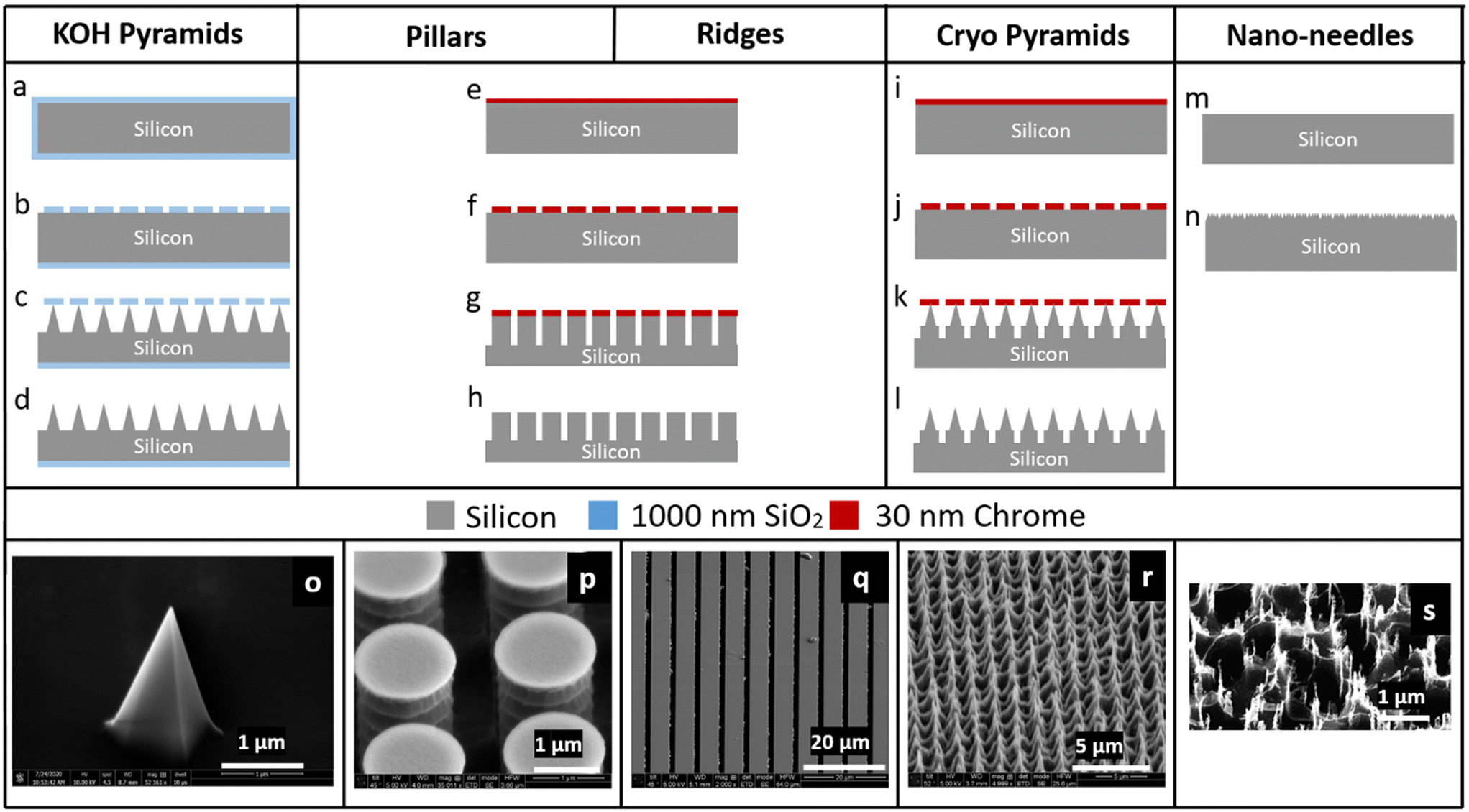 | ||
| Fig. 2 Micropatterned silicon impactor chip fabrication. Process flow to fabricate: (a–d) pointed pyramidal structures, using the KOH-based etching, (e–h) high-density pillars or ridges, using BOSCH etch in DRIE; the same process flow yields two different geometries when using different lithography masks and etch times, (i–l) high-density cryo pyramids, using cryo-etch process, (m and n) nano-needles, using DRIE. SEM images showing (o) a single pyramid fabricated using KOH etching of Si; (p) array of dense cylindrical structures fabricated using BOSCH etch process; (q) array of ridges fabricated using BOSCH etch process; (r) array of dense cryo pyramids using cryo-etch process; (s) array of nano-needles with features of 15–20 nm fabricated using BOSCH etch process. | ||
:propylene glycol methyl ether acetate (PGMEA, Sigma, Cat# 484431) at 2:1 v/v ratio and baked at 115 °C for 1 min (Fig. 2e). The resist was then patterned with either 1.1 μm circles with 0.9 μm gaps, or grids with a width of 5 μm and a gap of 1 μm to generate pillars or ridges, respectively (Fig. S1b and c†). The pattern was developed in 1:4 v/v Developer AZ 351:DI water for 22 s and the residual resist was descummed for 15 s. After this, the wafer was coated with Cr and after lift-off with resist remover 1165 for 6 hours to overnight, the Cr hard mask was obtained (Fig. 2f). This pattern was transferred to the Si wafer by a BOSCH etch process. This process consists of a sequence of repeated alterations between deposition and etch steps with C4F8 and SF6, respectively17 (Fig. 2g). The deposition step was performed at 700 W ICP power, 10 W platen power and with a C4F8/SF6 gas flow of 100 sccm/1 sccm. The etch step was performed at 700 W ICP power, 30 W platen power, with C4F8/SF6 gas flows of 1 sccm/80 sccm. During the deposition and etch steps, the chamber process pressure was 30 mTorr and the electrode temperature was held at 0 °C. To generate pillars (Fig. 2h and p), this process was repeated for 12 cycles; to generate ridges (Fig. 2h and q), this process was repeated for 50 cycles, where one etch step and deposition step together are considered a full cycle.
:PGMEA and baked at 115 °C for 1 min, as described above (Fig. 2i). The resist was patterned (same as Fig. S1b†) and then developed in 1:4 v/v Developer AZ 351:DI water for 22 s. Following descum process for 15 s, the wafer was coated with a Cr hard mask as described above (Fig. 2j). Finally, the pattern was transferred to the Si wafer (Fig. 2k) by a low temperature (−90 °C) cryo-based silicon RIE process,22,23 producing sharpened pyramidal structures (Fig. 2l and r) by lateral undercutting of the Cr mask, with process conditions 700 W ICP power, 3 W platen power, chamber pressure of 5 mTorr, the electrode temperature at −90 °C and with O2 flow of 4.0 sccm, CHF3 flow of 6 sccm, SF6 flow of 32 sccm, and etch rates ∼350 nm min−1.
After each of the five micropatterns were fabricated, the Si wafer quarters were coated in resist S1813 at 1.5 μm thickness and diced into 5 × 5 mm2 chips, using an ADT 7122 dicing tool. Any residual resist was stripped in resist remover 1165, and the chips were rinsed in DI water and dried. At this point, the micropatterned silicon impactor chips were ready to be embedded into the microfluidic device. Overall micropatterned silicon impactor chip fabrication yield was >90% and limited by some sub-optimally developed edge dies along the wafer edge. The features were uniform and of high fidelity. Since the micropatterned silicon impactor chips have fine features, they need to be handled carefully, and held from the sides. It can be helpful to use a vacuum pick-up tool (Pelco, Cat#520-1) to handle these chips.
Soft microfluidic device fabrication and micropatterned silicon impactor chip integration
Assembled devices are composed of a soft microfluidic device made of elastomeric polydimethylsiloxane (PDMS) with a microfluidic channel patterned via soft lithography, a micropatterned silicon impactor chip inset into the soft microfluidic device, a glass substrate, and a metal screw (Fig. 1a).
Fig. 3 illustrates the schematics of the process flow to embed the micropatterned silicon impactor chip into the soft microfluidic device. Devices were designed and assembled using standard soft lithography26 processes. Briefly, a soft microfluidic device was generated by replica molding around a resin mold patterned with the inverse of a microfluidic channel and a square inset of 5 × 5 mm2 for seamless inlay of the microarray-patterned silicon chip. The resin master mold was designed in AutoCAD (AutoDESK, USA) (Fig. S1d†) and printed using a Form 3 3D printer (Formlabs, Somerville, MA) outfitted with V4 Clear Resin (Cat# RS-F2-GPCL-04) set to a process resolution of 25 μm. The printed material was soaked in an IPA tank for 3 hours and UV cured at 75 °C for 7 hours to generate the mold (Fig. 3j) patterned with the inverse of features desired in the final soft microfluidic device, including raised portions which later define the microfluidic channel and an inset for the micropatterned silicon impactor chip. Typical channel dimensions in the soft microfluidic device are 125 μm deep, 1500 μm wide and 58 mm long with a recess of 5000 × 5000 × 450 μm3 halfway between the inlet and outlet, to fit the silicon impactor chip (Fig. 3k and l; CAD file provided as ESI†). Since the thickness of the fabricated silicon chip is ∼503–504 (± 25) μm, there is an overhang of 53–54 μm for the micropatterned silicon impactor chip into the flow channel (Fig. 3i, not drawn to scale), resulting in a channel height of 75 μm under the micropatterned silicon impactor. To cast the mold, PDMS elastomer and cross-linker (Krayden Dow Sylgard 184 Silicone Elastometer Kit) were mixed at a 1:10 w/w ratio using a THINKY AR-100 centrifugal mixer (Laguna Hills, CA) set to 30 s mixing and 30 s degassing, then poured into the resin mold (Fig. 3a and b), degassed gently under vacuum for 20 min to remove air bubbles, and subsequently baked in an oven at 65 °C for >3 hours to cure the PDMS. The cured PDMS was then cut away from the edges of the mold using a scalpel and peeled off, leaving a patterned PDMS block (Fig. 3c). Subsequently, 4 mm sized biopsy punch (Robbins Instruments, Cat# RBP-40) was used to cut a hole at the center of the silicon die inset (Fig. 3d) and a 1 mm biopsy punch (Integra Miltex, Cat# MIL-33-31AA-P/25) was used to cut inlet and outlet holes to the microchannel (Fig. 3e), completing the soft microfluidic device fabrication. The soft microfluidic device was then cleaned by sonication in DI water for 3 min and IPA for 6 min to prepare for incorporation of the micropatterned silicon impactor chip. The micropatterned silicon impactor chip was inlayed and bonded to the elastomer surface of the soft microfluidic device by applying a minute amount of uncured PDMS elastomer and cross-linker mix, prepared as described above, to the PDMS at the corners of the inset and then gently pressing the micropatterned silicon impactor chip, micropatterned side facing outward, into place until flush with the microchannel. The soft microfluidic device and micropatterned silicon impactor chip were then baked, chip-side down, on a 95 °C hotplate for 30 min (Fig. 3f) to cure the fresh PDMS. Following this, the soft microfluidic device with embedded micropatterned silicon impactor chip is ready to be sealed.
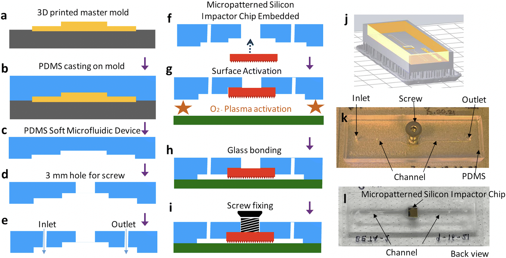 | ||
| Fig. 3 Schematic for device integration. (a) 3D printing the master mold, (b and c) fabrication of soft microfluidic device from master mold, (d and e) punching the 3 mm hole and the fluid inlet/outlets using biopsy punch, (f) embedding micropatterned silicon impactor chip and bonding using uncured PDMS, (g and h) oxygen plasma treatment and bonding of glass slide and soft microfluidic device, (i) inserting a M3 screw and sealing the opening using permanent epoxy, (j) CAD schematic with raft (yellow) and support (gray), (k and l) images of the front and back views of the device showing screw, die and inlet, outlet of the channel. | ||
Glass slides 75 × 38 mm2 (Fisher Scientific, Cat# 12-550B) were cleaned by scrubbing in acetone, then sonicating in acetone for 30 min, IPA (>99.5%) for 10 min, and DI water for 10 min. A 5 × 5 mm2 Si <100> piece was placed over the micropatterned silicon impactor chip to protect its microstructures, while a BD-20AC Laboratory Corona Treater (Electro-Technic Products, USA) was used to apply air plasma alternatingly to the PDMS surface of the soft microfluidic device and the cleaned glass slide for a total of 10 min. After this, the protective Si piece was removed and the treated surfaces were pressed together to create a covalently bonded, leak-proof microfluidic channel. The micropatterned silicon impactor chip remained suspended over the microfluidic channel (Fig. 1a). The device was then baked on a hot plate at 75 °C for 30 min (Fig. 3g and h) to strengthen the covalent bonding between the soft microfluidic device and glass slide. Finally, a M3 screw was inserted into the 3 mm hole behind the micropatterned silicon impactor chip and attached with a small amount of Devcon 2 Ton Epoxy (Fig. 3i), providing a rigid external contact point through which mechanical motion can be transmitted to the embedded chip. The completed device (Fig. 3k and l) is tested for leakage by flowing DI water in the microchannel before it is deemed ready for use.
Cell culture and fluid sample preparation
We performed preliminary impaction tests with porous polystyrene–divinylbenzene beads of 10 μm diameter (Chemgenes) and porous silica (SiO2) beads of 3 μm diameter (Sigma, Cat# 806765). The 10 μm beads came functionalized with hexaethylene glycol and DNA fragments that prevented aggregation. Both 10 μm and 3 μm beads were suspended in DI water at 4.5 million and 65 million beads per mL, respectively. The beads were loaded into syringes (BD biosciences, Cat# 309657) for flow experiments.Next, we used fungal microbes to test lysis from impaction experiments. Two species, Saccharomyces cerevisiae and Candida albicans were tested separately for comparison. S. cerevisiae (strain BY4741, Open Biosystems) and C. albicans (strain SC5314, ATCC) were grown overnight in YEPD medium (MP Biomedicals, Cat# MP114001022) and used in log phase. To prepare the cells for impaction experiments, cells from each species were spun down in a centrifuge at 130 × g for 4 min and the supernatant medium was removed. The cells were washed and spun down at 130 × g for 4 min in 1× PBS (Fisher BioReagents 10× PBS, Cat# BP399500, diluted to 1× using Invitrogen Ultrapure DNase/RNase Free Distilled Water, Cat# 10977023), and re-suspended in 1× PBS. 10 μL of the suspension was removed from the stock and counted on a hemocytometer (InCyto, Cat# DHC-N01-2) and the cell concentration was adjusted to generate 1 mL of cell suspension in 1× PBS at 50 million cells per mL and 400 U mL−1 RNase Inhibitor (Lucigen, Cat# F83923). The cells were stored on ice and loaded into sterile plastic syringes (BD biosciences, Cat# 309657) immediately before use. Effluents were collected on ice to preserve RNA integrity.
Device operation and sample collection
During the device operation, the inlet and outlet channel are used to flow solutions that contain the test specimens (e.g., microbeads or microbes). The micropatterned silicon impactor chip is used as an impactor to mechanically squish or crack the microbeads or microbial cells under flow. When the piezo actuator is activated at an applied frequency and waveform, the micropatterned silicon impactor chip is pushed by the actuator to move up and down continuously such that the microbes or test specimens underneath are squished between the micropattern structures and the glass substrate (Fig. 1a), with the glass substrate acting as an anvil. This piezoelectricity-driven micromechanical actuation of the different fabricated microstructures on the micropatterned silicon impactor chips (pointed pyramids, pillars, ridges, etc.) causes the microbeads or microbial cell walls to either perforate, crack or break due to applied stress, thereby lysing the cell.Vertical motion of the silicon chip was generated using a piezoelectric actuator (P-216.9S piezo actuator model and E-501.00 piezo amplifier/servo controller, Physik Instrumente) (Fig. 1a and b). The piezo actuator has sub-millisecond response time and sub-nanometer resolution but is limited by noise in the amplifier/servo circuitry. A square waveform with peak-to-peak voltage (Vpp) = 10 V, duty cycle = 50%, and frequency = 0.5 Hz was applied to the piezo amplifier using a BK Precision 4053B waveform generator. This translated into a maximum linear displacement of ∼180 μm by the piezoelectric element, which coupled to the micropatterned silicon impactor chip embedded in the fluidic device through the M3 screw (Fig. 1a and 3i and k), resulting in linear displacement of the micropatterned silicon impactor chip into the microfluidic channel and its contents in the same frequency-dependent manner. Any excess piezo motion is accommodated by the flexure in the setup.
Experiments were carried out on a Nikon Epiphot 200 inverted metallurgical microscope, equipped with extra-long working distance 20× and 40× air objectives and a MiChrome 5 Pro (Tucsen) camera to assist with alignment of the piezoelectric element, monitor sample flow through the device and assess micropatterned silicon impactor chip displacement (via change in focal plane). A custom-built rigid baseplate (Fig. 1c) was installed as the sample holder to minimize sag/deformation of the device under mechanical impaction. Likewise, the piezo element was mounted on a mechanically rigid steel gantry (Fig. 1c) to allow the full force of the piezoelectric motion to be transmitted to the micropatterned silicon impactor chip. The gantry design also incorporates a rigid X–Y–Z differential translation stage, consisting of two linear stages (Newport, UMR8.25) with micrometer attachments (Newport, BM17.25) to control horizontal displacements in X and Y with 1 μm sensitivity, and a vertical linear stage (Newport, MVN80) and differential micrometer head (Newport, DM17-25) for Z displacement with 0.1 μm sensitivity. The X–Y–Z translation stage allowed easy alignment of piezo element with the fluidic device while visualizing flow and mechanical impaction.
The micropatterned silicon impactor chip-integrated microfluidic device was placed on the baseplate such that the micropatterned silicon impactor surface could be observed in the microscope's field of view. The sample of interest (either micro-beads or live cells suspended in fluid) was flowed through the device at 300 μL h−1 using a KDS 910 syringe pump (KD Scientific) until the microchannel was completely filled with liquid, displacing any trapped air pockets. Undisturbed flow was maintained for 10 min, discarding the effluent. 50 μL of effluent (without piezo-electrically driven impaction) was collected for ∼10 min as negative control.
Next, the flow was turned off to allow proper alignment of the piezoelectric head. With the optical microscope focused on the bottom of the micropatterned silicon impactor chip, the tip of the piezoelectric head was aligned and brought into contact with the center of the flat top of the M3 screw. Contact was indicated by a slight change in microscope focus corresponding to a small change in the Z-position of the micropatterned silicon impactor chip (depth of focus ∼1 μm). Once contact with the screw's flat top was made, the alignment was fine-tuned to account for any variation of the micropatterned silicon impactor chip in Z-axis. This was done to ensure that the piezo actuation effects crushing (or puncturing) of the payload in the channel (e.g., microbial cells or microbeads ∼1–10 μm in diameter, used as proxy for microbes) when the micropatterned silicon impactor is fully lowered, while the actuation also allows new payload to flow under the silicon chip when it is fully raised. The variation in the Z-location of the micropatterned silicon impactor chip comes from several sources, most notably manufacturer differences in thickness of the silicon wafer (±25 μm), differences between 3D printed molds in the depth of the recess (±10 μm) for the micropatterned silicon impactor chip, and slight differences in the amount of PDMS applied to bond the micropatterned silicon impactor chip to the soft microfluidic device. This final fine tuning and alignment was done by resuming flow through the device with piezo actuation turned on, using the microscope to visualize the movement of the payload between the micropatterned silicon impactor and glass bottom. The Z-position of the piezo head was adjusted until it was observed that new payload flowed underneath the micropatterned silicon impactor when in its fully raised position, and when in its fully lowered position this new payload was not wobbling or moving, indicating that the payload was trapped between the micropatterned silicon impactor and glass slide and thus in contact with both surfaces.
Following alignment, flow was resumed through the device at 300 μL h−1 and piezoelectric actuation in the form of an oscillatory square wave of Vpp = 10 V was applied. After waiting an additional 10 min for residual volume not brought into contact with the actuated micropatterned silicon impactor to flow through and be discarded, 50 μL of the effluent was collected directly into a 200 μL pipette tip with barrier filter (Genesee Scientific, Cat# 24-412) and saved for analysis.
Scanning electron microscopy: sample preparation and imaging
We evaluated the system's ability to mechanically crush microbeads and microbial cells using scanning electron microscopy (SEM). We performed SEM on bead and S. cerevisiae cell residues on the surfaces of micropatterned silicon impactor chips retrieved after the experiments, and also on the effluent fluid collected from the outlet of the fluidic device.Effluent samples of crushed beads were prepared for SEM imaging by placing a small droplet of effluent on a plain Si <100> 5 × 5 mm2 chip and allowing it to dry overnight (or longer). S. cerevisiae effluent samples were prepared for SEM imaging following a modified version of the procedure described in ref. 27. Briefly, glutaraldehyde (GLA; Electron Microscopy Sciences, Cat# 16120) was added to the effluent to a final concentration of 2.5% GLA and the samples were left to fix in a 4 °C fridge for 2 hours. Following fixation, cellular samples were spun down and washed once with 1× PBS at 130 × g for 4 min to remove excess glutaraldehyde and then dehydrated through a series of ethyl alcohol washes at 30%, 50%, 70%, and twice at 100%. A small droplet of the dehydrated sample was placed on a 5 × 5 mm2 piece of plain Si <100> and allowed to dry overnight for SEM imaging.
Samples of crushed microbeads and S. cerevisiae cells on the micropatterned silicon impactor chips were prepared by allowing the device to dry overnight and then extracting the micropatterned silicon impactor chip from the soft microfluidic device using a scalpel. The micropatterned silicon impactor chip was further dried at room temperature overnight. The dried samples were coated with a thin layer of gold (a few nm thick) by sputter coating (Cressington Sputter Coater 108 Auto, Ted Pella, Inc.) for 120 s to enhance contrast under SEM. SEM images were collected using a FEI Nova NanoLab DualBeam focused ion beam (FIB) instrument equipped with high resolution electron beam for SEM.
SEM image analysis to characterize crushed microbeads
The images of effluent samples were sorted according to the size of the microbeads (3, 10 μm) and the type of micropatterned silicon impactor chip used to crush them. Multiple SEM images of 10 μm (acquired at ∼650× magnification) and 3 μm (2000× magnification) microbead samples were used to calculate crushing efficiency.The SEM images were analyzed using the cell counter plugin in NIH ImageJ software. Crushing efficiency for beads was calculated as the number of crushed beads divided by the total number of beads (crushed and uncrushed) in the effluent (Fig. S2l, top†). The number of crushed beads was calculated by estimating the size of visible crushed fragments and multiplying their approximate size by the number of fragments of that size. For simplicity, all visible bead fragments were binned as follows: intact, ½, ¼, ⅛, 1/16, 1/32 and 1/64 times the bead size. Full beads were counted first (e.g., Fig. S2l, bottom, left†), and then crushed bead fragments were counted by their approximate sizes (Fig. S2l, bottom, right†). Intact beads on the borders of the image were included. A tally of the total number of beads versus the number of crushed beads, calculated by multiplying the total count for each size of fragment by the approximate size of the bead fraction and summing the counts from all fractions, was recorded for each micropatterned silicon impactor chip type. The error bars represent the standard error according to data taken from multiple images.
qRT-PCR based quantification of yeast cell lysis on chip
Real-time quantitative reverse transcription-polymerase chain reaction (qRT-PCR) was used to quantify the RNA released into the effluent medium following impaction experiments on S. cerevisiae and C. albicans. qRT-PCR was performed on the effluent lysate at different dilutions, along with positive and negative controls, using the QuantStudio 3 Real-Time PCR, 96-well, 0.2 mL System (Applied Biosystems) and iTaq Universal SYBR Green One-Step Kit (BioRad, Cat# 1725150) with a total reaction volume of 20 μL. All samples and standards had an input volume of 1 μL. PCR primers for S. cerevisiae28 and C. albicans29 were designed and custom-synthesized from IDT (Table S2†).We used qRT-PCR to detect the presence of mRNA for three S. cerevisiae genes: ACT1, UBC6 and TDH3. These genes are good candidates to assess cell lysis due to their high (TDH3, ACT1) or moderate (UBC6) expression levels.28 Crushed cell lysate (indicated as ‘Sample’) was collected as effluent after flowing through the device under piezo actuation and tested at stock concentration and dilutions of 1:10 and 1:100 (denoted as ‘Sample 1:10’ and ‘Sample 1:100’). Effluent of uncrushed S. cerevisiae cells was also collected under flow but with the piezo actuation turned off to be used as a negative control effluent (indicated as ‘N. Control E’). Nuclease-free water was tested as an independent negative control (‘N. Control’). As positive controls (‘P.C.’) for qPCR, we used 50 million S. cerevisiae cells, taken as an aliquot from stock washed with PBS and counted using a hemocytometer as described above, lysed using zymolyase and sarkosyl,30 followed by RNA purification with an extraction column (Zymo Research, Cat# R2070) and elution in 100 μL. Completion of chemical lysis was confirmed visually by the absence of intact cells, using a microscope. Stock solution of P.C., along with dilutions of 10×, 100× and 1000× were used for TDH3, ACT1, and UBC6 in S. cerevisiae experiments.
We also used qRT-PCR to detect mRNA for three C. albicans genes: LSC2, TDH3 and ACT1. TDH3 is one of the highest expressed genes in C. albicans.30 Crushed cells collected as effluent after flowing through the device under piezo actuation were tested at stock concentration (indicated as ‘Sample’) and dilutions of 10× and 100× (denoted as ‘Sample 1:10’ and ‘Sample 1:100’). Uncrushed C. albicans cells were also collected under flow but with the piezo actuation turned off as the negative control effluent (indicated as ‘N. Control E’). As before, we used 50 million C. albicans cells lysed using zymolyase and sarkosyl,30 followed by RNA purification and elution in 100 μL. Stock solution of the lysate denoted as ‘P.C.’, along with dilutions at 5×, 10×, 20× and 100× were used for LSC2, TDH3 and ACT1. PCR amplification experiments were run for 40 cycles, where we see late amplification or no amplification for the N. control. Therefore, the Cq value of the N. control that is extracted is “undetermined”, and this data is not plotted.
Results and discussion
Silicon microarray-patterned chip fabrication
SEM images of the nanofabricated micropatterns show the successful generation of several different types of structures (Fig. 2). KOH pyramids: 2 μm wide, ∼2 μm high, 4–5 μm spacing; pillars: 1.1 μm wide, 5 μm deep, 0.9 μm spacing; ridges: 5 μm wide, 40–50 μm deep, 1 μm spacing; cryo pyramids: 1.5 μm wide, ∼2–3 μm high, 1 μm spacing; nano-needles: 50–200 nm wide, 0.5–1 μm high, 0.3–0.4 μm spacing.Analysis of micro-bead impaction via SEM image analysis
SEM images show the effect of impaction upon the beads using different micropatterned silicon impactor chip types (Fig. 4a–o). We observed bead breakage following impaction in all cases, but the percentage of crushed beads depended on micropatterned silicon impactor chip geometry and the type of beads used. In some cases, we observed instances where the 3 μm beads were perforated by sharp KOH pyramid tips (Fig. 4a). Some beads were also crushed (Fig. S2a†) or ripped away (Fig. S2b†) by the KOH pyramid tips. 3 μm beads were either crushed or embedded in the pillar microarray (Fig. 4d and e and S2c and d†). We also saw cases where the 3 μm porous silica beads distorted the silicon pillars and damaged them. To bypass this, we employed the ridge geometry (Fig. 4g and h), which is mechanically stable and provides improved strength to the micropatterned silicon impactor chip. We also found that fewer beads were crushed when the silicon ridges were perpendicular to the direction of the flow, instead of being aligned with flow (Fig. S2e and f†). When the channels between the ridges are aligned with the flow, the fluid squeezed into the channels by the impaction process can escape forward and backward into the microfluidic channel. When the channel is perpendicular to the flow, this is not possible and a back pressure develops opposing the impaction motion. The ridged micropatterned silicon impactor chips have crushing efficiencies between 10.3–32.8%, depending upon size of the beads.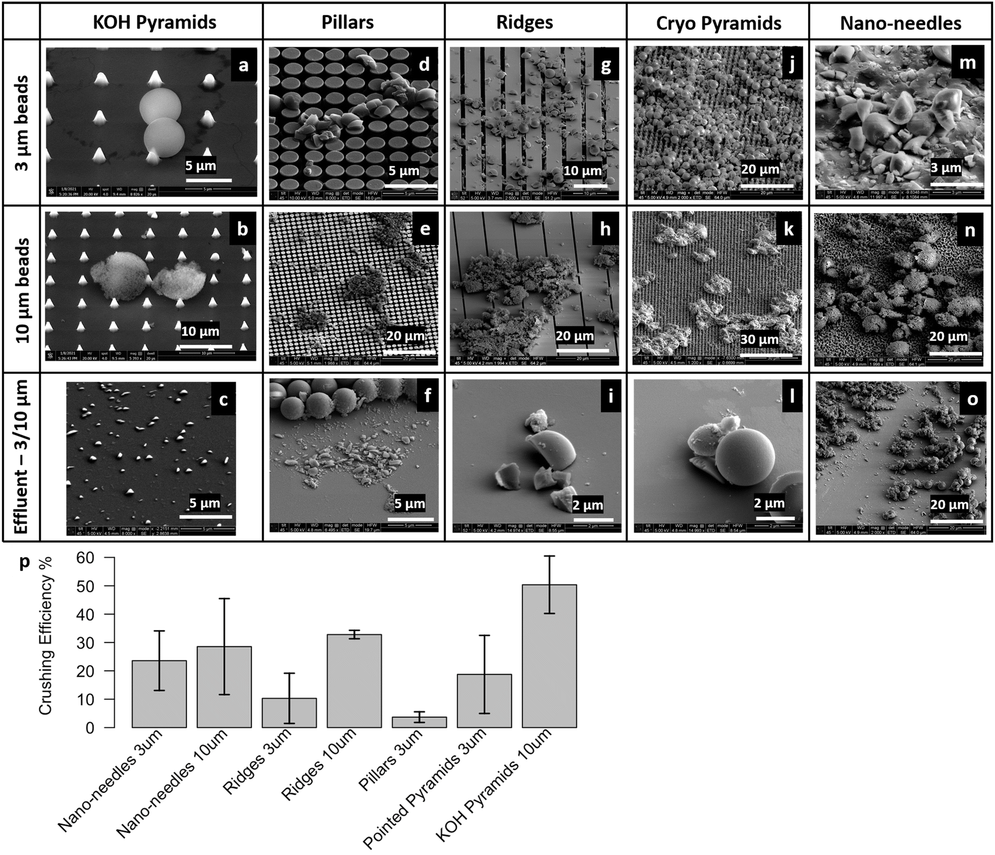 | ||
| Fig. 4 SEM images showing the damage to: (top) 3 μm beads on chip, (middle) 10 μm beads on chip, or (bottom) effluent (3/10 μm beads), caused by micropatterned silicon impactor chip variant (a–c) KOH pyramids, (d–f) pillars, (g–i) ridges, (j–l) cryo pyramids, and (m–o) nano-needles. (p) Bead crushing efficiency reported as the percentage of beads crushed vs. silicon impactor chip type and bead size. Error bars represent standard error in data taken from multiple images. | ||
Detailed analyses of SEM images (described above) of the effluent collected on silicon wafers were performed to estimate the percentage of crushed beads. The crushing efficiencies for different micropatterned silicon impactor chip types and bead sizes are compared (Fig. 4p). Overall, microbead crushing efficiencies varied between 3.7–50.4% for different micropatterned silicon impactor chip geometries. For any given micropatterned silicon impactor chip type, we noted higher crushing efficiency in 10 μm beads compared to 3 μm beads, as the probability of the 10 μm beads escaping between the silicon structures is lower. For example, the spacing between the KOH pyramids is ∼4–5 μm, which the 3 μm beads can escape into, without being crushed. Reducing the gap between the KOH pyramids is difficult due to the crystallographic orientation of silicon used in the etching process. The KOH pyramids showed the maximum crushing efficiency (∼50.4 ± 5.1%) using 10 μm beads.
These results demonstrate that the micropatterned silicon impactor chip travels to within 10–3 μm from the glass substrate with enough force to induce crushing/cracking in the microbeads, and indicate operational success of our piezo-actuated micropatterned silicon impactor designs within the integrated soft microfluidic device environment as proof of concept. A caveat: the crushing efficiency of the black silicon nano-needle chip may be an overestimate because we cannot rule out breakage of the fine black silicon nano-needle structures during piezo-actuated crushing; fragments of black silicon nano-needles in the effluent may distort our estimates of microbead fragments.
In order to examine damage to the silicon micropatterned structures due to impaction, we examined the micropatterned silicon impactor chip surface via SEM following impaction experiments, as well as examined the effluent for chip debris. From these studies we find that the features (see Fig. 4 for nomenclature) on the micropatterned silicon impactor chip with ridges are robust and remain mostly undamaged, occasionally showing some small chips or bowing between ridges. The micropatterned silicon impactor chip type with KOH pyramids is also durable, which remains largely intact after crushing except for some blunting of the pyramid points (Fig. 4a and b) and some pyramids being ripped out (Fig. S2a†), leaving indents behind. The pillars and cryo-pyramids conformations demonstrated less durability, with payload often crushing pillars or cryo-pyramids down, blunting the cryo-pyramids and pushing the pillars apart (Fig. S2c, d, g and h†) and sometimes dislodging the structures in the process. Finally, we found that the nano-needles are most prone to damage, with payload often leaving behind indents on the surface from impaction and flow. Given their scalability and concerns for potential cross-contamination across biological samples, we anticipate they will be single-use, disposable devices.
Device actuation on yeast cells
We also tested micromechanical impaction to crush S. cerevisiae using our setup. S. cerevisiae is a species of yeast commonly used to study fundamental biological mechanisms,31 synthesize biologics32etc. These yeast cells are ellipsoidal33 in shape, typically range from ∼3–6 μm in size34 and have cell walls ranging from 100–200 nm in thickness.34 Even though the KOH pyramids appeared to have highest efficiency in crushing microbeads, we reasoned that the spacing between pyramids is large enough for the S. cerevisiae cells to escape into; hence we chose the second most efficient micropatterned silicon impactor chip, i.e., the ridge geometry for these experiments. We also observed that the ridge geometry is mechanically robust and less prone to damage during fabrication and handling.SEM imaging was performed on cell lysate collected as effluent (Fig. 5a–d). Though S. cerevisiae cells match the porous silica microbeads in size, they do not fragment into multiple pieces, unlike the (more brittle) silica beads. Instead, the cells show a flattened morphology35 with tears on the cell walls (yellow arrow, Fig. 5a and b) or a doughnut morphology (yellow arrow, Fig. 5c and d) after undergoing impaction. S. cerevisiae cells are not amorphous solid spheres like the silica beads, but, with rigid cell walls and aqueous contents, they resemble hollow spheres with rigid shells instead. We posit that, under impaction, S. cerevisiae cell walls may collapse or develop a dent (like a dented ping pong ball), causing the donut morphology.
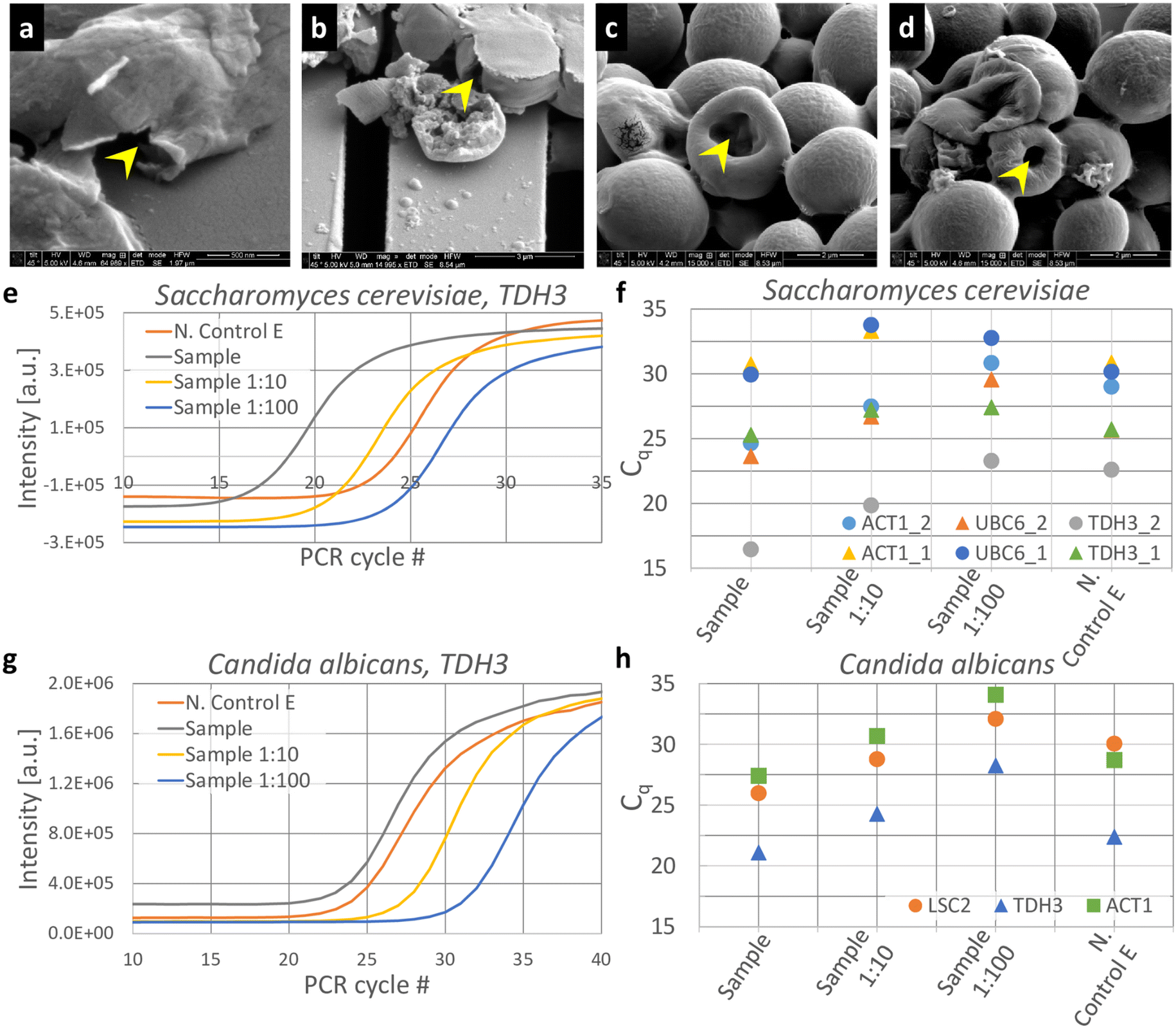 | ||
| Fig. 5 Using the device to crush S. cerevisiae and C. albicans cells for lysis and release of mRNA. (a–d) SEM images of S. cerevisiae crushed using a device with ridged micropattern features. (e–h) qPCR amplification curves for S. cerevisiae and C. albicans lysates collected after the cells were crushed with ridged micropatterned silicon impactor chip. The crushed effluent, ‘Sample’ was tested at stock concentration, 1:10 (‘Sample 1:10’) and 1:100 (‘Sample 1:100’) dilutions. Effluent collected without piezo activity was used as negative control, (‘N. Control E’). mRNA for three commonly expressed genes were tested for each species: (e and f) S. cerevisiae: ACT1, UBC6, TDH3, and (g and h) C. albicans: LSC2, TDH3, ACT1. (f) Cq values extracted from the amplification curves for ACT1, UBC6 and TDH3 mRNA from crushed S. cerevisiae are plotted from 2 different experiments, indicated as ‘_1’ and ‘_2’. (g) PCR amplification curves for crushed C. albicans lysate, ‘Sample’ and dilutions at 10× (‘Sample 1:10’) and 100× (‘Sample 1:100’) are shown, along with uncrushed effluent (N. Control E). (h) Cq values extracted from the amplification curves for LSC2, TDH3 and ACT1 mRNA from crushed C. albicans lysate collected from an impaction experiment are shown for the sample at different dilutions, along with uncrushed effluent. | ||
Fig. 5e shows the PCR amplification curves for ACT1 cDNA in the effluent after impaction activity at stock concentration of S. cerevisiae (marked as ‘Sample’), 10× and 100× dilutions (marked as ‘Sample 1:10’ and ‘Sample 1:100’, respectively), and uncrushed effluent (marked as ‘N. Control E’). Quantification cycle (Cq) values were extracted from the amplification curves for these conditions for ACT1, TDH3 and UBC6 (ref. 28) (Fig. 5f). As the gene with the highest mRNA expression in S. cerevisiae,30 we expect TDH3 to have the lowest Cq value of the three genes tested. The crushed cell samples have Cq values for TDH3 ranging from 16.4 in experiment 1 to 25.3 in experiment 2. We suspect this is due to sedimentation of cells within the device, which could cause slightly different concentrations of cells between experiments. In each case however, the Cq of the crushed sample was lower than the Cq of the corresponding uncrushed sample control. When compared to uncrushed effluent (N. Control E), the crushed cells have a lower mean Cq (ΔCq = 3.3), indicating that the silicon chip impaction indeed caused a fraction of the S. cerevisiae cell walls to lyse and release mRNA into the effluent. This holds for ACT1 and UBC6 also, with mean ΔCq values of 2.2 and 1.1, respectively.
Compared to the S. cerevisiae positive control (P.C.), where 50 million S. cerevisiae cells were lysed and eluted in 100 μL, the crushed effluent has a concentration of 50 million cells per mL. Cq values of S. cerevisiae P.C. at different dilutions are shown in Fig. S3a.† Assuming that the concentration of mRNA in solution is proportional to the number of cells lysed, we posit that if 100% of cells flowed into the device were lysed, the Cq value of the Sample would be comparable to P.C. at 1:10 dilution. A Sample Cq comparable to P.C. at 1:20 dilution would indicate around 50% lysis efficiency, P.C. at 1:100 dilution around 10% lysis efficiency, etc. Sample Cq values of crushed S. cerevisiae lysate typically lay between P.C. 1:100 and P.C. 1:1000, indicating a lysis efficiency of <10%.
Biofouling of the micropatterned silicon impactor chip by crushed cells might potentially decrease lysis efficiency of the device as a function of time. To test if this is the case, we performed lysis experiments on S. cerevisiae cells (under the same conditions as described above), collecting effluent and imaging the micropatterned silicon impactor chip at 5 min, 10 min and 15 min of piezo actuation. Before imaging, the device was flushed with water with the piezo actuation turned off to carry away excess S. cerevisiae that would have been in suspension below the micropatterned silicon impactor chip. After washing, images were taken under 50× magnification at representative points on the chip. After imaging, flow of cells into the device was resumed with the piezo turned off until they were observed to cover the micropatterned silicon impactor chip, at which point piezo actuation was resumed. Piezo actuation on cells under flow was maintained for 5 min. The first 1.5 min of effluent was discarded to eliminate any residual water or uncrushed cells in the device, and then the effluent was collected for 3.5 min for qRT-PCR. If biofouling is indeed an issue, the efficiency of the device would decrease with time, show more cells stuck to the micropatterned silicon impactor chip, and yield lower concentrations of mRNA in the effluent at later time points, requiring higher number of PCR amplification cycles to detect them. As expected, we see a small increase in the number of cells stuck to the micropatterned silicon impactor chip (Fig. S4†), and a small increase in Cq values from the effluents collected at 5 and 15 min time-points [ΔCq = 1.4 (ACT1), 0.8 (UBC6), 0.1 (TDH3) between 5 and 15 min].
We also tested C. albicans cells at 50 million cells per mL for lysis using our setup. As before, qRT-PCR was used to detect the presence of C. albicans mRNA in the crushed lysate that was collected as effluent. Amplification curves for TDH3 cDNA in crushed (‘Sample’) and uncrushed effluents are shown as function of PCR cycles (Fig. 5g), along with 10× and 100× dilutions of the crushed sample. Cq values extracted from the amplification curves of ACT1, LSC2 and TDH3 cDNA (Fig. 5h) show a small but consistent difference in Cq between crushed and uncrushed effluents. TDH3, being one of the top expressed genes in C albicans, is detected at a lower PCR cycle number (21.1) compared to LSC2 and ACT1 (25.9 and 27.4, respectively).
However, the cDNA for these genes are consistently detected at higher PCR cycle numbers compared to S. cerevisiae across multiple experiments (data not shown). C. albicans possess thicker cell walls than S. cerevisiae36 and is therefore more difficult to lyse. We posit that we have a lower efficiency in crushing C. albicans cells on our setup compared to S. cerevisiae, resulting in lower numbers of mRNA in the crushed lysates.
As before, 50 million C. albicans cells were lysed with zymolyase and eluted in 100 μL at stock concentration and serial dilutions were used as positive controls (‘P.C.’) to estimate lysis efficiency of C. albicans cells on our setup (Fig. S3b†). Comparison of Cq values from Sample and P.C. estimates lysis efficiency <10% for C. albicans using our setup.
A factor that influences the crushing efficiency is the “squeeze-flow” configuration of our device, where two parallel surfaces (the micropatterned silicon impactor chip and the glass slide) approach each other under piezo actuation, rapidly pinching off the flow channel in between. As a result, the fluid undergoes acceleration and is ejected out from under the micropatterned silicon impactor chip. If we assume that the payload particles (e.g., microbes) are suspended uniformly in the fluid and get displaced along with the fluid they are suspended in, then the crushing/lysis efficiency is limited by the squeeze-flow configuration, given by efficiency coefficient η = a × d × f/V (i.e., the ratio of the fluid volume impacted by the micropatterned silicon impactor chip per unit time, to the volume that passes under the micropatterned silicon impactor chip per unit time), where a is the footprint of the micropatterned silicon impactor chip, d is the diameter of the payload particles, f is the piezo impaction frequency, and V is the volumetric flow rate. When the micropatterned silicon impactor squeezes down on the payload, we assume that, in the most limiting case, the payload will be displaced along with the fluid, until the micropatterned silicon impactor chip is close enough to the glass substrate that the payload is “stuck” under it, which occurs at a channel gap of ∼d. If we further assume that each impaction results in the entire payload directly under the micropatterned silicon impactor chip getting lysed, then η can provide a very simple estimate of the lysing efficiency. Under our operational conditions, η ∼ 0.3. Note that this estimate is a simple one and does not account for: (i) due to inertia, the velocity of the payload particles will lag that of the surrounding fluid as the fluid accelerates; (ii) following ejection, some of the payload will get drawn back in as a pressure differential arises when the parallel plates open up again, leading to regurgitation. We also anticipate that the payload undergoes impaction several times based on flow rate, micropatterned silicon impactor chip size, separation between the micropatterned silicon impactor chip and glass slide and piezo actuation parameters.
We acknowledge two drawbacks in our experimental setup currently:
In this study, only micropatterned silicon impactor chip types (KOH pyramids, pillars, ridges, cryo pyramids, nano-needles) and payload (beads, cells) were varied, while all other experimental parameters were held constant: flow rate = 300 μL h−1; waveform = square; piezo amplitude = 10 V; piezo frequency = 0.5 Hz; duty cycle = 50% for simplicity and ease of comparison. These experimental parameters were not varied systematically to optimize bead-crushing or cell lysis efficiency. These optimizations are planned for the future.
Summary and conclusions
We present a packaged device and integration technique that incorporates semiconductor-based components like silicon microstructures and functionality into soft microfluidics for the lysis of microbial cells for genomics applications. We describe lithography techniques for fabricating different microstructures on silicon chip, including pyramids, pillars, ridges, dense pointed structures (cryo pyramids) and nano-needles, all of which may be used to break live microbial cell walls through micromechanical impaction to perform cell lysis. In comparing the different micropatterned silicon impactor chip geometries, we find that the ridges are optimal in terms of crushing efficiency and ruggedness. While the cryo pyramids and nano-needles are sharp, they are more fragile and tend to break; the pillars also show occasional damage (as noted earlier). Due to the lateral etching process, the KOH pyramids have a pitch that is too large for cells smaller than 5 μm. We describe the packaging of micropatterned silicon impactor chip into 3D printed soft microfluidic devices and the operation of the integrated device using externally coupled piezo-electric transducer and syringe pump under optical imaging. Synthetic microbeads (polystyrene, silica) of different sizes are tested as proxy for microbial cells of similar shape and size; the microbead fragments are quantified using SEM to estimate crushing efficiency that ranged between 3.7–50.4%, depending on bead size and micropatterned silicon impactor chip geometry. Two microbial species, S. cerevisiae and C. albicans, are tested for lysis by micromechanical impaction using our setup. We used qRT-PCR in addition to SEM to verify lysis of microbial cells using our setup, and estimate lysis <10% for both species.Considering the size of many cells of interest, future experiments will focus on optimizing piezo actuation and flow parameters using micropatterned silicon impactor chips with ridge micropattern geometry. Further, more active or passive components may also be integrated into the system for on-chip characterization of microbial lysate, including imaging, spectroscopy or chemical assays.
Data availability
The data that supports the findings of this study are available within the article and as ESI.†Author contributions
AB and SG conceived the study and planned experiments with PVKN and AK. SG, PVKN, AH, and AB designed and built the setup. PVKN, AH, ERL, SM, RaluD and AB fabricated devices and performed experiments with the help of RD and SG. PVKN, AH, ERL and AB analyzed data. PVKN, AH, SG and AB wrote the manuscript.Conflicts of interest
The authors declare no conflict of interest.Acknowledgements
We thank Dylan Cook for his helpful comments on the manuscript. We thank Christina S. Miller, Liliana Stan and Trevor Wood for help with the dicing saw, e-beam evaporator, sputtering and qRT-PCR help and the CNM Nanofabrication group for providing excellent work conditions in the Clean Room. This work was supported by the University of Chicago BSD FY22 Pilot Projects funding (A. B. & S. G.), NIH DP2AI158157 (A. B.), Vannevar Bush Fellowship (S. G.) under the program sponsored by the Office of the Undersecretary of Defense for Research and Engineering (OUSD (R&E)) and The Office of Naval Research as the executive manager for the grant. ERL was supported by the Quad Undergraduate Research Scholars Program. Worked performed at the Center for Nanoscale Materials, a U.S. Department of Energy Office of Science user facility, was supported by the U.S. DOE, Office of Basic Energy Sciences, under Contract No. DE-AC02-06CH11357.References
- G. M. Whitesides, The origins and the future of microfluidics, Nature, 2006, 442(7101), 368–373, DOI:10.1038/nature05058.
- A. M. Thompson, A. L. Paguirigan, J. E. Kreutz, J. P. Radich and D. T. Chiu, Microfluidics for single-cell genetic analysis, Lab Chip, 2014, 14(17), 3135–3142, 10.1039/c4lc00175c.
- A. Jariani, L. Vermeersch, B. Cerulus, G. Perez-Samper, K. Voordeckers and T. Van Brussel, et al., A new protocol for single-cell RNA-seq reveals stochastic gene expression during lag phase in budding yeast, eLife, 2020, 9, e55320, DOI:10.7554/eLife.55320.
- G. Urbonaite, J. T. H. Lee, P. Liu, G. E. Parada, M. Hemberg and M. Acar, A yeast-optimized single-cell transcriptomics platform elucidates how mycophenolic acid and guanine alter global mRNA levels, Commun. Biol., 2021, 4(1), 822, DOI:10.1038/s42003-021-02320-w.
- M. Shehadul Islam, A. Aryasomayajula and P. R. Selvaganapathy, A Review on Macroscale and Microscale Cell Lysis Methods, Micromachines, 2017, 8(3), 83, DOI:10.3390/mi8030083.
- D. D. Carlo, K.-H. Jeong and L. P. Lee, Reagentless mechanical cell lysis by nanoscale barbs in microchannels for sample preparation, Lab Chip, 2003, 3(4), 287–291, 10.1039/B305162E.
- J. Choi, J.-C. Hyun and S. Yang, On-chip Extraction of Intracellular Molecules in White Blood Cells from Whole Blood, Sci. Rep., 2015, 5(1), 15167, DOI:10.1038/srep15167.
- M. Mahalanabis, H. Al-Muayad, M. D. Kulinski, D. Altman and C. M. Klapperich, Cell lysis and DNA extraction of gram-positive and gram-negative bacteria from whole blood in a disposable microfluidic chip, Lab Chip, 2009, 9(19), 2811–2817, 10.1039/B905065P.
- J. T. Nevill, R. Cooper, M. Dueck, D. N. Breslauer and L. P. Lee, Integrated microfluidic cell culture and lysis on a chip, Lab Chip, 2007, 7(12), 1689–1695, 10.1039/B711874K.
- Y. S. Huh, J. H. Choi, K. A. Huh, T. J. Park, Y. K. Hong and D. H. Kim, et al., Microfluidic cell disruption system employing a magnetically actuated diaphragm, Electrophoresis, 2007, 28(24), 4748–4757, DOI:10.1002/elps.200700366.
- J. Kim, S. Hee Jang, G. Jia, J. V. Zoval, N. A. Da Silva and M. J. Madou, Cell lysis on a microfluidic CD (compact disc), Lab Chip, 2004, 4(5), 516–522, 10.1039/B401106F.
- H. Kido, M. Micic, D. Smith, J. Zoval, J. Norton and M. Madou, A novel, compact disk-like centrifugal microfluidics system for cell lysis and sample homogenization, Colloids Surf., B, 2007, 58(1), 44–51, DOI:10.1016/j.colsurfb.2007.03.015.
- E. Grigorov, B. Kirov, M. B. Marinov and V. Galabov, Review of Microfluidic Methods for Cellular Lysis, Micromachines, 2021, 12(5), 498, DOI:10.3390/mi12050498.
- R. B. Brown and J. Audet, Current techniques for single-cell lysis, J. R. Soc., Interface, 2008, 5(Suppl 2), S131–S138, DOI:10.1098/rsif.2008.0009.focus.
- Y. Huang, E. L. Mather, J. L. Bell and M. Madou, MEMS-based sample preparation for molecular diagnostics, Anal. Bioanal. Chem., 2002, 372(1), 49–65, DOI:10.1007/s00216-001-1191-9.
- K. J. Kobayashi-Kirschvink, S. Gaddam, T. James-Sorenson, E. Grody, J. R. Ounadjela and B. Ge, et al., Raman2RNA: Live-cell label-free prediction of single-cell RNA expression profiles by Raman microscopy, bioRxiv, 2022, preprint, DOI:10.1101/2021.11.30.470655.
- C.-H. Choi and C.-J. Kim, Fabrication of a dense array of tall nanostructures over a large sample area with sidewall profile and tip sharpness control, Nanotechnology, 2006, 17(21), 5326–5333, DOI:10.1088/0957-4484/17/21/007.
- C. Ribbing, B. Cederström and M. Lundqvist, Microfabrication of saw-tooth refractive x-ray lenses in low-Z materials, J. Micromech. Microeng., 2003, 13(5), 714–720, DOI:10.1088/0960-1317/13/5/325.
- H. Seidel, L. Csepregi, A. Heuberger and H. Baumgärtel, Anisotropic Etching of Crystalline Silicon in Alkaline Solutions: I. Orientation Dependence and Behavior of Passivation Layers, J. Electrochem. Soc., 1990, 137(11), 3612–3626, DOI:10.1149/1.2086277.
- J. Belougne, I. Ozerov, C. Caillard, F. Bedu and J. J. Ewbank, Fabrication of sharp silicon arrays to wound Caenorhabditis elegans, Sci. Rep., 2020, 10(1), 3581, DOI:10.1038/s41598-020-60333-7.
- I. Zubel and M. Kramkowska, The effect of isopropyl alcohol on etching rate and roughness of (1 0 0) Si surface etched in KOH and TMAH solutions, Sens. Actuators, A, 2001, 93(2), 138–147, DOI:10.1016/s0924-4247(01)00648-3.
- M. J. Boer, J. G. E. Gardeniers, H. V. Jansen, E. Smulders, M. J. Gilde and G. Roelofs, et al., Guidelines for etching silicon MEMS structures using fluorine high-density plasmas at cryogenic temperatures, J. Microelectromech. Syst., 2002, 11(4), 385–401, DOI:10.1109/JMEMS.2002.800928.
- A. Kamto, R. Divan, A. V. Sumant and S. L. Burkett, Cryogenic inductively coupled plasma etching for fabrication of tapered through-silicon vias, J. Vac. Sci. Technol., A, 2010, 28(4), 719–725, DOI:10.1116/1.3281005.
- M. Michalska, F. Gambacorta, R. Divan, I. S. Aranson, A. Sokolov and P. Noirot, et al., Tuning antimicrobial properties of biomimetic nanopatterned surfaces, Nanoscale, 2018, 10(14), 6639–6650, 10.1039/C8NR00439K.
- E. P. Ivanova, J. Hasan, H. K. Webb, G. Gervinskas, S. Juodkazis and V. K. Truong, et al., Bactericidal activity of black silicon, Nat. Commun., 2013, 4(1), 2838, DOI:10.1038/ncomms3838.
- J. C. McDonald, D. C. Duffy, J. R. Anderson, D. T. Chiu, H. Wu and O. J. Schueller, et al., Fabrication of microfluidic systems in poly(dimethylsiloxane), Electrophoresis, 2000, 21(1), 27–40, DOI:10.1002/(SICI)1522-2683(20000101)21:1<27::AID-ELPS27>3.0.CO;2-C.
- S. A. Shehadat, M. O. Gorduysus, S. S. A. Hamid, N. A. Abdullah, A. R. Samsudin and A. Ahmad, Optimization of scanning electron microscope technique for amniotic membrane investigation: A preliminary study, Eur. J. Dent., 2018, 12(4), 574–578, DOI:10.4103/ejd.ejd_401_17.
- M. A. Teste, M. Duquenne, J. M. Francois and J. L. Parrou, Validation of reference genes for quantitative expression analysis by real-time RT-PCR in Saccharomyces cerevisiae, BMC Mol. Biol., 2009, 10(1471–2199 (Electronic)), 99, DOI:10.1186/1471-2199-10-99.
- H. Nailis, T. Coenye, F. Van Nieuwerburgh, D. Deforce and H. J. Nelis, Development and evaluation of different normalization strategies for gene expression studies in Candida albicans biofilms by real-time PCR, BMC Mol. Biol., 2006, 7(1), 25, DOI:10.1186/1471-2199-7-25.
- R. Dohn, B. Xie, R. Back, A. Selewa, H. Eckart and R. P. Rao, et al., mDrop-Seq: Massively Parallel Single-Cell RNA-Seq of Saccharomyces cerevisiae and Candida albicans, Vaccines, 2022, 10(1) DOI:10.3390/vaccines10010030.
- K. Altmann, M. Dürr and B. Westermann, Saccharomyces cerevisiae as a Model Organism to Study Mitochondrial Biology, in Mitochondria: Practical Protocols, ed. D. Leister and J. M. Herrmann, Humana Press, Totowa, NJ, 2007, pp. 81–90 Search PubMed.
- R. S. Walker and I. S. Pretorius, Applications of Yeast Synthetic Biology Geared Towards the Production of Biopharmaceuticals, Genes, 2018, 9(7), 340, DOI:10.3990/genes9070340.
- T. L. Saito, M. Ohtani, H. Sawai, F. Sano, A. Saka and D. Watanabe, et al., SCMD: Saccharomyces cerevisiae Morphological Database, Nucleic Acids Res., 2004, 32(Database issue), D319–D322, DOI:10.1093/nar/gkh113.
- M. R. Ahmad, M. Nakajima, S. Kojima, M. Homma and T. Fukuda, The effects of cell sizes, environmental conditions, and growth phases on the strength of individual W303 yeast cells inside ESEM, IEEE Trans. Nanobioscience, 2008, 7(3), 185–193, DOI:10.1109/TNB.2008.2002281.
- K. Nowlin, A. Boseman, A. Covell and D. LaJeunesse, Adhesion-dependent rupturing of Saccharomyces cerevisiae on biological antimicrobial nanostructured surfaces, J. R. Soc., Interface, 2015, 12(102), 20140999, DOI:10.1098/rsif.2014.0999.
- F. M. Klis, C. G. de Koster and S. Brul, Cell Wall-Related Bionumbers and Bioestimates of Saccharomyces cerevisiae and Candida albicans, Eukaryotic Cell, 2014, 13(1), 2–9, DOI:10.1128/EC.00250-13.
Footnotes |
| † Electronic supplementary information (ESI) available. See DOI: https://doi.org/10.1039/d2lc00896c |
| ‡ Current Affiliation: Micron Technology, Boise, ID, 83707, USA. |
| § These authors contributed equally. |
| ¶ Current Affiliation: Center for Integrated Nanotechnologies, Los Alamos National Laboratory, Los Alamos, NM 87545, USA. |
| || Present address: Apple Inc., One Apple Park Way, Cupertino, CA 95014, USA. |
| This journal is © The Royal Society of Chemistry 2023 |