
 Open Access Article
 This Open Access Article is licensed under a Creative Commons Attribution-Non Commercial 3.0 Unported Licence
In situ SnSe deposition as passivation for scalable and stable quasi-2D lead–tin perovskite solar cells†
Lijun
Chen
 a,
Eelco Kinsa
Tekelenburg
a,
Kushagra
Gahlot
a,
Matteo
Pitaro
a,
Jun
Xi
b,
Alessia
Lasorsa
a,
Giovanna
Feraco
a,
Loredana
Protesescu
a,
Patrick C. A.
van der Wel
a,
Giuseppe
Portale
a,
Petra
Rudolf
a,
Christoph J.
Brabec
ac and
Maria Antonietta
Loi
*a
a,
Eelco Kinsa
Tekelenburg
a,
Kushagra
Gahlot
a,
Matteo
Pitaro
a,
Jun
Xi
b,
Alessia
Lasorsa
a,
Giovanna
Feraco
a,
Loredana
Protesescu
a,
Patrick C. A.
van der Wel
a,
Giuseppe
Portale
a,
Petra
Rudolf
a,
Christoph J.
Brabec
ac and
Maria Antonietta
Loi
*a
aZernike Institute for Advanced Materials, University of Groningen, Nijenborgh 4, Groningen 9747 AG, The Netherlands. E-mail: M.A.Loi@rug.nl
bKey Laboratory for Physical Electronics and Devices of the Ministry of Education & Shaanxi, Key Lab of Information Photonic Technique, School of Electronic Science and Engineering, Xi’an Jiaotong University, No. 28, Xianning West Road, Xi’an, 710049, China
cInstitute of Materials for Electronics and Energy Technology (i-MEET), Department of Materials Science and Engineering, Friedrich-Alexander-University Erlangen-Nürnberg, Martensstrasse 7, 91058 Erlangen, Germany
First published on 26th September 2023
Abstract
Lead–tin (Pb–Sn) perovskites are a highly promising composition for single-junction and all-perovskite tandem solar cells due to their narrower bandgap and reduced toxicity. While the use of quasi-two-dimensional (quasi-2D) Ruddlesden–Popper phases has resulted in superior stability towards the environment and large improvement in the crystallization with respect to the 3D compositions, very little work has been done towards their deposition with scalable techniques. Here, PEA2(FA0.5MA0.5)4(Pb0.5Sn0.5)5I16 (n = 5) with a gradient structure is successfully prepared for the first time via a two-step blade coating. Perovskite films which are treated with tin(II) acetate (SnAc2) along with N,N-dimethylselenourea (DMS) exhibit a reduced number of surface traps and enhanced surface crystallization, owing to the in situ formation of tin selenide (SnSe). Record devices with power conversion efficiency (PCE) of 15.06%, an open circuit voltage (VOC) of 0.855 V, and negligible hysteresis are obtained. More importantly, the hydrophobic SnSe significantly protects the active layer from the environment. These devices retain 91% of the original PCE after 10 days in ambient air (30–40% humidity) without encapsulation, and almost no degradation of the PCE is detected after over a month of storage in an inert atmosphere, and under continuous MPP tracking for 15 hours.
Broader contextThe road towards commercialization of perovskite solar cells requires efforts towards improving device stability and developing scalable deposition techniques. Lead–tin (Pb–Sn) alloys show great potential for single-junction and all-perovskite tandem solar cells due to their narrower bandgap and reduced toxicity but suffer from inferior stability. Ruddlesden–Popper (RP) perovskites have demonstrated superior stability and enhanced crystallization with respect to 3D compositions. However, quasi-2D RP Pb–Sn devices are rarely reported, especially deposited with scalable techniques, where the state-of-the-art PCE is only about 10%. Here, we demonstrate for the first time a nominal composition PEA2(FA0.5MA0.5)4(Pb0.5Sn0.5)5I16 (n = 5) with a gradient structure deposited by a two-step blade coating. Moreover, a thin passivation layer of SnSe is obtained from the in situ reaction of SnAc2 and DMS on the perovskite surface, which significantly reduces nonradiative recombination and enhanced surface quality. As a result, the output voltage and fill factor of solar cells are significantly improved. In addition, the hydrophobic SnSe also significantly protects the active layer from the environment. This work paves the way for in situ passivation strategies and the development of stable, scalable, and environmentally friendly perovskite devices. |
Introduction
Single-junction Pb-based perovskite solar cells (PSCs) have been extensively investigated in the last few years and recently a certified record PCE of 25.7% was reported.1 However, the road towards commercialization requires efforts towards improving device stability and developing scalable deposition techniques. Mixed Pb–Sn perovskites show a reduced toxicity with respect the pure Pb one,2 but also a narrower bandgap (1.2–1.3 eV). For these reasons, Pb–Sn alloys are one of the ideal candidates as light absorbers, which show great potential not only for single-junction solar cells but also for all-perovskite tandem devices,3,4 as illustrated by the recently reported certified efficiency of 26.4%.5 Lately, a variety of efforts including interface passivation and improved crystallization have been devoted to reducing p-type doping and non-radiative recombination, resulting in record efficiencies (> 23%).6,7 However, Pb–Sn devices are still characterized by inferior stability with respect to the Pb counterpart,8–16 and the environmental sensitivity of Pb–Sn perovskites is considered one of the primary obstacles that limit their further development.17–20One of the most successful strategies to enhance the environmental stability of metal halide perovskites has been the fabrication of quasi-2D systems.21–24 By introducing large organic spacer cations, such as aliphatic or aromatic mono ammonium, diammonium, and triammonium cations,10,25–29 low dimensional systems where layers of inorganic octahedra are separated by the spacer cations are formed. The long organic cations have also been demonstrated to induce preferential crystal orientation by tuning the nucleation,30,31 and lower trap density.32–34 The presence of organic cations on the surface and grain boundaries not only protects the inorganic layers from moisture but also improves their structural stability.35,36 Quasi-2D Ruddlesden–Popper (RP) Pb–Sn perovskites in principle should combine the excellent photovoltaic characteristics of Pb–Sn perovskites with the robust environmental properties of 2D RP systems. However, quasi-2D Pb–Sn perovskite solar cells are rarely reported in the literature, and more related reports are inclined to use a limited amount of long organic cations as nucleation agents. This may be due to the difficulties pertaining to the vertical growth of low-dimensional phases and the competitive crystallization kinetics between Pb and Sn sublattices. The state-of-the-art PCE of quasi-2D Pb–Sn devices is only about 10%,37–39 (see Table 1) but it is interesting to note that these devices show better stability towards the environment compared to 3D counterparts. Therefore, it is important to improve the PCEs of such devices as they may help in obtaining the high stability required for applications.
| Perovskites | V OC (V) | J SC (mA cm−2) | FF (%) | PCE (%) | Fabrication methods | Ref. |
|---|---|---|---|---|---|---|
| (BA)2(MA)3Pb3SnI13 | 0.80 | 12.05 | 61.81 | 5.96 | Spin coating | 37 |
| (BA2MA3Pb4I13)0.6 | 0.808 | 17.39 | 71.24 | 10.013 | Spin coating | 38 |
| (PEA2FA3Sn4I13)0.4 | ||||||
| (t-BA)2(FA0.85Cs0.15)4 | 0.70 | 24.2 | 63 | 10.6 | Spin coating | 39 |
| (Pb0.6Sn0.4)5I16 | ||||||
| PEA2(FA0.5MA0.5)4 | 0.855 | 24.67 | 71 | 15.06 | Blade coating | This work |
| (Pb0.5Sn0.5)5I16 |
Most of the Sn–Pb perovskite solar cells reported up until now were obtained using spin-coating, which is a wasteful technique with precursor utilization rate limited to only 5–10%. This technique, while used in the semiconductor industry at the wafer size, it is not compatible with solar module production. Recently, our group proposed a scalable technique involving a 2D perovskite-template driven growth of 3D Pb–Sn perovskites, where the champion device exhibits a PCE of 9.77% limited by the formation of cracks in the conversion process.40 It is important to note that in this case no special treatments were performed to suppress surface traps, while it is well accepted that surface traps at the interface with electron or hole transport layers play an important role in nonradiative recombination, which affects both device efficiency and stability.41–45
Blade coating is a facile method that has a very high precursor utilization rate and allows tuning of the deposition temperature. Importantly, there are a few industrial-scale techniques which have similar characteristics to those of blade coating, making possible an almost immediate transfer of the deposition conditions. In this work, a quasi-2D Pb–Sn perovskite of PEA2(FA0.5MA0.5)4(Pb0.5Sn0.5)5I16 (PEA = phenethylammonium, FA = formamidinium, MA = methylammonium) with a gradient structure is successfully prepared for the first time using a two-step blade coating process. This technique allows for controlling the growth of perovskite with low temperature manipulation, giving rise to a reference device of a PCE of 12.42%. However, great attention should be given to surface passivation to reduce nonradiative recombination and improve photovoltaic performance. Inspired by the attractive physical properties of SnSe, a surface treatment using SnAc2 + DMS is applied on the quasi-2D perovskite surface. The in situ synthesized SnSe obtained from the reaction of SnAc2 and DMS significantly reduces nonradiative recombination and suppresses ion migration. As a result, we fabricated quasi-2D Pb–Sn perovskite solar cells using a scalable deposition technique, showing a champion PCE of 15.06% and a VOC of 0.855 V. These optimized devices retain 91% of the original PCE after 10 days of storage under ambient conditions (30–40% humidity) without encapsulation and show almost no degradation of the PCE when stored in a glovebox for over 1 month, or under continuous MPP tracking for 15 h. This are highly significant improvements when compared with the stability performance of the reference device without any surface passivation.
Results and discussion
Fig. 1(a) shows the schematic of the two-step blade coating process. In the first step, the inorganic (Pb0.5Sn0.5)I2 film is deposited on the substrate kept at 30 °C, followed by an annealing step at 50 °C. Then, the solution of organic salts including PEAI, FAI, MAI, and MACl are deposited on top to allow their diffusion throughout the inorganic layer of (Pb0.5Sn0.5)I2 to form a quasi-2D Pb–Sn perovskite. Ultraviolet photoelectron spectroscopy (UPS) and UV-vis absorption spectra reveal that we obtained a perovskite with an ideal bandgap (∼1.3 eV) and suitable valence/conduction band (4.31 eV and 5.61 eV), as illustrated in Fig. S1 and S2 (ESI†).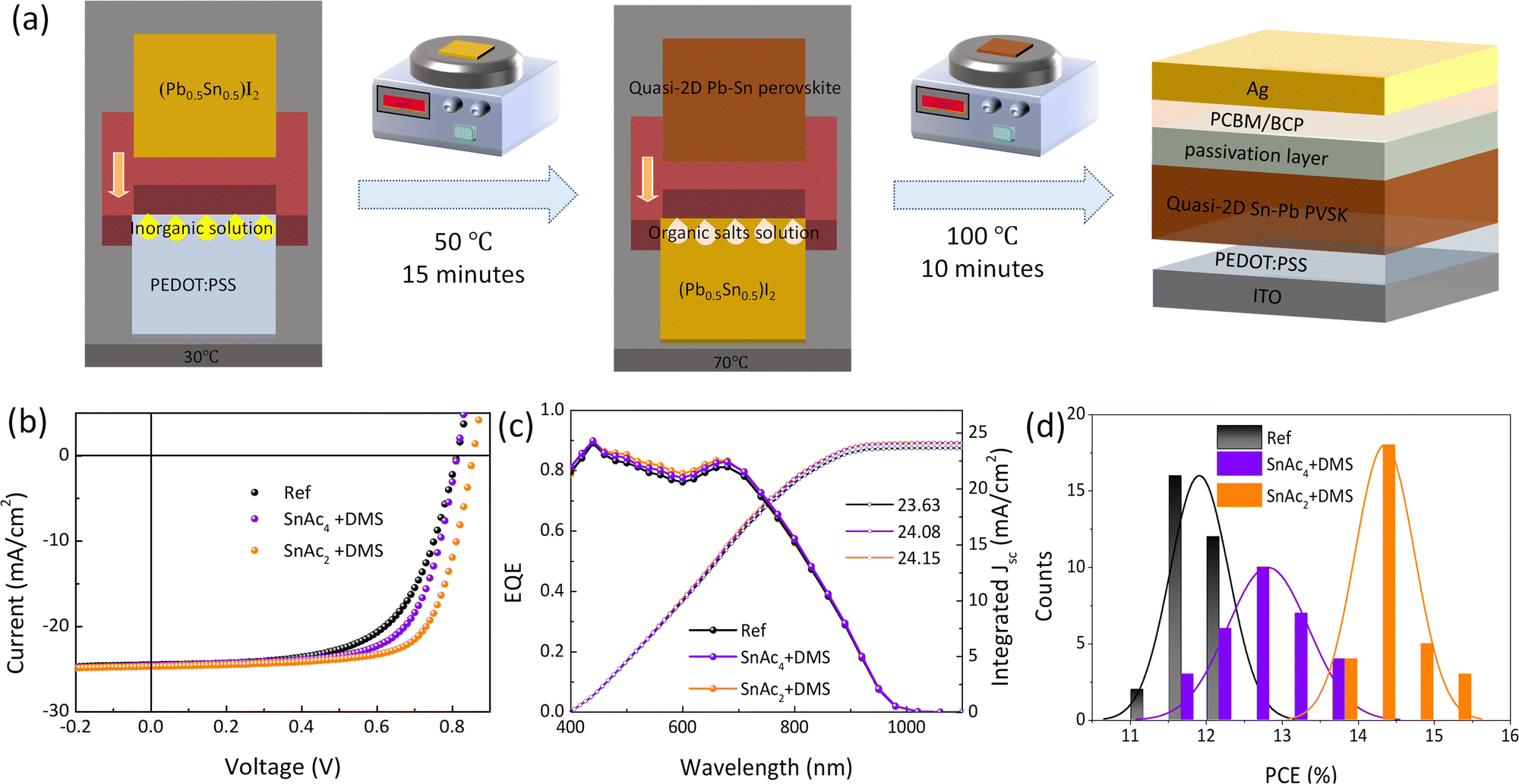 | ||
| Fig. 1 (a) Schematic diagram of the preparation of quasi-2D Pb–Sn perovskite with a two-steps blade coating process. (b) J–V curves of the best-performing PSCs. (c) EQE spectra and integrated photocurrent of the devices. (d) Statistical distribution of PCEs for the three different sample types. | ||
Devices of structure ITO/PEDOT:PSS/Quasi-2D Pb–Sn PVSK/PCBM/BCP/Ag fabricated in this way show a record efficiency of 12.42%, with relatively limited VOC (0.812 V) and FF (62%), as shown in Fig. 1(b). To improve the photovoltaic performances, we investigate the SnAc4 and SnAc2 as possible passivation agents on the perovskite surface, enabling a slight improvement on the VOC and FF (Fig. S3a and Table S1, ESI†). We further investigate the possibility of passivating the surface traps by depositing DMS with SnAc4 and SnAc2, respectively. Interestingly, after surface treatment with SnAc4 + DMS, a higher PCE of 13.65% with an improved FF of 68% is achieved due to the possible passivation provided by carbonyl (C![[double bond, length as m-dash]](https://www.rsc.org/images/entities/char_e001.gif) O) and –NH2 groups. A champion PCE of 15.06% (hysteresis index (HI) of 0.26%) with a much-improved VOC (0.855 V) and FF (71%) is obtained with a SnAc2 + DMS (0.001 M) treatment (Fig. S3b and Table S2, ESI†). We expect that the in situ reaction give rise to the formation of an ultrathin SnSe passivation layer.
O) and –NH2 groups. A champion PCE of 15.06% (hysteresis index (HI) of 0.26%) with a much-improved VOC (0.855 V) and FF (71%) is obtained with a SnAc2 + DMS (0.001 M) treatment (Fig. S3b and Table S2, ESI†). We expect that the in situ reaction give rise to the formation of an ultrathin SnSe passivation layer.
It is important to underline that these devices show excellent area scalability, with devices of 0.81 cm2 exhibiting a PCE of 11.31% (Fig. S3c and Table S3, ESI†), indicating that this strategy is very promising for scalable fabrication of efficient PSCs. Fig. 1(c) shows external quantum efficiency (EQE) spectra with integrated JSC values of 23.63, 24.08, and 24.15 mA cm−2 for the reference and optimized devices, respectively. All values agree well with their corresponding JSC in the J–V characteristics. And we can see an improvement in the EQE spectra after surface passivation in the range between 400 and 700 nm rather than whole wavelength. The minimal inconsistent between UV-vis absorption spectra and EQE is due to differences in the extraction of carriers generated by incident photons of different energy. Fig. 1(d) and Fig. S4 (ESI†) show the results obtained from the characterization of 30 solar cells for each configuration to confirm the reproducibility of the fabrication and surface treatment, the average PCE is improved from 11.91% to 12.81% (SnAc4 + DMS) and 14.33% (SnAc2 + DMS) mainly owing to the large improvement of average VOC and FF.
As mentioned, we propose that the origin of these large improvements in the solar cell performance is the in situ formation of SnSe on the perovskite surface. To prove the formation of SnSe, we conducted control solid state (solvent free) reactions of the precursors at different temperatures (see Fig. S5, ESI†). DMS reacts strongly with the SnAc2 in a solvent free system at a temperature of 60 °C, where the color of the reaction mixture changed from white to black. This is in stark contrast to either SnAc4 or SnI2 solid state reactions with DMS that did not show any variation of color, indicating that the reactivity of SnAc2 with DMS to yield SnSe at low temperature is more favorable compared to the other Sn-based precursors. The reaction scheme for the synthesis of SnSe from SnAc2 and DMS is displayed in the Fig. 2(a). The resulting by-products are volatile at the annealing temperature (acetic acid) or soluble in the solvent used to process the thin-film (acetamide-derivate). For further characterization, we used annealed thin films (80 °C) obtained from precursors dispersed in a mixture of isopropanol (IPA) and chlorobenzene (CB) and solid-state powder reaction (ball-milling). To demonstrate the formation of SnSe from the SnAc2 + DMS and SnAc4 + DMS mixtures, powder X-ray diffraction (XRD) measurements were carried out on the thin films and reported in Fig. 2(b). The fitted diffraction peaks of SnAc2 + DMS are assigned to (201), (111), (311), (411) and (511) planes, (JCPDF 48-1224) corresponding to SnSe orthorhombic (Pnma). The SnAc4 and DMS mixture did not yield any crystalline SnSe product. The formation of SnSe, as well as the mixture of SnAc2 and DMS, was confirmed by the Raman spectra (Fig. 2(c)), where the five vibration modes at 70 cm−1 (Ag1), 102 cm−1 (Bg3), 120–130 cm−1 (board overlapping between Ag1 and Bg1), and 152 cm−1 (Ag3) are present, which is consistent with previously published data.46 The vibrations for the SnAc4 + DMS mixture are very weak, confirming that the formation of SnSe is only favorable from SnAc2, as expected. Interesting, the SnSe powders obtained from solid–solid reaction are not very soluble in a mixture of IPA and CB (1![[thin space (1/6-em)]](https://www.rsc.org/images/entities/char_2009.gif) :1 volume ratio) with a concentration of 1 mM, and when the solution is used as passivation, devices exhibit poor performance with PCE of 10.10% (see Fig. S5b and S5c, ESI†). This results further underline the importance of the in situ deposited SnSe.
:1 volume ratio) with a concentration of 1 mM, and when the solution is used as passivation, devices exhibit poor performance with PCE of 10.10% (see Fig. S5b and S5c, ESI†). This results further underline the importance of the in situ deposited SnSe.
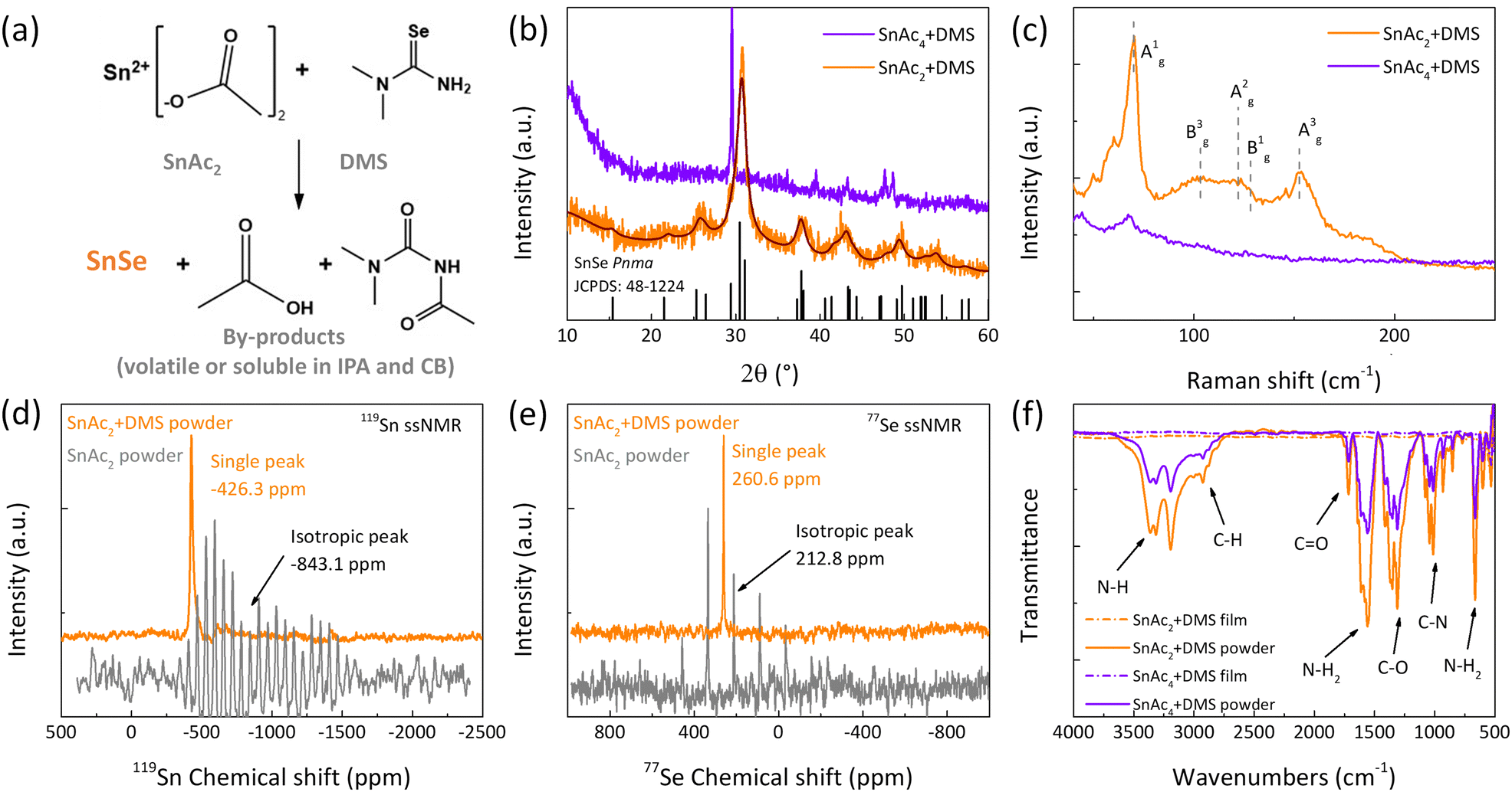 | ||
| Fig. 2 (a) The reaction scheme of SnAc2 and DMS yielding SnSe and by-products (acetic acid and acetamide derivate). (b) Powder XRD patterns of the products between SnAc4, SnAc2 and DMS via thin films procedure after annealing; in black the SnSe Pnma reference is displayed. (c) Raman spectra of the SnAc2 + DMS and SnAc4 + DMS thin films annealed after annealing. (d) 119Sn ssNMR spectra of SnAc2 precursor (gray) and SnAc2 +DMS solid state traction products (orange), showing a change in the isotropic shift (marked with arrows) and MAS side band patterns (see Fig. S6a–d, ESI†). (e) 77Se ssNMR spectra of DMS precursor (gray) and SnAc2 +DMS solid state traction products (orange) (see Fig. S7a and b, ESI†). (f) FTIR spectra of SnAc2 + DMS and SnAc4 + DMS powders, and their corresponding films after thermal annealing. | ||
X-ray photoelectron spectroscopy (XPS) measurements were conducted on the quasi-2D Pb–Sn perovskite films with and without SnAc2 + DMS/SnAc4 + DMS to further elucidate the in situ deposition of SnSe (see details in Fig. S6, ESI†). Moreover, we performed magic-angle-spinning (MAS) solid-state nuclear magnetic resonance (ssNMR) spectroscopy on the solid-state mixture and its precursors (Fig. 2(d), (e) and Fig. S7–S9, ESI†). In the 119Sn ssNMR MAS spectrum, the SnAc2 precursor showed an isotropic peak at −843.1 ppm (gray spectrum, Fig. 2(d)), whereas the SnSe final reaction product displayed an isotropic peak at −426.2 ppm, indicating the complete reaction of SnAc2 even in the solid-state procedure. Fig. S8 (ESI†) shows the 119Sn NMR spectrum from 5000 ppm to −5000 ppm, with no peaks from side products or residual precursors. The 77Se ssNMR spectra (Fig. 2(e)) showed an isotropic peak at 212.8 ppm for the DMS (gray spectrum) and a single peak at 260.6 ppm for the SnSe (orange spectrum). The complete 119Sn and 77Se ssNMR investigation for the precursors and final products are presented in Fig. S7–S9. Both solid-state reactions and the thin films deposition were investigated using Fourier-transform infrared (FTIR) spectroscopy. We noticed that for the solid-state reactions, the vibrations corresponding to the by-products (acetic acid and the acetamide derivate) are present (Fig. 2(f), solid lines), indicated by the functional groups of N–H stretching vibrations (∼3315–3160 cm−1), C–H symmetric stretching vibrations (∼2930 cm−1), CO stretching vibrations (∼1714 cm−1), N–H2 scissoring (∼1555 cm−1), C–O stretching vibrations (∼1310 cm−1), C–N stretching vibrations (∼1014 cm−1), and N–H2 wagging (∼665 cm−1). But when the thin film procedure was performed, no vibration corresponding to the by-products was observed in the mid-IR region. This is due to the solubility and volatility of the by-products, allowing for an efficient solvent and temperature removal from the film surface. SnSe exhibits a suitable band gap (1.3 eV), high absorption coefficient (105 cm−1), and high chemical stability,47 which indicates that it may have broad application prospects in photovoltaic devices. It is important to underline that this passivation strategy based on SnSe is reported here for the first time.
To better understand the impact of the surface treatment on the morphology, scanning electron microscopy (SEM) and atomic force microscopy (AFM) measurements were conducted. As shown in Fig. 3(a)–(c) and Fig. S10 (ESI†), for the SEM and AFM, respectively, the reference sample shows irregularly distributed pinholes and voids, which are known to be accompanied by surface traps.48 The large darker substance appearing in the SEM micrographs corresponds to low-n phases, while the bright signals are attributed to excess PbI2/SnI2. Here, it is important to remember that the sample is fabricated using a two-step process, which easily gives rise to stoichiometric variations along the direction perpendicular to the substrate. For the SnAc4 + DMS treated sample, we observe that the surface is evenly covered with a layer of very small particles, which we expect to originate from the unreacted SnAc4 + DMS. This hypothesis is consistent with the results of both the Raman and XRD measurements. However, the SnAc4 + DMS treated sample shows a dense coverage of the perovskite surface with fewer pinholes and remaining impurities, which seems to be in agreement with the reported device performance improvement. Interestingly the surface treatment performed with SnAc2 + DMS, gives rise to films of uniform surface coverage and densely packed grains without pinholes and voids. Moreover, the reduced amount of the bright signals suggests a possible reduction of the presence of PbI2/SnI2 on the surface, which will be confirmed below by GIWAXS measurements. The AFM images of the three perovskite films present similar surface morphologies to the SEM micrographs (Fig. S10, ESI†).
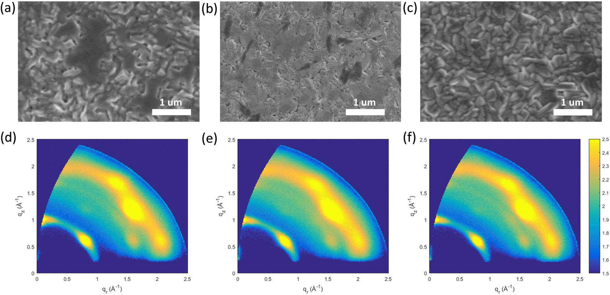 | ||
| Fig. 3 SEM micrographs of the reference perovskite film (a) and of the samples treated with SnAc4 + DMS (b) and SnAc2 + DMS (c). (d)–(f) GIWAXS patterns of the corresponding three different perovskite films recorded using an incident angle of 0.5°. | ||
Grazing-incidence wide-angle X-ray scattering (GIWAXS) measurements are conducted to investigate the film structure and the crystalline orientation in thin films. The GIWAXS patterns were recorded with incident angles of 0.5° (Fig. 3(d)–(f)) and 2° (Fig. S11, ESI†) to probe the structure of the surface and the bulk region of the films, respectively. GIWAXS images taken in the surface region (Fig. 3(d)–(f)) reveal the presence of both low dimensional and 3D-like crystallites. Full peak assignment is reported in Fig. S10 and S12 (ESI†). The GIWAXS peak located at qz ∼ 0.38 nm−1 for the reference film indicates the presence of low dimensional crystallites with n = 3. When the film is treated with SnAc4 + DMS and SnAc2 + DMS, the low dimensional phase is fully transformed to n = 5 (see Fig. S11d, ESI†). In all films, the low dimensional phases are concentrated at the top portion of the perovskite film, indicating that a gradient structure of the quasi-2D perovskite is obtained, which is beneficial to protect it from the interaction with water and oxygen.42 The high angle signals in the GIWAXS patterns can be assigned to the presence of 3D-like crystallites with a cubic structure.49 The 3D-like crystallites present some degree of preferential orientation with crystals oriented both with the (111) and (100) planes parallel to the substrate (Fig. S11, ESI†). In these films produced by the two-step blade-coating procedure the (111) orientation seems to be dominant, in contrast to what previously observed on similar systems produced by a single-step spin-coating method.50 The degree of alignment measurement for the 3D crystals is similar in all the prepared films. In agreement with SEM observations, GIWAXS patterns reveal the presence of highly aligned residual SnI2/PbI2 crystallites for the reference film. Interestingly, when the surface passivation is performed with SnAc4 + DMS, the residual SnI2/PbI2 crystallites diminish sensibly, and they disappear completely when the film is treated with SnAc2 + DMS (see Fig. S10e, ESI†), indicating that the surface treatment is re-crystalizing the top surface of the perovskite. The removal of the SnI2/PbI2 precursor upon surface treatment is also confirmed by XRD (Fig. S13, ESI†), where the increase of the perovskite structural diffraction peaks indicates an enhanced crystallization upon surface treatment. In summary, our combined microscopy and X-ray analysis demonstrates how the two-step blade coating method, followed by a post-deposited chemical passivation allows obtaining dense films of textured 3D-like crystals without residual SnI2/PbI2 crystals, resulting a decrease of the surface traps.
Steady-state photoluminescence (PL) and time-resolved PL (TRPL) are reported in Fig. 4(a) and Fig. S14 (ESI†). The reference sample exhibits lower emission intensity compared to the SnAc2 + DMS sample, implying higher nonradiative recombination associated with traps.51 This is supported by the faster decay dynamics of τavg of 42.47 ns versus 105.69 ns of the reference and SnAc2 + DMS treated samples, respectively (Table S4, ESI†). These observations are well in line with the improvement in VOC observed in devices. We also observe a slight blue shift of the PL peaks from 1.26 eV to 1.30 eV in conjunction with a reduced full width half maximum (FWHM) for the surface treated samples, which could also be attributed to the reduced number of traps states. To better understand the mechanism behind the significant improvement of VOC, a Mott–Schottky plot analysis is conducted and shown in Fig. 4(b). The modified devices exhibit an enhanced built-in potential (Vbi) of 0.81 V (SnAc2 + DMS) and 0.68 V (SnAc4 + DMS) compared to 0.60 V for the reference sample, resulting in an improved VOC.51Fig. 4(c) shows the Nyquist plots of the three devices. The insert is the equivalent circuit for fitting the impedance spectroscopy (EIS) data, which consist of the series resistance (RS), the bulk charge carrier recombination (capacitance C1 and recombination resistance R1), and the interfacial charge recombination (capacitance C2 and recombination resistance R2). A second semicircle is observed at low frequency for the reference and SnAc4 + DMS treated samples. The absence of the second semicircle in SnAc2 + DMS devices demonstrates efficient charge transfer at the perovskite/ETL contact interface after SnAc2 + DMS treatment. Moreover, a much higher recombination resistance is observed for the SnAc2 + DMS treated device compared to the reference and SnAc4 + DMS in EIS measurements, indicating efficient passivation and suppression of carrier recombination with SnSe. The dark J–V curves of the three devices show a similar diode behavior, as shown in Fig. 4(d), but the lowest leakage current density for the SnAc2 + DMS treated sample further indicates that the in situ generated SnSe plays an important role not only in reducing trap-induced recombination but also avoiding leakage. A similar conclusion can be drawn from the space charge limited current (SCLC) investigated with the device structure Au/perovskite/passivation layer/Au.52 As shown in Fig. S15 (ESI†), measurements were conducted at a scan speed of 1 mV s−1 with negligible transient ion diffusion, where the trap-filled limit voltage (VTFL) decreases from 0.60 V for the reference device to 0.53 V and 0.45 V for SnAc4 + DMS and SnAc2 + DMS treated devices, respectively. Therefore, all the experimental evidence shows that the suppressed trap-induced recombination at the contact interlayer with SnAc2 + DMS is at the origin of the high-performance devices.
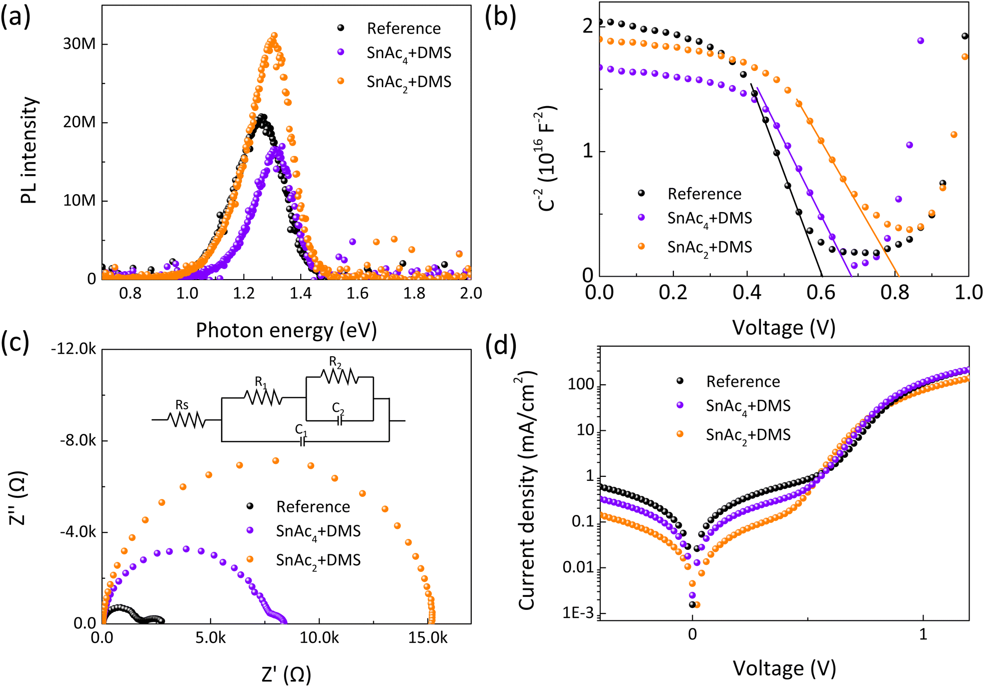 | ||
| Fig. 4 (a) Steady-state PL curves of the reference and optimized perovskite films. (b) Mott–Schottky plots analysis of the devices with and without surface treatment. (c) EIS spectra measured in the dark for the three different samples, the inset shows the equivalent circuit used for the fitting. (d) The dark J–V curves of three corresponding devices. | ||
It has been proposed by many that the surface traps in perovskites easily introduce ion mobility channels, which play a crucial role in device degradation.53 It has also been demonstrated that halide ions migration under an electric field is one of the mechanisms for perovskite memory devices; therefore, we design a resistive random-access memory device to study the trap-induced ion migration behaviors with and without (w/wo) surface treatment.54 Fig. S16 (ESI†) reports the memory device structure of ITO/PEDOT:PSS/Quasi-2D Pb–Sn perovskite/(w/wo) passivation layer/Au, which works by switching the resistance of the perovskites between a high resistance state (HRS) and a low resistance state (LRS). J–V curves are measured at DC voltage (0 → 2 → 0 → −2 → 0 V) with a rate of 0.04 V s−1 under dark condition. As the applied voltage increases from 0 to 2 V, the resistance changes from the HRS to the LRS at a well-defined voltage, as shown in Fig. 5(a)–(c) by the dashed line. This transition voltage represents the barrier for halide ion migration, the large density of traps for the reference device led to a lower transition voltage of 0.94 V compared to 1.02 V of SnAc4 + DMS and 1.18 V for the SnAc2 + DMS treated samples. This memristor behavior represents a further demonstration that the in situ passivation of SnSe plays a vital role in suppressing surface traps.
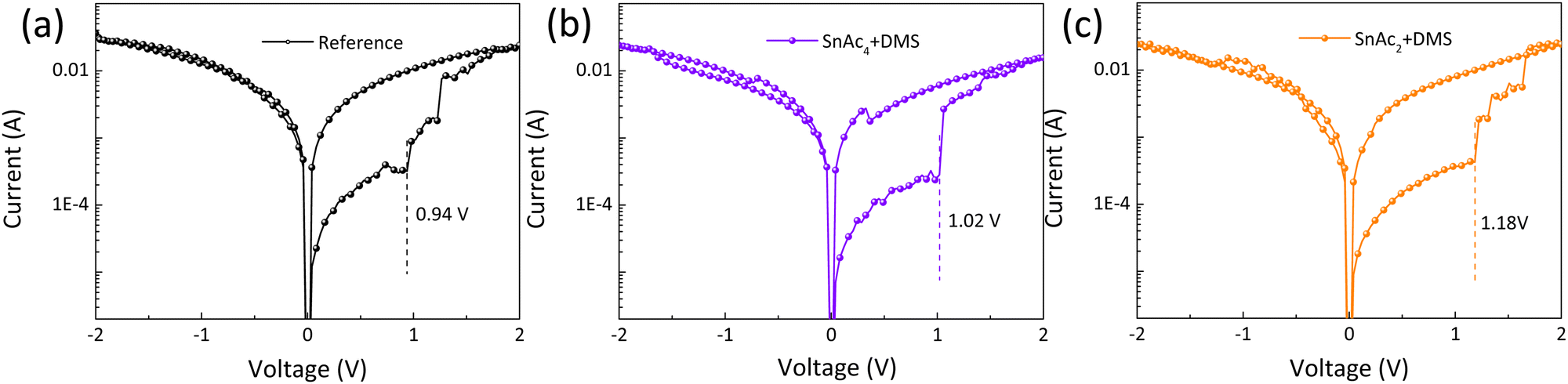 | ||
| Fig. 5 Typical J–V curves of reference (a), SnAc4 + DMS (b), and SnAc2 + DMS (c)-treated memory devices. | ||
The reduced number of surface traps also plays an important role in enhancing the solar cell stability.55 As shown in Fig. 6(a), the non-encapsulation quasi-2D Pb–Sn PSCs with SnAc2 + DMS retain 91% of initial PCE after aging in air (30–40% humidity) for 10 days, while only 55% for reference and 77% for the SnAc4 + DMS sample is maintained under the same conditions. This is further verified by the lower number of pinholes and brighter regions (PbI2/SnI2) after storage in air, as shown by SEM micrographs (Fig. S17, ESI†). The inset shows the contact angle of the three corresponding films, highlighting that the surface treatment with SnAc2 + DMS creates a more hydrophobic surface due to the hydrophobic property of SnSe. Moreover, the non-encapsulated reference PSCs stored for one month in air (humidity 30–40%) clearly shows visible degradation (Fig. S18, ESI†), which is absent for the treated samples. When devices are tested in a N2-filled glovebox, the SnAc2 + DMS treated one shows nearly zero-degradation of the PCE for over one month, while the SnAc4 + DMS and reference samples are degraded by 5% and 25%, respectively (Fig. 6(b)). Naturally, the operational stability under AM 1.5 G standard spectrum is more important for solar cells. As shown in Fig. 6(c), the reference device lost over 50% after MPP tracking for 15 hours owing to light-accelerated ion migration, whereas PSCs with SnAc4 + DMS and SnAc2 + DMS retain 91% and 100% of their initial value, respectively. Therefore, we show that our surface treatment is an effective strategy and promising approach for improving device performance towards industrial standard.
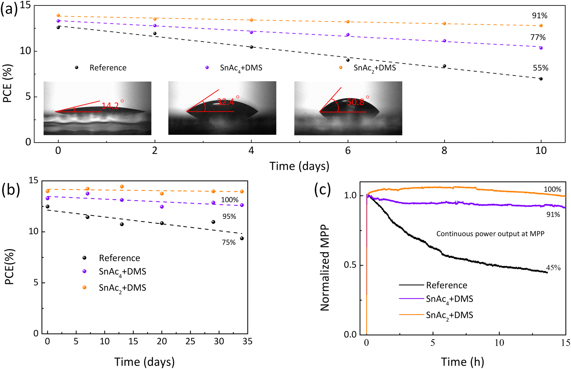 | ||
| Fig. 6 (a) Air stability (30–40% humidity) of non-encapsulated quasi-2D Pb–Sn solar cells, the inset shows the contact angle of three corresponding active layer with passivation. Storage stability (b) and operational stability (c) of non-encapsulated devices in a N2-filled glovebox. The operational stability is measured at the MPP under continuous 1 sun, AM1.5G illumination. | ||
Conclusions
In conclusion, a quasi-2D Pb–Sn perovskite of composition PEA2(FA0.5MA0.5)4(Pb0.5Sn0.5)5I16 with a gradient structure has for the first time been successfully prepared via a two-step blade coating. An in situ reaction method is proposed to further reduce the number of surface traps. We compared two different surface treatments utilizing SnAc2 + DMS and SnAc4 + DMS, and we demonstrate the in situ synthesis of SnSe on the perovskite surface by using SnAc2 + DMS. The sample with SnSe exhibits a reduced trap density and decreased nonradiative recombination losses. Therefore, we obtain a record PCE of 15.06% with a VOC of 0.855 V, which are very significant improvements respect to the reference device (PCE of 12.42%, VOC of 0.812 V) and the sample using SnAc4 + DMS (PCE of 13.65%, VOC of 0.812 V) for which SnSe formation is not observed. It is important to stress that the hydrophobic SnSe significantly reduces the interaction with ambient gases. Therefore, the PSCs treated with SnAc2 + DMS showed remarkable environmental stability and operational stability, retaining 91% of the initial PCE after 10 days in ambient air (30–40% humidity) without encapsulation, and showing almost no degradation of the PCE for both storage in a glovebox over one month and under continuous MPP tracking for 15 h. We believe these results pave the way for the development of stable and environmentally friendly perovskite devices.Author contributions
L. Chen was responsible for device fabrication and measurement as well as the writing of the manuscript. E. K. Tekelenburg helped the Raman measurements as well as the PL studies. K. Gahlot, A. Lasorsa, L. Protesescu, and P. C. A. van der Wel conducted the NMR experiments and analysed the data. M. Pitaro assisted with SEM measurements. K. Gahlot and L. Protesescu also assisted with the FTIR experiments and helped edit the manuscript. J. Xi measured and helped interpret the UPS data. G. Portale helped measure and analyze the GIWAXS data. C. J. Brabec helped improve data analysis of the entire manuscript. Giovanna Feraco and Petra Rudolf conducted the XPS measurement and analysis. M. A. Loi supervised the project, assisted with the writing of the manuscript. All authors commented on the manuscript.Conflicts of interest
There are no conflicts to declare.Acknowledgements
The authors are thankful for the kind technical support of Arjen Kamp, Teo Zaharia, and Lorenzo Di Mario. L. Chen acknowledges the China Scholarship Council. This publication is part of the Netherlands Organization of Scientific Research (NWO) – Focus Group “Next Generation Organic Photovoltaics”, participating in the Dutch Institute for Fundamental Energy Research (DIFFER) and CogniGron research center. This work was partially funded by the European Union's Horizon 2020 program, through a FET Proactive research and innovation action under grant agreement No. 101084124 (DIAMOND). J. Xi acknowledges the National Natural Science Foundation of China (Grant No. 62205264), and Xi'an Jiaotong University Young Talents Support Program (11302291010704).References
- O. Almora, D. Baran, G. C. Bazan, C. Berger, C. I. Cabrera, K. R. Catchpole, S. Erten-Ela, F. Guo, J. Hauch, A. W. Y. Ho-Baillie, T. J. Jacobsson, R. A. J. Janssen, T. Kirchartz, N. Kopidakis, Y. Li, M. A. Loi, R. R. Lunt, X. Mathew, M. D. McGehee, J. Min, D. B. Mitzi, M. K. Nazeeruddin, J. Nelson, A. F. Nogueira, U. W. Paetzold, N. G. Park, B. P. Rand, U. Rau, H. J. Snaith, E. Unger, L. Vaillant-Roca, H. L. Yip and C. J. Brabec, Adv. Energy Mater., 2021, 11, 2102526 CrossRef CAS.
- L. Xiao, T. An, C. Deng, X. Xu and H. Sun, Energy Environ. Sci., 2023, 16, 2120–2132 RSC.
- D. Zhao, Y. Yu, C. Wang, W. Liao, N. Shrestha, C. R. Grice, A. J. Cimaroli, L. Guan, R. J. Ellingson, K. Zhu, X. Zhao, R.-G. Xiong and Y. Yan, Nat. Energy, 2017, 2, 17018 CrossRef CAS.
- M. T. Klug, R. L. Milot, J. B. Patel, T. Green, H. C. Sansom, M. D. Farrar, A. J. Ramadan, S. Martani, Z. Wang, B. Wenger, J. M. Ball, L. Langshaw, A. Petrozza, M. B. Johnston, L. M. Herz and H. J. Snaith, Energy Environ. Sci., 2020, 13, 1776–1787 RSC.
- R. Lin, J. Xu, M. Wei, Y. Wang, Z. Qin, Z. Liu, J. Wu, K. Xiao, B. Chen, S. M. Park, G. Chen, H. R. Atapattu, K. R. Graham, J. Xu, J. Zhu, L. Li, C. Zhang, E. H. Sargent and H. Tan, Nature, 2022, 603, 73–78 CrossRef CAS.
- J. Wang, M. A. Uddin, B. Chen, X. Ying, Z. Ni, Y. Zhou, M. Li, M. Wang, Z. Yu and J. Huang, Adv. Energy Mater., 2023, 13, 2204115 CrossRef CAS.
- G. Kapil, T. Bessho, Y. Sanehira, S. R. Sahamir, M. Chen, A. K. Baranwal, D. Liu, Y. Sono, D. Hirotani, D. Nomura, K. Nishimura, M. A. Kamarudin, Q. Shen, H. Segawa and S. Hayase, ACS Energy Lett., 2022, 7, 966–974 CrossRef CAS.
- J. Cao, H. L. Loi, Y. Xu, X. Guo, N. Wang, C. K. Liu, T. Wang, H. Cheng, Y. Zhu, M. G. Li, W. Y. Wong and F. Yan, Adv. Mater., 2022, 34, e2107729 CrossRef PubMed.
- H. Liu, L. Wang, R. Li, B. Shi, P. Wang, Y. Zhao and X. Zhang, ACS Energy Lett., 2021, 6, 2907–2916 CrossRef CAS.
- S. Shao and M. A. Loi, Adv. Energy Mater., 2021, 11, 2003907 CrossRef CAS.
- M. Pitaro, E. K. Tekelenburg, S. Shao and M. A. Loi, Adv. Mater., 2022, 34, e2105844 CrossRef PubMed.
- H. Kim, J. W. Lee, G. R. Han, S. K. Kim and J. H. Oh, Adv. Funct. Mater., 2020, 31, 2008801 CrossRef.
- C. Li, R. Ma, X. He, T. Yang, Z. Zhou, S. Yang, Y. Liang, X. W. Sun, J. Wang, Y. Yan and W. C. H. Choy, Adv. Energy Mater., 2020, 10, 1903013 CrossRef CAS.
- J. Werner, T. Moot, T. A. Gossett, I. E. Gould, A. F. Palmstrom, E. J. Wolf, C. C. Boyd, M. F. A. M. van Hest, J. M. Luther, J. J. Berry and M. D. McGehee, ACS Energy Lett., 2020, 5, 1215–1223 CrossRef CAS.
- T. Jiang, Z. Chen, X. Chen, X. Chen, X. Xu, T. Liu, L. Bai, D. Yang, D. Di, W. E. I. Sha, H. Zhu and Y. M. Yang, ACS Energy Lett., 2019, 4, 1784–1790 CrossRef CAS.
- C. Li, Y. Pan, J. Hu, S. Qiu, C. Zhang, Y. Yang, S. Chen, X. Liu, C. J. Brabec, M. K. Nazeeruddin, Y. Mai and F. Guo, ACS Energy Lett., 2020, 5, 1386–1395 CrossRef CAS.
- W. Ke, C. Chen, I. Spanopoulos, L. Mao, I. Hadar, X. Li, J. M. Hoffman, Z. Song, Y. Yan and M. G. Kanatzidis, J. Am. Chem. Soc., 2020, 142, 15049–15057 CrossRef CAS PubMed.
- J. Wang, K. Datta, J. Li, M. A. Verheijen, D. Zhang, M. M. Wienk and R. A. J. Janssen, Adv. Energy Mater., 2020, 10, 2000566 CrossRef CAS.
- S. Hu, K. Otsuka, R. Murdey, T. Nakamura, M. A. Truong, T. Yamada, T. Handa, K. Matsuda, K. Nakano, A. Sato, K. Marumoto, K. Tajima, Y. Kanemitsu and A. Wakamiya, Energy Environ. Sci., 2022, 15, 2096 RSC.
- R. Prasanna, T. Leijtens, S. P. Dunfield, J. A. Raiford, E. J. Wolf, S. A. Swifter, J. Werner, G. E. Eperon, C. de Paula, A. F. Palmstrom, C. C. Boyd, M. F. A. M. van Hest, S. F. Bent, G. Teeter, J. J. Berry and M. D. McGehee, Nat. Energy, 2019, 4, 939–947 CrossRef CAS.
- C. Katan, N. Mercier and J. Even, Chem. Rev., 2019, 119, 3140–3192 CrossRef CAS.
- S. Shao, J. Liu, G. Portale, H.-H. Fang, G. R. Blake, G. H. ten Brink, L. J. A. Koster and M. A. Loi, Adv. Energy Mater., 2018, 8, 1702019 CrossRef.
- H. Ren, S. Yu, L. Chao, Y. Xia, Y. Sun, S. Zuo, F. Li, T. Niu, Y. Yang, H. Ju, B. Li, H. Du, X. Gao, J. Zhang, J. Wang, L. Zhang, Y. Chen and W. Huang, Nat. Photonics, 2020, 14, 154–163 CrossRef CAS.
- J. Dong, S. Shao, S. Kahmann, A. J. Rommens, D. Hermida-Merino, G. H. ten Brink, M. A. Loi and G. Portale, Adv. Funct. Mater., 2020, 30, 2001294 CrossRef CAS.
- H. Lai, D. Lu, Z. Xu, N. Zheng, Z. Xie and Y. Liu, Adv. Mater., 2020, 32, e2001470 CrossRef PubMed.
- W. Fu, H. Liu, X. Shi, L. Zuo, X. Li and A. K. Y. Jen, Adv. Funct. Mater., 2019, 29, 1900221 CrossRef.
- N. Zhou, Y. Shen, L. Li, S. Tan, N. Liu, G. Zheng, Q. Chen and H. Zhou, J. Am. Chem. Soc., 2018, 140, 459–465 CrossRef CAS PubMed.
- J. Xi, I. Spanopoulos, K. Bang, J. Xu, H. Dong, Y. Yang, C. D. Malliakas, J. M. Hoffman, M. G. Kanatzidis and Z. Wu, J. Am. Chem. Soc., 2020, 142, 19705–19714 CrossRef CAS PubMed.
- X. Li, K. Li, B. Wang, X. Zhang, S. Yue, Y. Li, Q. Chen, S. Li, T. Yue, H. Zhou and Y. Zhang, Adv. Funct. Mater., 2021, 31, 2107675 CrossRef CAS.
- J. Liang, Z. Zhang, Q. Xue, Y. Zheng, X. Wu, Y. Huang, X. Wang, C. Qin, Z. Chen and C.-C. Chen, Energy Environ. Sci., 2022, 15, 296–310 RSC.
- J. Zhang, J. Qin, M. Wang, Y. Bai, H. Zou, J. K. Keum, R. Tao, H. Xu, H. Yu, S. Haacke and B. Hu, Joule, 2019, 3, 3061–3071 CrossRef CAS.
- X. Lian, H. Wu, L. Zuo, G. Zhou, X. Wen, Y. Zhang, G. Wu, Z. Xie, H. Zhu and H. Chen, Adv. Funct. Mater., 2020, 30, 2004188 CrossRef CAS.
- Z. Wang, Q. Wei, X. Liu, L. Liu, X. Tang, J. Guo, S. Ren, G. Xing, D. Zhao and Y. Zheng, Adv. Funct. Mater., 2020, 31, 2008404 CrossRef.
- Y. Huang, Y. Li, E. L. Lim, T. Kong, Y. Zhang, J. Song, A. Hagfeldt and D. Bi, J. Am. Chem. Soc., 2021, 143, 3911–3917 CrossRef CAS.
- P. Liu, N. Han, W. Wang, R. Ran, W. Zhou and Z. Shao, Adv. Mater., 2021, 33, e2002582 CrossRef.
- Y. Zhang and N.-G. Park, ACS Energy Lett., 2022, 7, 757–765 CrossRef CAS.
- Y. Chen, Y. Sun, J. Peng, P. Chabera, A. Honarfar, K. Zheng and Z. Liang, ACS Appl. Mater. Interfaces, 2018, 10, 21343–21348 CrossRef CAS PubMed.
- Y. Wang, X. Lin, R. Zhou, T. Chen, Q. Lou, Q. Li and H. Zhou, Adv. Photonics Res., 2022, 3, 2200079 CrossRef CAS.
- D. Ramirez, K. Schutt, Z. Wang, A. J. Pearson, E. Ruggeri, H. J. Snaith, S. D. Stranks and F. Jaramillo, ACS Energy Lett., 2018, 3, 2246–2251 CrossRef CAS.
- J. Xi, H. Duim, M. Pitaro, K. Gahlot, J. Dong, G. Portale and M. A. Loi, Adv. Funct. Mater., 2021, 31, 2105734 CrossRef CAS.
- X. Li, W. Zhang, X. Guo, C. Lu, J. Wei and J. Fang, Science, 2022, 375, 434 CrossRef CAS.
- J. Lu, T. Yang, T. Niu, N. Bu, Y. Zhang, S. Wang, J. Fang, X. Chang, T. Luo, J. Wen, Y. Yang, Z. Ding, K. Zhao and S. Liu, Energy Environ. Sci., 2022, 15, 1144–1155 RSC.
- B. Li, H. Di, B. Chang, R. Yin, L. Fu, Y. N. Zhang and L. Yin, Adv. Funct. Mater., 2021, 31, 2007447 CrossRef CAS.
- Y. Su, J. Yang, G. Liu, W. Sheng, J. Zhang, Y. Zhong, L. Tan and Y. Chen, Adv. Funct. Mater., 2021, 32, 2109631 CrossRef.
- S. Yu, M. Abdellah, T. Pullerits, K. Zheng and Z. Liang, Adv. Funct. Mater., 2021, 31, 2104342 CrossRef CAS.
- J. Zhang, H. Zhu, X. Wu, H. Cui, D. Li, J. Jiang, C. Gao, Q. Wang and Q. Cui, Nanoscale, 2015, 7, 10807–10816 RSC.
- V. R. Minnam Reddy, S. Gedi, B. Pejjai and C. Park, J. Mater. Sci.: Mater. Electron., 2016, 27, 5491–5508 CrossRef CAS.
- S. Shao, M. Abdu-Aguye, T. S. Sherkar, H.-H. Fang, S. Adjokatse, G. T. Brink, B. J. Kooi, L. J. A. Koster and M. A. Loi, Adv. Funct. Mater., 2016, 26, 8094–8102 CrossRef CAS.
- S. Kahmann, Z. Chen, O. Hordiichuk, O. Nazarenko, S. Shao, M. V. Kovalenko, G. R. Blake, S. Tao and M. A. Loi, ACS Appl. Mater. Interfaces, 2022, 14, 34253–34261 CrossRef CAS PubMed.
- M. Pitaro, R. Pau, H. Duim, M. Mertens, W. T. M. Van Gompel, G. Portale, L. Lutsen and M. A. Loi, Appl. Phys. Rev., 2022, 9, 021407 CAS.
- S. Shao, Y. Cui, H. Duim, X. Qiu, J. Dong, G. H. Ten Brink, G. Portale, R. C. Chiechi, S. Zhang, J. Hou and M. A. Loi, Adv. Mater., 2018, 30, e1803703 CrossRef PubMed.
- L. Chen, Z. Yin, S. Mei, X. Xiao and H.-Q. Wang, J. Power Sources, 2021, 499, 229909 CrossRef CAS.
- D. Meggiolaro, E. Mosconi and F. De Angelis, ACS Energy Lett., 2019, 4, 779–785 CrossRef CAS.
- Y. Shao, Y. Fang, T. Li, Q. Wang, Q. Dong, Y. Deng, Y. Yuan, H. Wei, M. Wang, A. Gruverman, J. Shield and J. Huang, Energy Environ. Sci., 2016, 9, 1752–1759 RSC.
- S. Yang, S. Chen, E. Mosconi, Y. Fang, X. Xiao, C. Wang, Y. Zhou, Z. Yu, J. Zhao, Y. Gao, F. D. Angelis and J. Huang, Science, 2019, 365, 473–478 CrossRef CAS PubMed .1.
Footnote |
| † Electronic supplementary information (ESI) available. See DOI: https://doi.org/10.1039/d3ee02507a |
| This journal is © The Royal Society of Chemistry 2023 |