
 Open Access Article
 This Open Access Article is licensed under a
 Creative Commons Attribution 3.0 Unported Licence
Perovskite ionics – elucidating degradation mechanisms in perovskite solar cells via device modelling and iodine chemistry†
Sapir
Bitton
 and
Nir
Tessler
*
and
Nir
Tessler
*
Sara and Moshe Zisapel Nano-electronic Center, Electrical and Computer Electronics, Technion Israel Institute of Technology, Haifa, Israel. E-mail: nir@technion.ac.il
First published on 11th May 2023
Abstract
We study recombination pathways in halide perovskite solar cells using a semiconductor device model that includes iodide diffusion and iodide reactions. We stress the device at a bias of 0.9 V, close to the maximum power point, and compare blocking layers impermeable to ions and those that allow ionic transport. For both cases, we examine the impact of incorporating iodide reactions. By comparing stress under dark and one sun excitation conditions, we find that the photoexcited charges enable the redistribution of iodide, which in the case of permeable blocking layers results in the deterioration of the power conversion efficiency and the appearance of hysteresis. If all the reactions are reversible and there is no loss of iodine, their main effect is the introduction of mobile recombination centres. Introducing reactive electrodes that react with and immobilise the iodide results in a rapid loss of performance on the time scale of an hour, which is only slightly accelerated under illumination. We also find that under light excitation, there is a generation of iodine molecules (I2). If the I2 is allowed to leave the device, this constitutes a slow (1000s of hours), but non-reversible degradation pathway. Encouragingly, a judicial choice of the electron-blocking layer's energy levels could suppress this degradation path.
Broader contextThe efficiency of perovskite solar cells marks them as a promising technology. However, this is still challenged by the cells’ stability. In this paper, we present, for the first time, an extended device model that can account for the cell's degradation mechanisms and explore their kinetics. We account for iodide diffusion across the entire device and include iodine reactions that result in (I−, I0, I2). We show that this model can reproduce known phenomena while providing a new mechanism for their activation. For example, iodine redistribution under light excitation is believed to be associated with hole trapping that releases I0 from the perovskite crystal. We show that in a system like a perovskite, where the density of iodine is high enough that, at room temperature, there will be an equilibrium density of interstitial iodide, there is a device-level explanation for the same phenomena. Namely, optically injected electrons electrostatically release the iodide from its positive vacancy. We also show where the iodine molecule is being generated (EBL) and suggest a way to mitigate this potentially irreversible loss of iodine (I2 gas leaking out). The destructive effect of reactive contacts is also demonstrated and is placed in the context of the other effects. |
Introduction
Metal halide perovskite is a class of semiconducting materials with remarkable light-absorption coefficients1,2 and high defect tolerance.3,4 Therefore, perovskites are being widely investigated in several device architectures, such as photodetectors, light-emitting diodes, memristors, and lasers, but mainly solar cells.5,6 In the past decade, perovskite solar cells’ power conversion efficiency (PCE) has rapidly risen to above 25%.7 However, their low environmental stability hinders their integration into industrial applications. For example, halide perovskites suffer from instabilities induced by external factors such as oxygen8 and moisture,9 and intrinsic instabilities, even when not exposed to environmental conditions.10 Moreover, the perovskite solar cells’ degradation increases under the device operating conditions of light,11 heating,12 and bias voltage.13In the following, we review some of the properties of perovskite materials and devices where part of the motivation is to justify our modelling approach. It should be noted upfront that the semiconductor device model framework cannot capture rich chemical physics. We can only hope for it to be good enough to advance our understanding and guide future experiments. An explicit model justification can be found in Section I of the ESI.†
It is well established that intrinsic and extrinsic degradation mechanisms are affected by the various mobile species in perovskite solar cells.14,15 Identifying these mobile species is a complex task and subject to extensive debate.16–25 Still, most researchers consider iodine the most prominent mobile specie. Here, the literature is divided into those considering the motion within the crystal lattice, described as vacancy transport, or outside the crystal lattice, described as interstitial motion.26–31 As the supplementary outlines, we do not distinguish between the two types of iodide motion within the semiconductor device model framework.
The mobile iodide formation or their release from the perovskite crystal has low activation energies (EA) of 0.33–0.58 eV.29,32 They possess a non-negligible diffusion coefficient, estimated between 10−9 and 10−6 cm2 s−1, inside the perovskite layer.31,33 The density of mobile defects in the perovskite increases even more under external excitation, such as illumination or heat.13 Despite this, only a few studies discuss the reactions in which the iodides take part, which is surprising since they exhibit rich iodide chemistry.34–36 For example, iodide anions can react with holes and become neutral atoms.37 Alternatively, since iodine is a halogen, it is prone to react with an electron and become a negatively charged ion, or it may react with another iodine to form an I2 molecule.34,38 Consequently, in the presence of iodine defects, several iodine species will eventually exist in the solar cell. In the description above, we rely heavily on the I− being the defect precursor. As mentioned before, the chem-phys picture is probably richer than that, For example, density functional theory (DFT) calculations performed on methylammonium lead triiodide (MAPbI3)37 suggest that for n-type perovskites, the Ii− is most likely to form. For p-type perovskites, it is the Ii+, and when the Fermi level (EF) is close to midgap, one can also expect I0i. Naturally, under light or current excitation, the presence of holes would promote the release of I0i and Ii+.39,40 Since the results we present show that relying on I− makes the device n-type, we believe it is a self-consistent analysis. This is further supported by the characterisation of the bulk of the perovskite layer by ultra-violet photoemission spectroscopy depth profiling, which reveals the bulk of three-dimensional perovskites to be strongly n-type.41
In our study, we use a semiconductor device model framework to examine the effect of the mobile iodide anions and their chemistry on the electrical properties of the solar cell. This was studied in part by Bertoluzzi et al.,36 but we expanded the physical picture and focused on the bias range where the solar cell operates rather than on reverse bias effects. Specifically, we study the effect of electrically stressing the device near its maximum power point (MPP) under 1 sun illumination. Our results reveal that iodine reactions modify the charge distribution along the device, adding recombination centres for the charge carriers involved in the reactions. As there are indications that the iodine ions can penetrate the soft organic blocking layers and reach the contacts,10,30 we examine this case too.27,28 To better understand the interplay between the various mechanisms, we compare light and dark stress conditions. Lastly, we look into the irreversible processes of iodine molecules leaving the device as a gas38,42 and of reactive contacts that may immobilise iodine species. A noteworthy example of the latter is the formation of silver iodide (AgI) in devices that use silver electrodes.30,43,44
Simulation setup
We simulated a perovskite solar cell using Synopsys's semiconductor device simulation Sentaurus. The device layout is as follows: cathode/hole blocking layer (HBL)/perovskite/electron blocking layer (EBL)/anode (Fig. 1a). The thicknesses of the perovskite active layer and the blocking layers are 500 nm and 50 nm, respectively. We examined a device with symmetry between electrons and holes regarding energy barriers. We assumed 0.9 eV blocking barriers between the perovskite and the BLs, to simulate perfect charge blocking (Fig. 1b).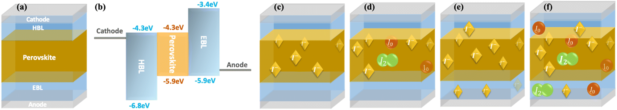 | ||
| Fig. 1 The simulated scenarios: (a) a solar cell without free iodides, as a reference (c) a solar cell in which the iodides cannot penetrate the blocking layers, (d) a solar cell in which the iodides cannot penetrate the blocking layers but can react, (e) a solar cell in which the iodides penetrate the blocking layers (f) a solar cell in which the iodides penetrate the blocking layers and can react, (b) the materials’ energy levels. | ||
We simulated four scenarios to investigate the effect of the ions and their various chemical reactions on the solar cells’ performance (see Fig. 1c–f). The first scenario (Fig. 1c) could be regarded as a reference for the perovskite PV devices where we introduce the ions but limit their activity to drift/diffuse within the perovskite active layer only.45 In the second case (Fig. 1d), we allow the iodine species to react and exchange electrons (or trap holes) with the perovskite semiconductor. We consider the devices in c and d to be a pair where the iodine species are confined to the perovskite layer. The second pair of devices are presented in Fig. 1e and f, where we enable the iodine species to penetrate the blocking layers.27,28 Again, we allow only transport for the first device (Fig. 1e), and in the second (Fig. 1f), we enable charge exchange with the layers and the contacts.
Boschloo and Hagfeldt presented a relatively detailed experimental study of iodide reactions and their relative energetics.34 Their work provides values and relations for the solution's reactions. Recently, Kerner et al.35 showed that these values might also serve as a rough guideline for the energetics to be expected in the solid state. Fig. 2a shows the values for the reactions’ energies extracted from ref. 34. On the same graph, we superimposed the energy levels of MAPbI3 taken from the reasonable range of experimental stoichiometries.46 It is interesting to note that in Fig. 2a, the lowest energy reaction (of p-doping the perovskite) has a 0.2 eV activation energy, while DFT calculations of this reaction in MAPbI3 predict 0.3 eV.17 Namely, the reactions’ energies fall roughly within the MAPbI3 band gap. The electrons could be exchanged with the lowest unoccupied molecular orbital (LUMO) or conduction band and the highest occupied molecular orbital (HOMO) or valence band levels. As our device simulation is limited to three species, we chose to work with I, I−, and I2 while ensuring a circular relation (Fig. 2b) that avoids irreversible paths, thus enabling also self-healing to occur.
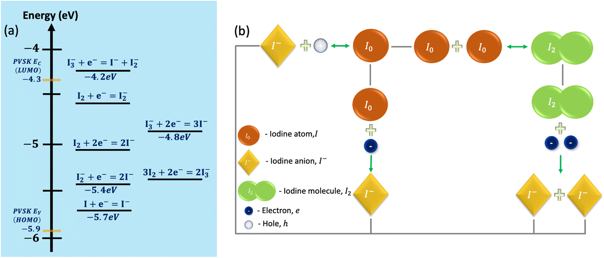 | ||
| Fig. 2 (a) Approximate positions of iodine/triiodide/diiodide/iodide reduction/oxidation potentials in acetonitrile relative to the valence and conduction bands of the MAPbI3 perovskite. (b) The reaction cycle considered in the simulation includes iodine atoms (I0), iodide anions (I−), iodine molecules (I2), and electrons and holes. The green arrows mark the reactions’ directions. | ||
The reactions we implemented are:
| I− + h → I (hole trapping or reduction at electrode) | (a) |
| I + eEv → I− (P doping = I → I− + h) | (b) |
| I + eEc → I− (electron trapping) | (c) |
| 2I ↔ I2 | (d) |
| I2 + 2eEC → 2I− (electron trapping) | (e) |
When the two species to react are at an intimate distance, the reaction rate would be strongly affected by energy activation (i.e.Fig. 2a) and overlap integrals between reactants and products. For low-mobility species, the reaction is often diffusion limited47 and Fig. 2a would only be used to determine the plausible reactions. For the (b) to (e) reaction rates, we used a diffusion-limited rate and employed the Smoluchowski rate coefficient for steady-state:47
| kD = 4πDABRAB | (1) |
We highlight that the chemical-physics picture was purposefully kept as simple as possible so that the effects of the iodine reactions would be directly observable. Specifically, this was achieved by choosing the BLs’ energy levels to perfectly align with the respective energy levels of the active perovskite layer. We implemented only radiative processes for recombination, and the SRH-type recombination48,49 is not included. This allows us to show that the electrochemical reactions introduce SRH-type recombination. A value within the range reported in the literature was selected for the ion (I−) and the atom (I) diffusion coefficients within the perovskite. Considering that it is to be expected that the molecule (I2) would diffuse slower, we chose its diffusion coefficient to be smaller by a factor of 10. For the ion diffusion within the blocking layer, we implemented four orders of magnitude lower diffusivities compared to the perovskite layer. Lastly, unless specifically indicated, we did not consider the irreversible loss of species as would be the case of ion intercalation into the electrode or I2 leakage. The parameters needed to reproduce our simulations on the Sentaurus device model are listed in Table S1 in the ESI† and the model's assumption are explicitly summarised there in Section I, ESI.†
If we do not implement any irreversible reactions, the device may eventually reach a steady state. Hence, the first results we present are for such a steady state. We ran a time-dependent simulation where at t = 0, ions and vacancies fully overlap in space within the perovskite layer. At t = 0, a 0.9 V bias is applied, the light turns on (at 1 sun intensity), and the ions start moving and reacting. After the devices reached a steady state, we ran a current density–voltage (J–V) scan at a 1 V s−1 rate.
Results
As shown in Fig. 2b, the hole-trapping reaction (a) is the precursor for the other electrochemical reactions, thus determining the overall effect. Hence it is best viewed as a fitting parameter within the current picture. Fig. 3 shows the JV characteristics of a high-efficiency solar cell with no trap-assisted recombination in red (see Table 1). To this cell, we introduce trap-assisted recombination through electrochemical reactions. Assuming relatively high mobility (for organics) of μe,h = 10−3 cm2 V−1 s−1 (Fig. 3a), adding an electron trapping coefficient rate of 10−11 cm3 s−1 (green line), the efficiency drops to 18%; for a rate of 5 × 10⁻¹¹ cm3 s−1 (blue line), it plummets to ∼9%. While demonstrating the critical role of reaction (trap) assisted recombination, it also helps us to ascertain that a value around 10−11 cm3 s−1 is appropriate for us to use for the rest of the paper.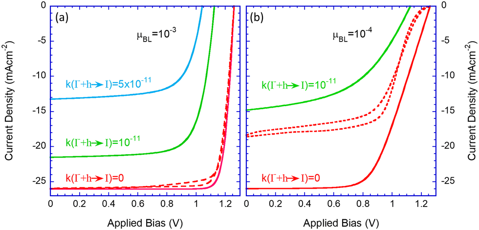 | ||
| Fig. 3 JV characteristics for hysteresis scan were obtained after the devices were held under one sun and 0.9 V to reach a steady state. The electron and hole mobility in the blocking layer was 10−3 cm2 V−1 s−1. (a) and 10−4 cm2 V−1 s−1 (b). The different line colours are for no ion reactions (red), a hole-trapping rate of 10−11 (green), and 5 × 10⁻¹¹ (blue). Full and dashed lines are for the blocking layers being blocking and permeable to ions, respectively. | ||
| k(I− + h → I) | 0 | 10−11 | 5 × 10⁻¹¹ |
| J SC mA cm−2 | 26 | 21.5 | 13.2 |
| V OC(V) | 1.27 | 1.12 | 1.05 |
| FF (%) | 88 | 75 | 68 |
| PCE (%) | 28 | 18 | 9.4 |
Fig. 3b examines the effect of low mobility or resistive blocking layers. It shows the known effects of serial resistance that reduces the fill factor (FF) and that the reduced extraction rate translates to reduced efficiency in the presence of reactions that introduce higher losses (green line). We will examine other effects of the resistive layers in the context of device degradation. Lastly, the results we discussed thus far were obtained assuming the blocking layers also block ions. As we will be discussing the effect of permeable blocking layers,27,28 we show in dashed red lines the results obtained for the ideal perovskite layer where the blocking layers are permeable to ions. The ion diffusion into the blocking layers changes the potential distribution within the device27,28 and in the case of resistive blocking layers it introduces efficiency loss and significant hysteresis (dashed red line in Fig. 3b).
Having demonstrated the role of the parameters’ values we move to investigate the internal distributions for a reasonably efficient device (i.e., μe,h_BL = 10−3 cm2 V−1 s−1; k(I− + h → I) ≤ 10−11). Fig. 4 depicts the density distribution of the electronic charges and iodine species in the devices at a steady state, under one Sun, and at 0.9 V. We remind the reader that I− represents all mobile iodide anions that could be within the crystal lattice (due to vacancies) or as interstitials (see Section I.B, ESI†). The sub-figures are arranged in a table format where the rows separate between ion-blocking BLs (top) and ion-permeable BLs (bottom). The columns distinguish between the scenarios in which the reactions are included (right) or not (left). Fig. 4a shows the known effect of ion motion within the perovskite layer (see inset to Fig. 4a). The depletion of mobile iodide at one end and its accumulation at the other contribute to screening any electric field and flattening the bands.45 These flat bands result in a flat distribution of electrons and holes. The symmetric nature of our chosen device structure makes the electron and hole densities almost equal, with slight differences due to the applied bias. In Fig. 4b, the device is as in Fig. 4a but with the reactions activated. The appearance of I0 indicates the presence of hole trapping (I− + h → I) and the I0 density can be viewed as the trap density for the subsequent electron capture (I + eEv → I−). This reaction (trap) assisted recombination36,38 is behind the slight downward shift of the electron/hole distribution in Fig. 4b relative to Fig. 4a. As discussed above, it also reflects in the lower PCE shown in Table 1.
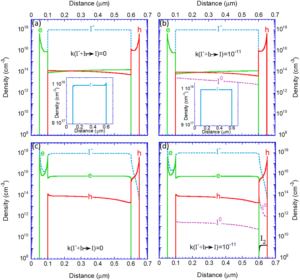 | ||
| Fig. 4 The electronic charges and the iodine species density distribution along the device after reaching steady state under illumination and at 0.9 V, which is close to the maximal power point of the solar cells. (a) A solar cell in which the iodides cannot penetrate the blocking layers (b) a solar cell in which the iodides cannot penetrate the blocking layers but can react within the perovskite layer (c) a solar cell in which the iodides penetrate the blocking layers (d) a solar cell in which the iodides penetrate the blocking layers and can react in the entire device. The insets to (a) and (b) show the iodide distribution on linear scale. | ||
In Fig. 4c, the reactions are off, and the ions can penetrate the blocking layers. The iodide (blue line) diffuses into the EBL and the HBL, leaving excess positive ionic charge within the perovskite layer. The drive towards charge neutrality implies that as iodides leave the perovskite, electrons accumulate within to compensate for the ionic space charge. The last statement implies that the iodide diffusion to the blocking layers turns the perovskite into an N-type semiconductor.
In Fig. 4d, the BLs are permeable to ions, and the iodide reactions are enabled within the entire device (but not with the electrodes). Compared to Fig. 4b, one observes a few differences. First, the imbalance between the electron and hole densities reduces the density of the iodine atom (I0). As the density of I0 dictates the electron trap rate, the reaction-assisted recombination is reduced. This manifests in a higher PCE (see Fig. S1 of the ESI†). Second, the lack of holes in the HBL implies no generation of I0, and the high electron density ensures that any I0 that diffuses in captures an electron to become I−. Thirdly, in the EBL the situation is reversed, and the high hole density ensures high I0 generation that essentially follows the iodide distribution. We note that the lack of electrons in the EBL also allows for a finite density of iodine molecules (I2) to evolve. It is interesting to note that the I2 generation is accelerated under 1 sun and that under dark conditions, it is at least 2 orders of magnitude smaller (see Fig. S2 in ESI†). This I2 generation will be discussed again in the context of device degradation.
To extend the picture further, we introduce non-reversible actions to the model. First, we examine the effect of the iodine molecule (I2) leaving the device as volatile species38,42 so that the reaction (e) does not occur. Second, we let the contacts react with the iodine species by absorbing it to mimic the effect of reactive contacts that immobilise the iodine/iodide by chemical reactions.
Regarding the I2 loss, as Fig. 4 shows, sizeable I2 generation takes place only at the electron blocking (hole transporting) layer (Fig. 4d). Since we observe iodide loss only for devices with ion-permeable blocking layers, we do not present the results for ion-blocking layers. Fig. 5a presents the simulated time evolution of the iodide density loss for a device biased at 0.9 V and under 1 sun illumination conditions. The lines’ colours follow the notation of Fig. 3 where red is for no reactions. Green is for k(I− + h → I) = 10−11, blue is for k(I− + h → I) = 5 × 10⁻¹¹, and black is for reactive contacts.
 | ||
| Fig. 5 Simulated time evolution of the iodide density loss for a device biased at 0.9 V and under 1 sun. (a) Conductive blocking layers (μBL = 10−3 cm2 V−1 s−1) (b) resistive blocking layers (μBL = 10−4 cm2 V−1 s−1). The loss is due to the assumption that I2 is lost through bubbling out. | ||
Fig. 5a shows that a combination of permeable blocking layers and reactive contacts is detrimental to device performance which is expected to degrade quickly on an hour scale. For the non-reactive contacts, the iodine molecules (I2) are allowed to leave the device as gas38,42,50 creating a longer-term loss of iodide. The time scale associated with this process is thousands of hours (top x-axis).
Fig. 5b shows similar results but for a device having resistive blocking layers (μBL = 10−4 cm2 V−1 s−1). Note that the degradation is about an order of magnitude faster compared to the conductive blocking layers depicted in Fig. 5a.
Discussion
We presented simulation results of perovskite solar cells that account for mobile ions. Furthermore, we considered, in the model, several iodine reactions. To distinguish the effect of the ions and the reactions on the perovskite solar cells, we compared four scenarios of solar cells; solar cells in which the iodine can’t penetrate the blocking layers, with and without reactions, solar cells in which the iodine can penetrate the blocking layers and reach the contacts, with and without reactions.As mentioned in the introduction, the question of what is moving in halide perovskites is not with a single answer,16–24 and in this paper, we circumvent this argument using a device model that does not distinguish between iodide motion within the crystal lattice (i.e. vacancies) or outside the crystal lattice (i.e. interstitials). Namely, we are dealing with mobile iodides.
For most of the paper, we limited ourselves to iodine reactions and ensured that our chosen set did not create an irreversible path. Specifically, we did not allow the I2 molecule to precipitate out, nor did we include structural degradation either in the electrode or inside the perovskite layer. Nevertheless, our model does show that the iodide transport into the blocking layers27 degrades the short-circuit current and that this effect is amplified in the case of resistive blocking layers (Fig. 3). We also found that the diffusion into the blocking layers results in the current degradation being accompanied by the appearance of a hysteresis.
The reactions themselves affect the device characteristics by introducing mobile recombination centres. The reactions cycle described in Fig. 2b shows that in the presence of mobile iodide, the reaction (I− + h → I) is the precursor for all other reactions and the appearance of iodine atoms (I0) and molecules (I2). Hence, we could treat the rate for this reaction as a fitting parameter while letting all other reactions be determined by their diffusion parameters (i.e. diffusion-limited reactions).47 Using Fig. 3a we determined the rate of 10−11 cm3 s−1 as appropriate representative of reasonably efficient devices.
Lastly, we examined the role of irreversible processes by introducing either I2 loss (I2 gas bubbling out) or implementing a contact that absorbs and immobilise the iodide. We found that I2 loss occurs only under light conditions, in agreement with ref. 38 and 42. The loss of iodide presented in Fig. 5 does not specify if it increases iodine vacancies (VI+) or reduces interstitial iodide (Ii−). The fact that the crystal has 1022–1023 cm−3 iodine atoms suggests that it would mainly manifest as enhanced vacancy formation. This implies that, at some stage, the perovskite crystal structure would start to fall apart. However, we are unaware of a method to link the loss of iodide with the degradation of the optoelectronic properties of the perovskite crystal. Hence, we only presented the time evolution of the iodide density loss (Fig. 5). Disregarding degradation mechanisms not captured by our model, these results suggest that a non-ion-blocking contact that also reacts and immobilises the iodide is detrimental to the device and would degrade it on the hour's scale (1–10 hours). For the device with ion-blocking contacts, if the iodine molecule is allowed to exit the device (i.e., leak out), the degradation is significantly slower but still in the 5 to 10 thousand hours range. Lastly, the effect of light and bias can be examined through Fig. S2 in the ESI.† Fig. S2a (ESI†) presents the same particle distributions shown in Fig. 4d. Fig. S2b (ESI†) shows that keeping the bias but moving to dark conditions results in two orders of magnitude lower generation of the I2 molecules. If we lower the bias to zero under dark conditions (Fig. S2c, ESI†), the I2 generation drops further by 16 orders of magnitude.
Conclusions
The above discussion leads us to our last conclusion that although our simulation model captures several experimentally reported phenomena, critical quantitative information regarding ion-related electrochemistry is missing. The timescales we reported above highly depend on the iodine species’ actual transport parameters, and we included only iodine chemistry. Also, our results suggest that for the perovskite cell to perform, the final “collision” step must limit some reactions. For example, the values we used as the rate for the I− + h → I are much slower than the transport (Langevin) recombination. A slow final recombination step (“collision”) would typically be associated with a significant activation energy required for the given recombination-reaction. High activation energies could be due to differences in the atoms’ position (configuration coordinates) before and after the recombination (i.e., between reactants and products). The more stable perovskite compositions could very well be those with larger activation (reorganisation) energies that suppress the I− + h → I reaction. Designing a composition with these energies in mind should open new opportunities for long-term stability cells.Lastly, the reactions’ energy diagram (Fig. 2a) suggests that for perovskite structures having deep valence bands, the I− + h → I reaction of hole trapping is inevitable. In such a case, avoiding the formation and loss of I2 would be difficult. Namely, irreversible degradation is only a matter of time and will likely be too short for standard PV applications. However, without I2 loss, the cell can self-heal during non-illumination times (such as nighttime). Another approach would be to interfere with the I2 generation or the bimolecular reaction I0 + I0 → I2. As this was found to be significant only within the EBL, one must choose (design) the EBL accordingly. Within this model's framework, this can only be done by eliminating the I− + h → I0 reaction. In other words, designing the blocking layer such that this reaction is blocked or that the iodine would be an efficient electron acceptor (p-dopant, I + eEv → I−).
Author contributions
S. B. conducted the simulation work. S. B. and N. T. wrote the paper.Conflicts of interest
There are no conflicts to declare.Acknowledgements
This research was supported by the Ministry of Innovation, Science and Technology Israel, the M-ERANET grant PHANTASTIC Call 2021, the Adelis Foundation for renewable energy research within the framework of the Grand Technion Energy Program (GTEP), and the Technion Ollendorff Minerva Center. S. B. is a fellow of the Ariane de Rothschild Women’s Doctoral Programme.References
- M. Kato, T. Fujiseki, T. Miyadera, T. Sugita, S. Fujimoto, M. Tamakoshi, M. Chikamatsu and H. Fujiwara, J. Appl. Phys., 2017, 121, 115501 CrossRef.
- K. P. Goetz, A. D. Taylor, F. Paulus and Y. Vaynzof, Adv. Funct. Mater., 2020, 1910004 CrossRef CAS.
- D. R. Ceratti, Y. Rakita, L. Cremonesi, R. Tenne, V. Kalchenko, M. Elbaum, D. Oron, M. A. C. Potenza, G. Hodes and D. Cahen, Adv. Mater., 2018, 30, 1706273 CrossRef PubMed.
- K. X. Steirer, P. Schulz, G. Teeter, V. Stevanovic, M. Yang, K. Zhu and J. J. Berry, ACS Energy Lett., 2016, 1, 360–366 CrossRef CAS.
- M. M. Lee, J. Teuscher, T. Miyasaka, T. N. Murakami and H. J. Snaith, Science, 2012, 338, 643–647 CrossRef CAS PubMed.
- L. Schmidt-Mende, V. Dyakonov, S. Olthof, F. Ünlü, K. M. T. Lê, S. Mathur, A. D. Karabanov, D. C. Lupascu, L. M. Herz, A. Hinderhofer, F. Schreiber, A. Chernikov, D. A. Egger, O. Shargaieva, C. Cocchi, E. Unger, M. Saliba, M. M. Byranvand, M. Kroll, F. Nehm, K. Leo, A. Redinger, J. Höcker, T. Kirchartz, J. Warby, E. Gutierrez-Partida, D. Neher, M. Stolterfoht, U. Würfel, M. Unmüssig, J. Herterich, C. Baretzky, J. Mohanraj, M. Thelakkat, C. Maheu, W. Jaegermann, T. Mayer, J. Rieger, T. Fauster, D. Niesner, F. Yang, S. Albrecht, T. Riedl, A. Fakharuddin, M. Vasilopoulou, Y. Vaynzof, D. Moia, J. Maier, M. Franckevičius, V. Gulbinas, R. A. Kerner, L. Zhao, B. P. Rand, N. Glück, T. Bein, F. Matteocci, L. A. Castriotta, A. Di Carlo, M. Scheffler and C. Draxl, APL Mater., 2021, 9, 109202 CrossRef CAS.
- NREL, 2021.
- Q. Sun, P. Fassl, D. Becker-Koch, A. Bausch, B. Rivkin, S. Bai, P. E. Hopkinson, H. J. Snaith and Y. Vaynzof, Adv. Energy Mater., 2017, 1700977, DOI:10.1002/aenm.201700977.
- Y. Ouyang, L. Shi, Q. Li and J. Wang, Small Methods, 2019, 3, 1900154 CrossRef.
- F. Galatopoulos, I. T. Papadas, G. S. Armatas and S. A. Choulis, Adv. Mater. Interfaces, 2018, 5, 1800280 CrossRef.
- G. Abdelmageed, L. Jewell, K. Hellier, L. Seymour, B. Luo, F. Bridges, J. Z. Zhang and S. Carter, Appl. Phys. Lett., 2016, 109, 233905 CrossRef.
- N. K. Kim, Y. H. Min, S. Noh, E. Cho, G. Jeong, M. Joo, S. W. Ahn, J. S. Lee, S. Kim, K. Ihm, H. Ahn, Y. Kang, H. S. Lee and D. Kim, Sci. Rep., 2017, 7, 4645 CrossRef PubMed.
- X. Zhang, X. Chen, Y. Chen, N. A. Nadege Ouedraogo, J. Li, X. Bao, C. B. Han, Y. Shirai, Y. Zhang and H. Yan, Nanoscale Adv., 2021, 3, 6128–6137 RSC.
- Y. Zhao, W. Zhou, Z. Han, D. Yu and Q. Zhao, Phys. Chem. Chem. Phys., 2021, 23, 94–106 RSC.
- D. Zhang, D. Li, Y. Hu, A. Mei and H. Han, Commun. Mater., 2022, 3, 58 CrossRef.
- J. M. Frost and A. Walsh, Acc. Chem. Res., 2016, 49, 528–535 CrossRef CAS PubMed.
- S. G. Motti, D. Meggiolaro, S. Martani, R. Sorrentino, A. J. Barker, F. De Angelis and A. Petrozza, Adv. Mater., 2019, 31, 1901183 CrossRef CAS PubMed.
- S. T. Birkhold, J. T. Precht, H. Liu, R. Giridharagopal, G. E. Eperon, L. Schmidt-Mende, X. Li and D. S. Ginger, ACS Energy Lett., 2018, 3, 1279–1286 CrossRef CAS.
- D. R. Ceratti, A. V. Cohen, R. Tenne, Y. Rakita, L. Snarski, N. P. Jasti, L. Cremonesi, R. Cohen, M. Weitman, I. Rosenhek-Goldian, I. Kaplan-Ashiri, T. Bendikov, V. Kalchenko, M. Elbaum, M. A. C. Potenza, L. Kronik, G. Hodes and D. Cahen, Mater. Horiz., 2021, 8, 1570–1586 RSC.
- C. C. Boyd, R. Cheacharoen, T. Leijtens and M. D. McGehee, Chem. Rev., 2019, 119, 3418–3451 CrossRef CAS PubMed.
- C. Li, A. Guerrero, Y. Zhong, A. Gräser, C. A. M. Luna, J. Köhler, J. Bisquert, R. Hildner and S. Huettner, Small, 2017, 13, 1701711 CrossRef PubMed.
- J. M. Azpiroz, E. Mosconi, J. Bisquert and F. De Angelis, Energy Environ. Sci., 2015, 8, 2118–2127 RSC.
- S. Reichert, J. Flemming, Q. An, Y. Vaynzof, J.-F. Pietschmann and C. Deibel, Phys. Rev. Appl., 2020, 13, 034018 CrossRef CAS.
- P. Fassl, S. Ternes, V. Lami, Y. Zakharko, D. Heimfarth, P. E. Hopkinson, F. Paulus, A. D. Taylor, J. Zaumseil and Y. Vaynzof, ACS Appl. Mater. Interfaces, 2019, 11, 2490–2499 CrossRef CAS PubMed.
- M. Pazoki, T. J. Jacobsson, S. H. T. Cruz, M. B. Johansson, R. Imani, J. Kullgren, A. Hagfeldt, E. M. J. Johansson, T. Edvinsson and G. Boschloo, J. Phys. Chem. C, 2017, 121, 26180–26187 CrossRef CAS.
- C. Besleaga, L. E. Abramiuc, V. Stancu, A. G. Tomulescu, M. Sima, L. Trinca, N. Plugaru, L. Pintilie, G. A. Nemnes, M. Iliescu, H. G. Svavarsson, A. Manolescu and I. Pintilie, J. Phys. Chem. Lett., 2016, 7, 5168–5175 CrossRef CAS PubMed.
- S. Bitton and N. Tessler, J. Mater. Chem. C, 2021, 9, 1888–1894 RSC.
- S. Bitton and N. Tessler, Appl. Phys. Lett., 2020, 117, 133904 CrossRef CAS.
- C. Eames, J. M. Frost, P. R. F. Barnes, B. C. O’Regan, A. Walsh and M. S. Islam, Nat. Commun., 2015, 6, 7497 CrossRef CAS PubMed.
- B. Rivkin, P. Fassl, Q. Sun, A. D. Taylor, Z. Chen and Y. Vaynzof, ACS Omega, 2018, 3, 10042–10047 CrossRef CAS PubMed.
- M. H. Futscher, J. M. Lee, L. McGovern, L. A. Muscarella, T. Wang, M. I. Haider, A. Fakharuddin, L. Schmidt-Mende and B. Ehrler, Mater. Horiz., 2019, 6, 1497–1503 RSC.
- S. Tammireddy, S. Reichert, Q. An, A. D. Taylor, R. Ji, F. Paulus, Y. Vaynzof and C. Deibel, ACS Energy Lett., 2022, 7, 310–319 CrossRef CAS.
- S. Reichert, Q. An, Y.-W. Woo, A. Walsh, Y. Vaynzof and C. Deibel, Nat. Commun., 2020, 11, 6098 CrossRef CAS PubMed.
- G. Boschloo and A. Hagfeldt, Acc. Chem. Res., 2009, 42, 1819–1826 CrossRef CAS PubMed.
- R. A. Kerner, S. Heo, K. Roh, K. Macmillan, B. W. Larson and B. P. Rand, ACS Energy Lett., 2021, 6, 501–508 CrossRef CAS.
- L. Bertoluzzi, J. B. Patel, K. A. Bush, C. C. Boyd, R. A. Kerner, B. C. O'Regan and M. D. McGehee, Adv. Energy Mater., 2021, 11, 2002614 CrossRef CAS.
- D. Meggiolaro, S. G. Motti, E. Mosconi, A. J. Barker, J. Ball, C. Andrea Riccardo Perini, F. Deschler, A. Petrozza and F. De Angelis, Energy Environ. Sci., 2018, 11, 702–713 RSC.
- S. G. Motti, D. Meggiolaro, A. J. Barker, E. Mosconi, C. A. R. Perini, J. M. Ball, M. Gandini, M. Kim, F. De Angelis and A. Petrozza, Nat. Photonics, 2019, 13, 532–539 CrossRef CAS.
- R. A. Kerner, Z. Xu, B. W. Larson and B. P. Rand, Joule, 2021, 5, 2273–2295 CrossRef CAS.
- Z. Xu, R. A. Kerner, J. J. Berry and B. P. Rand, Adv. Funct. Mater., 2022, 32, 2203432 CrossRef CAS.
- J. A. Kress, C. Quarti, Q. An, S. Bitton, N. Tessler, D. Beljonne and Y. Vaynzof, ACS Energy Lett., 2022, 7, 3302–3310 CrossRef CAS PubMed.
- F. Fu, S. Pisoni, Q. Jeangros, J. Sastre-Pellicer, M. Kawecki, A. Paracchino, T. Moser, J. Werner, C. Andres, L. Duchêne, P. Fiala, M. Rawlence, S. Nicolay, C. Ballif, A. N. Tiwari and S. Buecheler, Energy Environ. Sci., 2019, 12, 3074–3088 RSC.
- C. Li, S. Tscheuschner, F. Paulus, P. E. Hopkinson, J. Kießling, A. Köhler, Y. Vaynzof and S. Huettner, Adv. Mater., 2016, 28, 2446–2454 CrossRef CAS PubMed.
- Y. Kato, L. K. Ono, M. V. Lee, S. Wang, S. R. Raga and Y. Qi, Adv. Mater. Interfaces, 2015, 2, 1500195 CrossRef.
- N. Tessler and Y. Vaynzof, ACS Energy Lett., 2020, 5, 1260–1270 CrossRef CAS.
- P. Fassl, V. Lami, A. Bausch, Z. Wang, M. T. Klug, H. J. Snaith and Y. Vaynzof, Energy Environ. Sci., 2018, 11, 3380–3391 RSC.
- S. A. Rice, in Diffusion-Limited Reactions, ed. C. H. Bamford, C. F. H. Tipper and R. G. Compton, Elsevier, 1985, vol. 25, pp. 3–46 Search PubMed.
- Q. An, F. Paulus, D. Becker-Koch, C. Cho, Q. Sun, A. Weu, S. Bitton, N. Tessler and Y. Vaynzof, Matter, 2021, 4, 1683–1701 CrossRef CAS.
- S. Bitton, Q. An, Y. Vaynzof and N. Tessler, ACS Appl. Energy Mater., 2021, 4, 8709–8714 CrossRef CAS.
- G. Y. Kim, A. Senocrate, T.-Y. Yang, G. Gregori, M. Grätzel and J. Maier, Nat. Mater., 2018, 17, 445–449 CrossRef CAS PubMed.
Footnote |
| † Electronic supplementary information (ESI) available: Simulations’ parameters and additional results. See DOI: https://doi.org/10.1039/d3ee00881a |
| This journal is © The Royal Society of Chemistry 2023 |