
 Open Access Article
 This Open Access Article is licensed under a Creative Commons Attribution-Non Commercial 3.0 Unported Licence
Antimonene: a tuneable post-graphene material for advanced applications in optoelectronics, catalysis, energy and biomedicine
Jose A.
Carrasco†
 ,
Pau
Congost-Escoin†
,
Mhamed
Assebban
and
Gonzalo
Abellán
*
,
Pau
Congost-Escoin†
,
Mhamed
Assebban
and
Gonzalo
Abellán
*
Instituto de Ciencia Molecular (ICMol), Universidad de Valencia, Catedrático José Beltrán Martínez, 2, 46980 Paterna, Spain. E-mail: gonzalo.abellan@uv.es
First published on 6th February 2023
Abstract
The post-graphene era is undoubtedly marked by two-dimensional (2D) materials such as quasi-van der Waals antimonene. This emerging material has a fascinating structure, exhibits a pronounced chemical reactivity (in contrast to graphene), possesses outstanding electronic properties and has been postulated for a plethora of applications. However, chemistry and physics of antimonene remain in their infancy, but fortunately recent discoveries have shed light on its unmatched allotropy and rich chemical reactivity offering a myriad of unprecedented possibilities in terms of fundamental studies and applications. Indeed, antimonene can be considered as one of the most appealing post-graphene 2D materials reported to date, since its structure, properties and applications can be chemically engineered from the ground up (both using top-down and bottom-up approaches), offering an unprecedented level of control in the realm of 2D materials. In this review, we provide an in-depth analysis of the recent advances in the synthesis, characterization and applications of antimonene. First, we start with a general introduction to antimonene, and then we focus on its general chemistry, physical properties, characterization and synthetic strategies. We then perform a comprehensive study on the allotropy, the phase transition mechanisms, the oxidation behaviour and chemical functionalization. From a technological point of view, we further discuss the applications recently reported for antimonene in the fields of optoelectronics, catalysis, energy storage, cancer therapy and sensing. Finally, important aspects such as new scalable methodologies or the promising perspectives in biomedicine are discussed, pinpointing antimonene as a cutting-edge material of broad interest for researchers working in chemistry, physics, materials science and biomedicine.
 Jose A. Carrasco | Jose Alberto Carrasco obtained his degree in Chemistry from the University of Valencia (UV) in 2012. Afterwards, he received his Master's degree in Nanoscience and Nanotechnology in 2014. From 2014 to 2018 he pursued his PhD supervised by Prof. Eugenio Coronado and Dr. Gonzalo Abellán at the Institute of Molecular Science (ICMol, UV), focusing on inorganic two-dimensional materials. Thereafter, he worked as a postdoctoral fellow in the 2D-Chem group at ICMol (2019–2020) working on 2D-pnictogens, and at the Institute of Chemical Technology (ITQ) under the supervision of Dr. Antonio Leyva-Pérez, working in catalysis (CSIC-UPV, 2021). Now he is working in his true passion as a teacher of physics and chemistry, sharing his love for science to the younger generations. |
 Pau Congost-Escoin | Pau Congost-Escoin received his BSc in Biochemistry and Biomedical sciences from the University of Valencia (UV) in 2020, and a Master's degree in Nanoscience and Nanotechnology in 2021, when he started working on 2D materials. He is currently a PhD student in Nanoscience and Nanotechnology at ICMol (UV), under the supervision of Dr. Gonzalo Abellán, working on the biomedical applications of 2D pnictogens. His research interest lies in the interactions of 2D materials in biological environments and the mechanisms governing them. |
 Mhamed Assebban | Mhamed Assebban obtained his BSc in Chemical engineering and materials science at the University of Abdelmalek Essaadi in 2009 and his Master’s degree in 2011. He obtained his PhD in 2016 at the same university, in a collaborative research project with the University of Bielefeld in Germany, where he developed efficient heterogeneous catalysts for the removal of toxic atmospheric gases. He joined the Zentralinstitut für neue Materialien und Prozesstechnik (ZMP, FAU) in Germany as a postdoctoral researcher in 2018, and then he moved to the Institute of Molecular Science (ICMol) at the University of Valencia in Spain under the supervision of Dr. Gonzalo Abellán. In 2020 he returned back to occupy the same position at the ZMP in Fürth where he focuses his research work on the study of novel 2D materials by tuning their physical and chemical properties to make them even more suitable for different applications, such as energy storage, catalysis and optoelectronics. |
 Gonzalo Abellán | Gonzalo Abellán obtained his PhD in nanoscience and nanotechnology in 2014 from the University of Valencia. Afterwards he gained a self-driven Marie Curie Fellowship and joined Prof. Andreas Hirsch's group at the Friedrich-Alexander-Universität, Erlangen-Nürnberg. In 2018 he returned to Spain as an Excellence Distinguished Researcher after getting a GenT-CIDEGENT contract (Generalitat Valenciana), the Ramón y Cajal fellowship, and the ERC Starting Grant, among others. Gonzalo Abellán's main research activities have been focused on three lines: 2D-pnictogens (group of P, As, Sb and Bi), layered hydroxides, and carbon nanoforms and related hybrid materials, with a special emphasis on energy-related applications. He is the leader of the 2D-Chem research group at the Institute of Molecular Science (ICMol, UV). |
1. Introduction
Since the isolation of phosphorene, the two-dimensional (2D)-pnictogen (P, As, Sb and Bi) science has emerged as one of the main topics in 2D materials.1–11 Indeed, 2D materials from group 15 of the periodic table offer a great variety of structures, properties and reactivities as a consequence of the progressive increase in the intensity of the interlayer bonds as one goes down the group, passing from purely van der Waals (vdW) materials such as phosphorene to materials with a marked covalent character that makes them quasi-vdW, as is the case with heavy pnictogens (Sb & Bi).12–15 The importance of these interactions in the physical and chemical properties of 2D-pnictogens is crucial and differentiates them from the rest of Xenes. This makes heavy 2D-pnictogens, and antimonene in particular, one of the most attractive materials in the field, as it opens the door to chemically engineer their properties from scratch.This review provides a comprehensive analysis and updated study of antimonene, a material that since its prediction in 2015 and later isolation in 2016 has attracted increasing attention due to its unique electronic properties (thermoelectric, semiconducting, topological insulator, nonlinear optic, etc.) and its unmatched atomic structure and chemical flexibility, which allow its exotic (inter-allotropic) phase engineering. Moreover, this review thoroughly analyses (>200 articles) the state-of-the-art of antimonene research, highlighting the recent progress in its experimental preparation with a strong emphasis on its properties, chemical reactivity, functionalization, and the potential applications reported to date. Despite the fact that there are a few reviews focused on pnictogens as a family of emerging materials, this work intends to address the antimonene state-of-the-art from in-depth and critical chemical points of view. To the best of our knowledge this approach has not been addressed to date. Indeed, in a post-graphene era, antimonene holds great promise for the development of fundamental science such as novel van der Waals (and beyond) heterostructures, molecular interface engineering, DNA sensors, high-performance (opto)electronic devices, modern Na-ion batteries and many other scientific challenges to come. Scheme 1 summarizes the different synthetic approaches and main applications of this fascinating material, which will be detailed below, including a brief historical note about the origin of antimony and its properties.
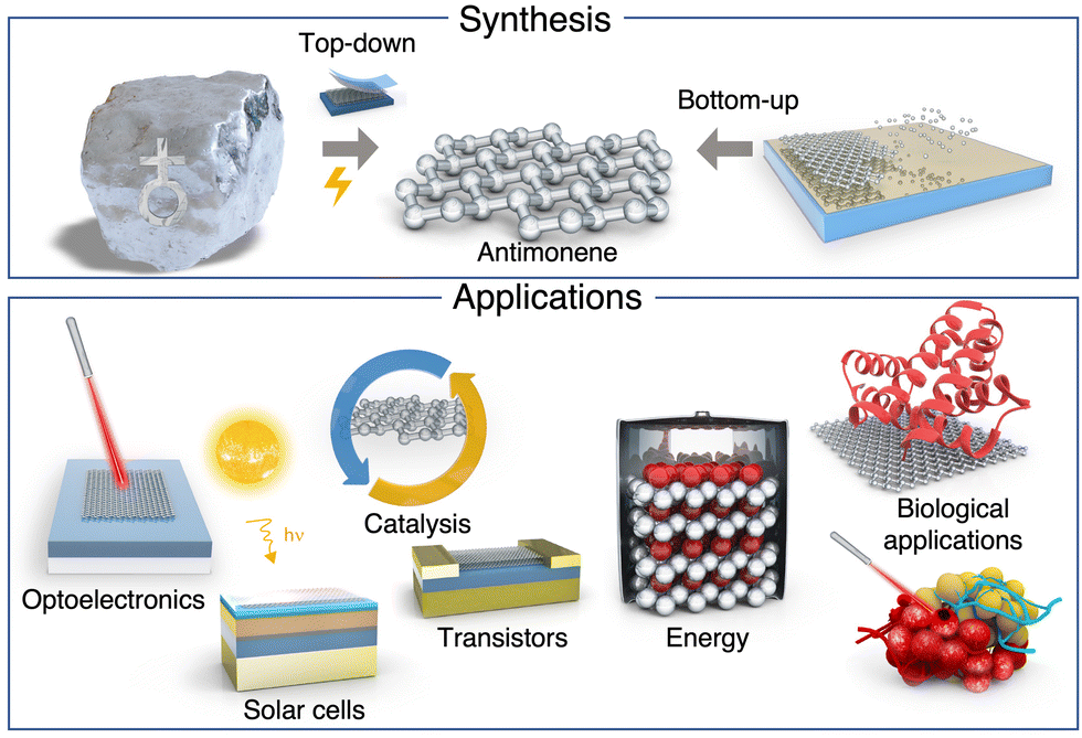 | ||
| Scheme 1 Summary of antimonene synthesis and applications. The image above represents (top) the synthesis of antimonene from bulk antimony or via the assembly of antimony atoms on a substrate and (bottom) the applications of antimonene as a multifunctional material. From left to right: optoelectronic devices, solar cells, catalysis, field-effect transistors, energy storage, biomedical applications by binding molecules of interest and destroying carcinogenic cells. | ||
1.1 History of antimony and general properties
Antimony (symbol Sb, from the Latin stibium and derived from the Greek word referring to the use of stibnite) has been known since ancient times (ca. 4000 BC) and has been used in the form of cosmetics, medications, colouring agent for glass and casting pottery, to name a few. In this sense, ancient Egyptians used antimony in the form of stibnite (Sb2S3) as a rouge for lips. Similarly, ancient Romans used stibnite in a medical way or as black eye make-up.16 The name antimony comes from two different Greek words: anti, which means not and monos, whose meaning refers to alone. This compound noun is due to the rare appearance of isolated antimony in nature while is commonly found as combined with both metals and non-metals.The use of Sb was also described by medieval alchemists in the 15th century. The element intrigued the alchemists due to its similar properties to those of gold and the fact that it cannot be dissolved with aqua regia, hence being a good candidate for its transmutation into gold.17 During the 16th century, Paracelsus and his followers promoted the use of antimony and other metals as drugs. This statement was in stark contrast with the teachings of Galen (ca. 2nd century) who considered the use of metals as poisonous.18 In this context, the period between ca. 1560 and 1660 was coined as the antimony war due to the strong conflict between the Galenic medicine against the medical practices of Paracelsus.
Even though the original discoverer of Sb remains unknown, Nicolas Lémery, a French chemist, was the first one to scientifically study both antimony and its compounds, publishing his findings in 1707. Antimony compounds have been used for centuries in the treatment of schistosomiasis and leishmaniasis;19 however, one of the most recognisable aspects of antimony is its toxicity,20 since it can even cause death by intoxication and its symptoms are disguised as general gastric disorders. The poisonous activity comes from its ability to be attached to particular enzymes because of its high affinity to the sulphur atoms of the enzyme's active site. Regarding the different species, one of the deadliest compounds of antimony is the gas stibine (SbH3). Most antimony compounds such as stibine or oxides (Sb2O3, Sb2O5, etc.) can be absorbed from the respiratory tract due to the low particle size, therefore being retained in the organism for longer periods than larger particles.21
From the economic point of view and regarding the applications of antimony and its compounds, the element is a metalloid with an important impact. The actual annual production is at around 185![[thin space (1/6-em)]](https://www.rsc.org/images/entities/char_2009.gif) 000 tonnes per year, with 85% coming from China. Additional producers can be found in countries like Russia, South Africa or Bolivia, among others. The main ores are in the form of stibnite and tetrahedrite, this one being a copper antimony sulfosalt mineral with formula: (Cu,Fe)12Sb4S13, which yields Sb as a by-product.17 Stibnite is easily separated from other minerals due to its low melting point of 546 °C. Afterwards, the roasting of stibnite produces Sb2O3 or Sb2O4 which can be both reduced to elemental Sb with coke. An alternative method to obtain Sb is to directly reduce the stibnite with scrap iron, followed by a purification procedure with sodium nitrate and sodium carbonate.22,23Fig. 1 schematizes the production of elemental Sb from stibnite.
000 tonnes per year, with 85% coming from China. Additional producers can be found in countries like Russia, South Africa or Bolivia, among others. The main ores are in the form of stibnite and tetrahedrite, this one being a copper antimony sulfosalt mineral with formula: (Cu,Fe)12Sb4S13, which yields Sb as a by-product.17 Stibnite is easily separated from other minerals due to its low melting point of 546 °C. Afterwards, the roasting of stibnite produces Sb2O3 or Sb2O4 which can be both reduced to elemental Sb with coke. An alternative method to obtain Sb is to directly reduce the stibnite with scrap iron, followed by a purification procedure with sodium nitrate and sodium carbonate.22,23Fig. 1 schematizes the production of elemental Sb from stibnite.
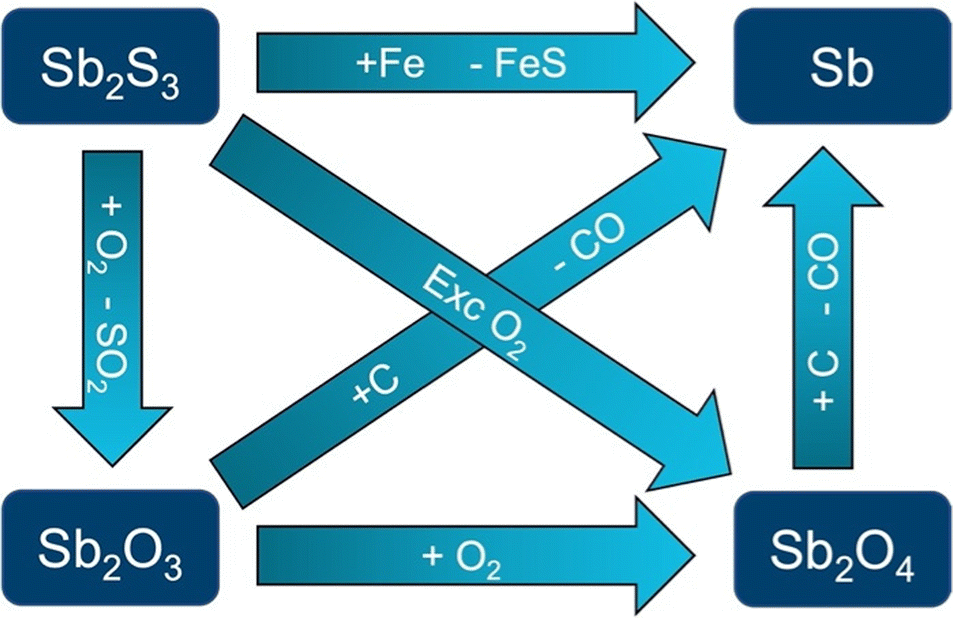 | ||
| Fig. 1 Schematic representation of the production of elemental antimony from stibnite. Adapted from ref. 23 with permission from John Wiley & Sons, copyright 2011. | ||
With respect to the main applications, antimony compounds can be used in different fields such as flame retardants (Sb2O3), catalysis (SbF5), pyrotechnical articles (Sb2S3 + H2S) or in electronics (alloyed with Ga and As).17,24 Related to electronic applications, Sb is mainly used in semiconductor devices such as diodes and infrared detectors. Alloying with Pb or other metals can enhance its hardness and strength. In this sense, a wide variety of alloys are described with Na, K, Ag, Au, Mg, Zn or Al, to name a few,25 leading to additional applications like cable and bullet sheathing as well as its use in batteries in the form of a Sb–Pb alloy.26
From the chemical point of view, Sb is considered a metalloid element, a member of the group 15 in the periodic table, i.e., the family of pnictogens and with an electronic configuration of [Kr] 4d10 5s2 5p3. Regarding the position of pnictogens in the periodic table, it is not unusual to come across some papers that refer to group VA instead of group 15. Here, we want to point out the fact that this old nomenclature based on roman numbers and capital letters A/B has been discarded by the IUPAC since 1990.27 Therefore, the only correct labelling nowadays for the pnictogen group is 15. Sb can appear in two different forms: while the metallic one is bright, slivery, hard and brittle (and resembles Pb), the non-metallic one is a grey powder. Furthermore, it poorly conducts both electricity and temperature, whereas it shows good stability in dry air and is not affected by dilute acids or alkalis. Additionally, upon cooling, Sb and some of its alloys expand.28 The most common oxidation states are (+3) and (+5) as found in nature. Some typical compounds for the trivalent and pentavalent antimony are SbCl3 and Sb2O5, respectively. However, additional oxidation states of (−3) (stibine, SbH3) and (0) (Sb metal) are also described,29 as well as mixed oxidation state compounds.30 The inorganic chemistry of Sb is extremely rich and mostly focused on both (+3) and (+5) oxidation states. In this context, there are several studies reporting antimony hydrides (SbH3), compounds with elements of group 13 or 14 (GaSb, Sb(SiMe3)), with other pnictogens such as N or P (Sb(NR2)), antimony chalcogens (Sb2O3, Sb2(SO4)3, Sb2S3), antimony halides (SbCl3, SbF5) or antimonides with Sb3− such as Li3Sb or Na3Sb, to name a few.23 Although it appears mainly in inorganic compounds, Sb also has a rich organometallic chemistry.31 After the synthesis of the first trialkyl antimony compounds in around 1850 – trimethyl- and triethylstibine – an incredible variety of organoantimony compounds have been reported to date, mainly in the oxidation states of (+3) and (+5). Trivalent Sb can be found in tertiary stibines, organoantimony(III) halides and pseudohalides, diorganoantimony cations and anions, or organoantimony hydrides, to name a few. On the other hand, regarding the pentavalent organoantimony compounds, one can find triorganoantimony(V) compounds, penta alkyls and aryls or organoantimony(V) chalcogen and nitrogen derivatives. Additionally, there are other organometallic compounds such as transition metal complexes with organoantimony ligands, low-coordination organoantimony derivatives and organometallic compounds with covalent single Sb–Sb bonds, including distibines, cyclostibines catena-stibines or polycicles.32
The abundance of the element corresponds to ca. 0.00002% of the Earth's crust, and with respect to the existence of isotopes, there are 37 known Sb isotopes, with masses that vary from 103 to 139 u. In this context, there are two naturally stable isotopes: Sb-121 (57%) and Sb-123 (43%). Some isotopes are radioactive and produced after fission experiments. Among these, Sb-125 is the longest-lived radioisotope, with a half-life of 2.76 years.33 Additional elemental parameters of Sb can be found in Table 1.
| Parameter | Value | Parameter | Value |
|---|---|---|---|
| Year of discovery | Known from ca. 4000 B.C., studied by Nicolas Lémery (1707) | Magnetic type | Diamagnetic |
| Alchemy symbol |
|
Molar magnetic susceptibility (m3 mol−1) | −1.327 × 10⁻⁹ |
| Atomic number | 51 | Electronic shell | [Kr] 4d10 5s2 5p3 |
| Atomic mass (g mol−1) | 121.75 | Standard potential (V) | 0.21 (Sb3+/Sb) |
| 0.60 (Sb2O5/SbO+) | |||
| −0.51 (Sb/SbH3) | |||
| Density (g cm−3) | 6.684 | Natural isotopes, abundance and radioactive stability | 121Sb (57.4%, stable) |
| 123Sb (42.6%, stable) | |||
| Melting point (°C) | 631 | Abundance in Earth's crust | 0.00002% |
| Boiling point (°C) | 1587 | Nuclear spin, I | 121Sb (+5/2) |
| 123Sb (+7/2) | |||
| Heat of fusion (kJ mol−1) | 19.7 | Ionization energies (kJ mol−1) | |
| Heat of vaporization (kJ mol−1) | 67 | M → M+ | 833.7 |
| Specific heat (J kg−1 K−1) | 207 | M+ → M2+ | 1794 |
| Thermal conductivity (W m−1 K−1) | 24 | M2+ → M3+ | 2443 |
| Bulk modulus (GPa) | 42 GPa | M3+ → M4+ | 4260 |
| Shear modulus (GPa) | 20 | M4+ → M5+ | 5400 |
| Young modulus (GPa) | 55 | Electron affinity (kJ mol−1) | 101 |
| M → M− | |||
| Mohs hardness | 3 | Electronegativity, χP (Pauling scale) | 2.05 |
| Space group name |
R![[3 with combining macron]](https://www.rsc.org/images/entities/char_0033_0304.gif) m m |
Atomic radius (Å) | 1.82 |
| Electrical type | Conductor | Single-bond covalent radius (Å) | 1.41 |
| Electrical conductivity (S m−1) | 2.5 × 10⁶ | van der Waals radius (Å) | 2.20 |
| Resistivity (m Ω) | 4 × 10⁻⁷ | Ionic radii (Å) | M3+ 0.62 |
| M5+ 0.76 |
Concerning the existence of allotropes, elemental bulk Sb has three known allotropes: explosive, black and gray.22 The most common form is the gray allotrope, with a rhombohedral structure like gray arsenic and a typical semi metallic behaviour. Black antimony is analogous to red phosphorus and explosive antimony usually evolve to the gray one after mechanical stress or on heating.34 While other pnictogens such as P and As depict α and β layered stable phases, the heavy pnictogens Sb and Bi have their most stable phase as the β allotrope even though other allotropes are theoretically predicted and recently obtained under certain conditions, which will be detailed below.35,36Fig. 2 summarizes the different layered crystal structures and stable phases.34
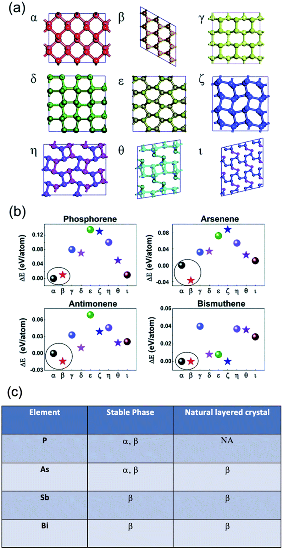 | ||
| Fig. 2 (a) Typical honeycomb and non-honeycomb structures of 2D pnictogen allotropes. (b) Average binding energies of the different allotropes, highlighting the β phase as the most stable in average. (c) Table summarizing the stable phases of the different pnictogens. While α phase presents a parallel puckered layer with space group of Cmca, β phase exhibits parallel buckled layers with the Rm space group in a rhombohedral structure. Adapted from ref. 34 with permission from Royal Society of Chemistry, copyright 2018. | ||
1.2 2D materials: cutting-edge for the 21st century
After the rise of graphene in 2004,37–39 a myriad of new graphene-like two-dimensional (2D) materials have arisen.40–43 The number of documents by year related to the topic of 2D materials keeps growing and has reached a maximum of ca. 17000 papers by mid-2022 (source: Scopus). Fig. 3 depicts the total number of papers related specifically to 2D-pnicotegns. This trend is motivated for the outstanding properties of these materials towards new applications in the fields of energy, electronics, catalysis, topological insulators, thermal management or anisotropic magnetization.40
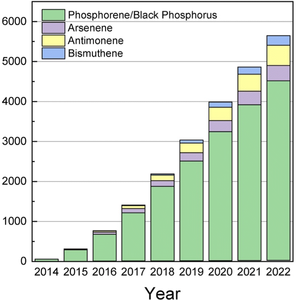 | ||
| Fig. 3 Graphic showing the cumulative number of papers focused on 2D pnictogens. Data acquired from Scopus on October 2022. | ||
The wide variety of 2D materials that are described in the literature can be divided into three main groups: the layered van der Waals (vdW) solids, the 3D covalent/ionic solids, and the layered ionic solids. This classification is based on the main forces that ensemble the layered structure, i.e., intermolecular van der Waals interactions or electrostatic forces. While in the first group one can find materials such as graphene, boron nitride or layered metal dichalcogenides,40,44 the second group is composed of covalent materials that can be exfoliated down to the 2D limit (i.e. germanene) or 3D ionic solids (like iron oxide) that can be exfoliated by controlling parameters such as the energy of cleavage planes or the stabilization energy of the nanolayers. Finally, the third group includes charged 2D layers that are held together, thanks to the presence of cations or anions in the interlayer space. This is the case of layered metal oxides, layered double hydroxides or cation-exchanged layers from Ruddlesden–Popper perovskite-type structures.45–50Table 2 shows some of the reported 2D materials and Fig. 4 depicts how these can be assembled together to build van der Waals heterostructures.
| Carbon materials | Graphene | Hexagonal boron nitride (white graphene) and boron carbon nitride | Graphene oxide | Fluorographene |
|---|---|---|---|---|
| Xenes | Group 13: borophene, gallene | Group 14: graphene, silicene, germanene, stanene | Group 15: phosphorene, arsenene, antimonene, bismuthene | Group 16: selenene, tellurene |
| 2D Chalcogenides | MoS2, WS2, MoSe2, WSe2 | Semiconducting dichalcogenides: MoTe2, WTe2, ZrS2, ZrSe2, etc. | Metallic dichalcogenides: NbSe2, NbS2, TaS2, TiS2, NiSe2, etc. | Layered semiconductors: GaSe, GaTe, InSe, Bi2Se3, etc. |
| 2D oxides and hydroxides | Micas, layered Cu oxides, etc. | MoO3, WO3, TiO2, MnO2, V2O, TaO3, RuO2, etc. | Perovskite-type: LaNb2O7, (Ca,Sr)2Nb3O10, Bi4Ti3O12, Ca2Ta2TiO10, etc. | Simple and double hydroxides: Ni(OH)2, Eu(OH)2, NiFe-LDH, CoAl-LDH, etc. |
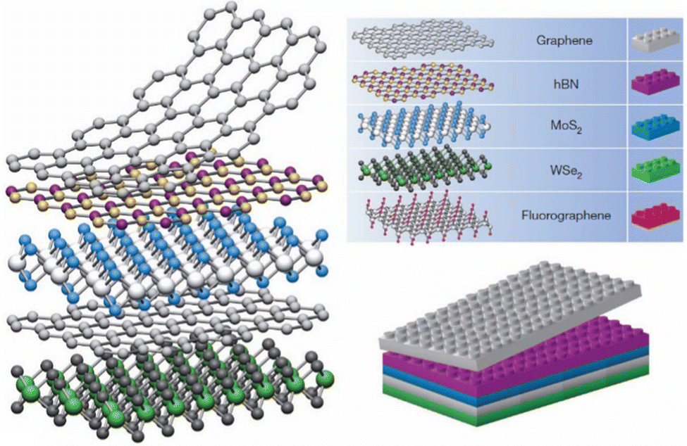 | ||
| Fig. 4 Building van der Waals heterostructures by combining different layers of 2D materials. Adapted from ref. 42. | ||
The group of pnictogens (P, As, Sb and Bi) exhibits several allotropes with layered structures, both with rhombohedral and orthorhombic structures.34 In this sense, true van der Waals forces held the layered assembly in the orthorhombic structure, while the interlayer interactions of the rhombohedral counterparts increase concomitantly with the atomic number, i.e., the nature of the pnictogen.53 The first one to be described was phosphorene in 2014, the 2D counterpart of layered black phosphorus, which exhibited great potential as a p-type semiconducting material (Fig. 5). The authors described a few-layer phosphorene field-effect transistor with a channel length of 1.0 μm at room temperature, which displayed a high on-current of 194 mA mm−1 together with a high hole field-effect mobility of 286 cm2 V−1 s−1 and an on/off ratio of up to 104.54 Phosphorene exhibits an orthorhombic crystalline form in which the P atoms are assembled composing hexagonal puckered layers that are sustained thanks to true van der Waals forces. It displays high reactivity as well as a rapid oxidation under ambient conditions leading to the formation of PxOy compounds which, in the presence of moisture, leads to the formation of phosphoric acid and related compounds.55 Furthermore, it has a modulable bandgap that ranges from 0.3 eV to 2.2 eV for bulk and monolayer black phosphorus, respectively.56 Since then, phosphorene has been extensively studied, including its exfoliation,57–59 its covalent and noncovalent functionalization55,60,61 as well as its different applications.55,62–65 Analogous 2D pnictogens (arsenene, antimonene and bismuthene) have been also predicted and most of them have been experimentally obtained.53,66
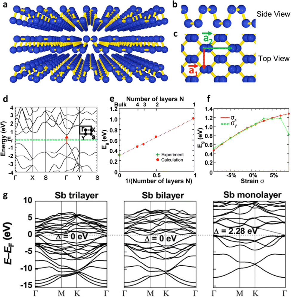 | ||
| Fig. 5 Crystal structure and band structure of few-layer phosphorene. (a) Perspective side view of few-layer phosphorene. (b) and (c) Side and top views of few-layer phosphorene. (d) Theoretical band structure of a phosphorene monolayer calculated using DFT-HSE06. (e) and (f) DFT-HSE06 results for the dependence of the energy gap in few-layer phosphorene on (e) the number of layers and (f) the strain along the x- and y-directions in a monolayer system. (g) Representation of the electronic band structures of antimony trilayers, bilayers, and monolayers calculated using DFT-HSE06. Adapted from ref. 54 with permission from American Chemical Society, copyright 2014 and ref. 76 with permission from John Wiley & Sons, copyright 2015. | ||
In this sense, it is important to point out that the -ene suffix in these materials (phosphorene, antimonene, bismuthene as well as others such as germanene or silicene) does not refer to a double bond between the individual atoms as in graphene. Nevertheless, these sorts of 2D materials composed of one single element are commonly referred to as Xenes by the scientific community.67 The layered structure of As corresponds to rhombohedral gray arsenic, and exhibits a tunable bandgap depending on the number of stacked layers of the material, ranging from a predicted 0.47 to 2.49 eV for a bilayer and a monolayer arrangement, respectively.68 Studies concerning arsenene are very scarce; nevertheless, there are some reports regarding the preparation of multilayer arsenene with a rhombohedral structure. For example, in the form of applying nitrogen plasma with indium arsenide, giving rise to the synthesis of multilayer arsenene nanoribbons on the surface of the InAs.69 Regarding heavy pnictogens (Sb & Bi), the fact of descending through the group implies an increase in interlayer interactions, going from being purely vdW materials to having a marked covalent character. Specifically, group 15 elements (without considering nitrogen) tend to favor the sp3 hybridization, but in their ns2 np3 valence configuration they tend to form layered structures showing in-plane covalent bonds together with weaker interlayer bonds, which are purely vdW in the case of phosphorene, but progressively incorporate interlayer orbital hybridization in heavier elements, thus forming quasi-vdW materials. This latter aspect is critical in the case of bismuth, thus precluding its micromechanical exfoliation. Moreover, the strong spin–orbit coupling characteristic of heavy pnictogens results in the fact that both known structures of bismuth (α and β forms) have been reported as topological insulators, with predicted bandgaps of 0.18 and 0.23 eV for the bilayer α and β forms, respectively, that increase to 0.30 and 0.32 eV for the monolayer α and β-bismuthene, respectively.70,71 There are reports of the successful synthesis of few-layer bismuthene via, for example, liquid phase exfoliation giving rise to few-layer systems; however, the strong tendency to oxidation of this material usually leads to heavily oxidized systems with poor morphologies.72,73 Hence, recent studies on top-down bismuthene materials reveal promising results in energy storage (i.e. sodium- and potassium-ion batteries), electrocatalysis such as selectively catalyzing the electroreduction of CO2 to HCOO−, or photonics.73 Moreover, wet-chemical approaches have been reported involving thermal reduction or hot-injection reactions leading to 2D bismuth with different morphologies and degrees of oxidation.74,75
Taking all this information into account, antimonene holds a privileged position in group 15 because despite being a heavy pnictogen, it still maintains a marked van der Waals character in its interlaminar interactions. This intermediate position allows us to exploit not only the physical applications of antimonene (e.g. optical or electronic) but also its pronounced chemical reactivity, of extreme importance in applications beyond electronics, such as biomedicine, sensing, energy or catalysis. In this review we will particularly focus on antimonene; we will give an overall view of the history and properties, later on we will thoroughly analyze the different synthetic methodologies and characterization techniques. We will also tackle the latest insights on chemical reactivity, including oxidation behavior and chemical functionalization, to finally address all potential applications reported so far for this brand-new material.
2. General physical and chemical properties of antimonene
2.1 History of antimonene: from the theoretical predictions to its experimental isolation
The story of antimonene begins in 2015 when Zhang et al. theoretically identified using density functional theory (DFT) the existence of novel 2D layered materials composed of Sb and As monolayers, which were labelled as antimonene and arsenene, respectively. These predictions anticipated that both materials would display good stability, high carrier mobility as well as a wide range of bandgaps according to the total number of layers.76 That work showed that although Sb and As are mostly semi-metallic elements in bulk, they are both transformed into indirect semiconductors, highlighting a bandgap of 2.28 and 2.49 eV when thinned to the monolayer region (Fig. 5). In addition, antimonene and arsenene evolve from indirect semiconductors to direct bandgap semiconductors if a small biaxial strain is applied, exhibiting great potential for optoelectronic applications. In the modelling a buckled honeycomb structure was also predicted where each atom is bonded to three adjacent atoms of the same layer achieving octet stability. This arrangement is similar to those observed for germanene and silicene and thus aids in the stabilization of the layered structure.77Fig. 5(g) presents the original electronic band structure of antimony trilayers, bilayers and monolayers (calculated at the HSE06 level of theory) as presented by Zhang et al.76After this initial study, numerous articles dealing with various theoretical aspects of antimonene appeared, pinpointing the interest of different properties of the material and postulating several potential applications.35,78–80 For instance, the studies by Karna and co-workers exhibited that free-standing α and β allotropes of antimonene are stable and semiconducting.35 In this sense, while the α form has a puckered structure with two atomic sublayers, the β allotrope displays a buckled hexagonal lattice. Another interesting difference between both allotropes is the strong anisotropy of the α form which contrasts with the nearly isotropic mechanical properties of β-Sb. The possibility of the existence of additional allotropes (γ and δ) was also investigated, concluding in the structural instability of both of them compared with the α and β forms. The parameter chosen for analyzing the stability was the phonon dispersion curves, displaying no imaginary vibrating modes for the α and β allotropes, hence implying their stability as free-standing monolayers, a point additionally supported by using several exchange and correlational functional forms of DFT.35 In contrast, γ and δ forms did exhibit imaginary vibrational modes, thus confirming their structural instability. This work also conveyed that a moderate tensile strain would induce a transformation from indirect to direct bandgap transition in antimonene, as well as a marked vibrational Raman bands that can be very useful in the characterization of monolayers. Fig. 6 presents, on the one hand, the structural configuration of antimonene allotropes, and, on the other hand, the predicted electronic properties of α and β allotropes. Interestingly, allotropic forms of antimonene have been experimentally investigated in the formation of van der Waals heterostructures, where it has been found that the rhombohedral β phase is the most stable,81–83 but the orthorhombic α-phase can be metastable at the few-layer regime, showing a spontaneous transition from the orthorhombic to the rhombohedral bulk-like phase for thicknesses beyond 4 nm.82
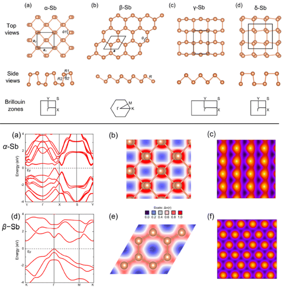 | ||
| Fig. 6 Top: Structural configurations of antimonene allotropes: (a) α-Sb, (b) β-Sb, (c) γ-Sb, and (d) δ-Sb. Bottom: Electronic properties of (a)–(c) α-Sb and (d)–(f) β-Sb monolayers: (a), (d) band structure, (b), (e) charge density projected in the plane, and (c), (f) simulated scanning tunneling microscopy (STM) images. Adapted from ref. 35 with permission from American Chemical Society, copyright 2015. | ||
In 2016, Ares et al. were the first to obtain and experimentally isolate antimonene.84 In this work, the micromechanical exfoliation of bulk crystals of Sb was carried out down to the single-layer regime, showing experimental evidence of the stability of antimonene under ambient conditions. Furthermore, the provided experimental data highlighting good stability and no degradation for months. Moreover, additional DFT simulations mimicked ambient conditions and confirmed the experimental results, predicting a bandgap of 1.2–1.3 eV corresponding to an interesting range of optoelectronics applications. Fig. 7 shows evidence of experimental antimonene flakes obtained by micromechanical exfoliation on SiO2 substrates.
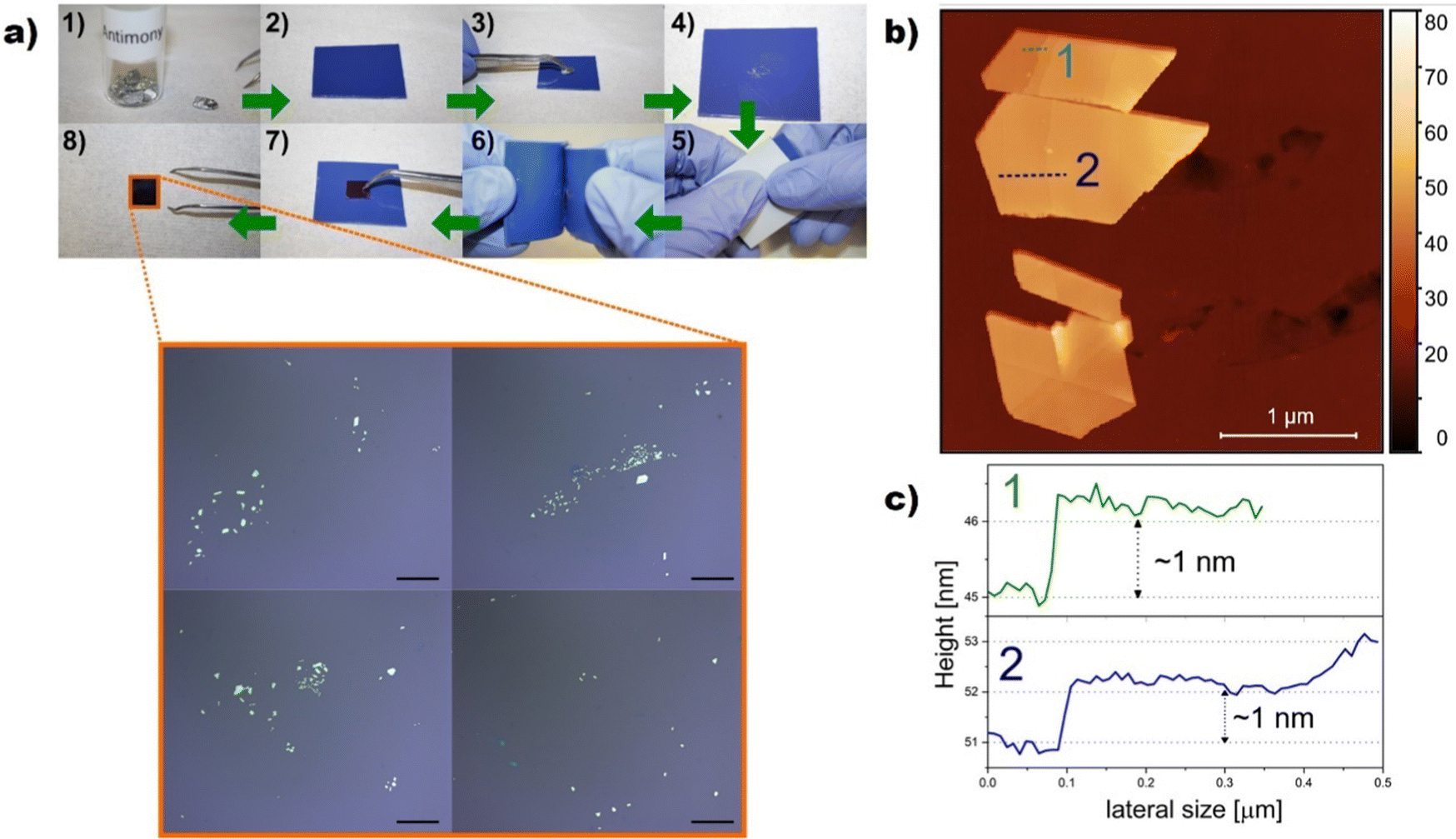 | ||
| Fig. 7 (a) Step-by-step procedure (1–8) for the exfoliation of ANSs using micromechanical approach. Inset in (8) Optical micrographs showing exfoliated ANSs with different polygonal geometries. Scale bars 20 μm. (b) AFM image of typical ANSs and (c) height profiles along the dashed lines showing steps of approximately 1 nm, compatible with a single layer antimonene. Adapted from ref. 98 with permission from IOP Publishing, copyright 2020. | ||
Transmission electron microscopy (TEM) of antimonene flakes confirmed a clear hexagonal periodicity as expected for the few-layer β-Sb phase. Regarding the feasibility of achieving a single-layer of antimonene, a monolayer terrace was observed with a height of ca. 0.9 nm that surely included additional water molecules. It is widely assumed that this layer of adsorbed water molecules is always present under ambient conditions, with an average thickness of ca. 0.6 nm which is present between the deposited flakes of the material and the SiO2 substrate.85,86 These pioneering studies paved the way for the development of the chemistry and physics of antimonene. Henceforth, hundreds of papers dealing with different aspects of antimonene have been published, corroborating the interest generated by this novel 2D material (Fig. 3).
2.2 Properties
Antimonene has been proposed as a good candidate for novel applications due to its outstanding properties. Nevertheless, one has to take into account that some of them have not been experimentally tested yet; therefore, the main properties of the material are a combination of the actual experimental and theoretical results as reviewed below:Nevertheless, the study of antimonene heterostructures revealed the plasticity of this novel material, the structure of which is critically dependent on its surroundings. This includes thickness driven phase transitions and substrate-layer stability dependence.82,83 This rich allotropic dynamism generates a wide number of possible antimonene structures with unique properties that can be exploited specifically to meet the requirements of each application.
Moreover, with plasmon energies of ca. 9 eV, the combination of the dielectric function and electron energy loss spectroscopy (EELS) reveals sections of the electromagnetic spectrum where antimonene behaves as a metal.88 Recent studies confirm these results and the applicability in optoelectronics.92 The authors remark the significant absorption from the visible to the ultraviolet region of α-antimonene that can be, thus, used as an adequate saturable absorber, while the β form displays an almost negligible absorption in the visible region.92
Electrical transport in this material has also been recently studied, concluding that antimonene is expected to exhibit unusual transport properties due to its topological phase transition feature and quantum spin Hall edge states.93 These intrinsically localized edge channels oriented to electrical transport can be controlled by applying an external electric field.93
Furthermore, Ares et al. studied the morphological and electronic properties of micromechanically exfoliated antimonene, from single layer to few-layer regime.94 They observed that the conductance of the antimonene sheet was constant with the number of layers, obtaining a carrier concentration similar to graphene under ambient conditions, and thus having a resistivity independent of the flake thickness (1200 Ω sq−1) larger than that observed for graphene. The experimental measurements along with theoretical calculations suggest that the topologically protected surface states play a key role in antimonene electrical properties.
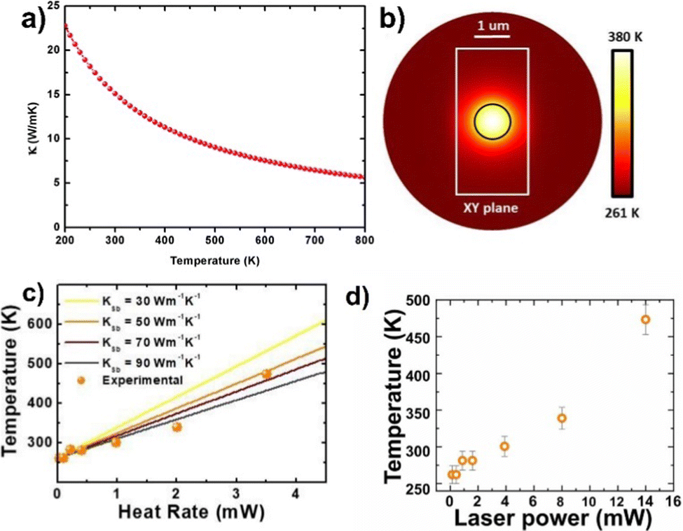 | ||
| Fig. 8 (a) The lattice thermal conductivity of antimonene as a function of temperature. (b) Zenith view of the temperature mapping for a rectangular flake (white lines) considering a disk-like heat source (black circle). (c) Average temperature of the excitation spot as a function of the heat source rate for different thermal conductivities of the flake. (d) Temperature of the probed ANS as a function of laser power, estimated using both calculated power and temperature coefficients. Adapted from ref. 95 with permission from Royal Society of Chemistry, copyright 2016, and ref. 98 with permission from IOP Publishing, copyright 2020. | ||
Furthermore, the electronic and magnetic properties can be additionally modified by applying in-plane biaxial strains. When this strain is above 4%, the ferromagnetic half-metal nature will evolve into an antiferromagnetic semiconductor with no change in the total magnetic moment. Similarly, small compressive strains can reduce the magnetic response giving rise to an n-type doping semiconductive state at a strain of −4%. Regarding the amount of vacancy, a high number of these could even quench the induced magnetism.99 These tunable magnetic response set antimonene as a good candidate towards the development of new low-dimensional spintronic devices.100 With respect to the doping of the Sb layer with transition metals such as Cr, V, Ti or Fe, to name a few, the predicted influence on the magnetic behaviour diverges according to the chosen metal.101 For example, Cr-doped systems transform the magnetic semiconductor nature to a magnetic half-metal material after applying a biaxial tensile strain of 6%.
Also, the bandgap closing can be achieved under a biaxial strain between −4 to −6%, resulting in metallic features. The tensile strain also increases the local magnetic moments up to ca. 5.00 μB compared with the unstrained system.102 Fe-doped systems can lead to stable room temperature ferromagnetism, combined with a strong orbital hybridization (p–d) and a spin–orbit coupling effect which results in a significant spin splitting around the Fermi level. Introducing V atoms into an Fe-doped system changes the overall magnetic order from ferromagnetic to antiferromagnetic.103 In this line, the structural and mechanical properties of antimonene monolayers doped with transition metals such as Sc, Ti, V, Cr, Fe, Co, Ni, Cu, and Zn have also been theoretically addressed via DFT calculations.104 The study pointed out a reduction in the yield strain of the nanosheets under biaxial loading, resulting in the reduction of the Young's and bulk moduli. Overall, these results pinpoint strain and defect engineering as promising routes for the modulation of the magnetic behavior in antimonene.
Second, antimonene alloys have also been recently reported in different studies. For example, López-Marzo et al. demonstrated that 2D Sb2Te3 is suitable for optoelectronics and thermoelectric applications.107 The antimony alloy was synthesized after putting the appropriate stoichiometric amount of Sb and Te in a quartz glass ampoule under high vacuum and posterior heating in the absence of air. Specifically, the few-layer and micrometer-sized Sb2Te3 was obtained after a glove box-free electrochemical exfoliation of the as-synthesized bulk material in Na2SO4, which resulted in high yields and good stability. In this context, it is worth noting that the inherent oxidation of the alloy surface can be tuned by switching the voltage polarity during the exfoliation procedure. Antimonene alloys with arsenic can be found in different studies in the literature.108–110 2D AsxSb1−x (previously predicted by DFT109,110) was experimentally grown via molecular beam epitaxy giving rise to a stable alloy under ambient conditions on Si, Ge or graphene substrates.108 It was found that As composition can be tuned up to 15% using this co-deposition approach. The synthesis of new Sb alloys widens the scope of feasible applications towards new tunable devices. Further important reactivity aspects such as surface oxidation or functionalization will be thoroughly discussed in the following sections.
3. Synthetic approaches in the preparation of antimonene and its heterostructures
When producing 2D materials, including antimonene, it is crucial to have control over the thickness (i.e. number of layers), lateral dimensions, crystallinity or surface features in order to systematically study the properties of the material as well as point towards their specific applications. In broad strokes, one can divide the methods of synthesizing antimonene into two different groups: top-down and bottom-up approaches, as summarized in Fig. 9.113,114 Top-down refers to using exfoliation tools that are controlled by external forces like electrochemical potential, ultrasound or shear forces, to create nanoscale structures starting from bulk crystals and reducing them to the desired size, shape and features. In stark contrast, bottom-up approaches are based on using atomic or molecular components as building blocks for the direct self-assembly via specific reaction mechanisms, yielding 2D materials that can be prepared either free-standing or supported on surfaces.113,115,116 This strategy has allowed the preparation of the first antimonene-based heterostructures with other 2D materials like graphene, allowing the elucidation of the interface properties and several aspects related to the rich allotropic/polymorphic structural diversity. In the case of antimonene, both approaches have been reported in the literature and we will detail each of them below.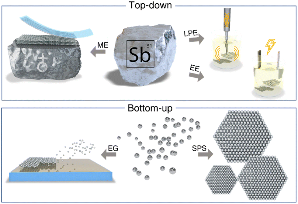 | ||
| Fig. 9 Main synthetic approaches in the synthesis of antimonene classified in top-down and bottom-up approaches. Acronyms stand for mechanical exfoliation (ME), liquid phase exfoliation (LPE), electrochemical exfoliation (EE), epitaxial growth (EG) and solution-phase synthesis (SPS). | ||
3.1 Top-down approaches
The as-obtained micrometric-flakes were then easily identified by means of optical microscopy. Then, AFM images depicted an average height of ca. 0.9 nm for a monolayer terrace at the bottom of a few-layer antimonene flake (Fig. 10). As previously commented, the 0.9 nm value takes into account the existence of water molecules trapped between the flake and the SiO2 substrate.85,86 Nevertheless, statistics has to be taken into account when talking about AFM thicknesses. The mechanical stability of the monolayer terrace was also confirmed after folding it with no breakage by AFM-assisted nanomanipulation. Additional techniques such as high-resolution transmission electron microscopy (HRTEM) and X-ray energy dispersive spectroscopy (XEDS) in combination with high-resolution AFM confirmed the quality of the material and its rhombohedral structure, that is, corresponding to β-antimonene. Finally, the stability of the material under ambient conditions as a function of time (up to two months) was also studied. It was observed that not only is antimonene stable after that time but also is after the immersion of the sample in water, thus depicting the high overall stability of the material in the presence of moisture (the role exerted by surface oxidation will be discussed later, vide infra).84
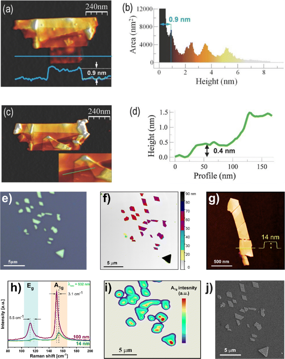 | ||
| Fig. 10 AFM topography images of an antimonene flake with a monolayer terrace at the bottom. (a) AFM topography showing an antimonene flake with terraces of different heights. (b) Height histogram of the image in (a) pointing out the different thicknesses of the terraces. (c) Same flake as in (a) after a nanomanipulation process to confirm the stability of the material. The lower terrace of the flake was folded upward resulting in an origami structure with different folds. The inset corresponds to the area of the origami where the lowest step height is found. (d) Profile along the green line in the inset in (c). (e) Optical micrograph of a typical antimonene nanosheet isolated on SiO2/Si substrate using micromechanical exfoliation. (f) False-colored AFM image of the same ANSs with incremental color code to highlight the terraces. Each color indicates a 10 nm step (g) AFM image of a few-layer antimonene nanosheet and height profile along the dashed yellow line. (h) Comparative Raman spectra of the pristine bulk (100 nm) and few-layer (14 nm) antimonene nanosheets, remarking the blue shift of the of A1g and Eg modes for the few-layer antimonene nanosheets. (i) Scanning Raman microscopy (SRM) map of the intensity of A1g mode of the flakes in (e). (j) Scanning electron microscope (SEM) image of the same flakes in (e). Adapted from ref. 84 with permission from John Wiley & Sons, copyright 2016, and ref. 98 with permission from IOP Publishing, copyright 2020. | ||
Recently, our group managed to introduce a deterministic method to easily isolate antimonene nanosheets (ANSs) through an adapted micromechanical exfoliation approach using a high-tack adhesive film.98 Indeed, we have been able to isolate ANSs exhibiting well-defined polygonal shapes with smooth surfaces and sharp edges (Fig. 10(e) and (j)) in very high density over the SiO2/Si substrate. Topographic analysis using AFM revealed ANSs in a few-layer regime with thicknesses down to 14 nm (Fig. 10(f) and (g)). Moreover, the Raman spectra of the thin flakes displayed a noticeable blue-shift due to the strong electron–lattice interaction resulting from the reduced stacking order, which falls perfectly in line with previous theoretical predictions (Fig. 10(h)).117 Furthermore, we have been able to demonstrate a perfect correlation using four different analytical techniques, namely optical microscopy, AFM, scanning Raman microscopy (SRM) and scanning electron microscopy (Fig. 10(e), (f), (i) and (j)), respectively. This neat correlation allowed for the simultaneous and at the same time unambiguous identification of the morphology and the chemical structure of the probed sample. It is worth noting that such correlations are of critical importance in the characterization of 2D materials, and the reliance on individual measurements in distinct locations, even within the same sample, can be dangerously misleading, especially for new and not well understood systems such as the case of antimonene. It is commonplace to encounter washing solvent residues or impurities from the polymer used for delamination exhibiting flat morphologies, which might be erroneously identified as antimonene flakes if solely measured by AFM without a direct correlation to other techniques, such as Raman for instance.
The main limitation of this micromechanical approach is that it yields a low quantity of exfoliated material, highlighting the need for alternative methods to develop antimonene on a large scale.
:1) suspensions of few-layer antimonene starting from bulk Sb crystals. Afterwards, the non-exfoliated material was removed by cascade centrifugation at 3000 rpm To do this, the LPE process is carried out with tip sonication avoiding additional stabilizers such as surfactants. The high quality of the nanosheets was unveiled with AFM, scanning electron microscopy (SEM), Raman spectroscopy or EELS. AFM on SiO2 substrates revealed step heights of 4 nm, related to the presence of few-layer material (Fig. 11). This value considers the overestimation because of residual solvent or additional contributions such as adhesion and capillary forces.59,122,123 The overall lateral dimensions were found to be in the 1–3 μm range and the atomic periodicity indicates a β-phase. Additionally, the obtained nanolayers were extremely stable under ambient conditions. Regarding the Raman characterization, the correlation of statistical Raman microscopy (SRM) with AFM in a polydisperse sample revealed antimonene flakes with thicknesses below 70 nm, corresponding to 17 layers, and barely showing any Raman signal. This result was similar to that observed for micromechanically exfoliated flakes.84
 | ||
| Fig. 11 (a) TEM image of FL antimonene nanolayers. (b) Representative topographic AFM image (scale bar 2 μm) of the exfoliated FL antimonene nanolayers. (c) Corresponding Raman A1g map (scale bar 2 μm) of the exfoliated FL antimonene nanolayers contained in the area dotted in white in (b). (d) AFM image of typical ANS showing polydisperse nanosheets exfoliated by ultrasonication. (e) Statistical dispersion of ANS lateral size as a function of thickness. (f) Thickness measured by AFM along the lines numbered in (d). Adapted from ref. 112 with permission from Royal Society of Chemistry, copyright 2019, and ref. 125 with permission from IOP Publishing, copyright 2020. | ||
After this initial work back in 2016, LPE is commonly being used as a methodology to obtain antimonene.112,124,125 Since then, great effort has been made to maximize the concentration of the samples obtained by LPE, while maintaining an appropriate “dimensional anisotropy” (DA) ratio, which has been defined as the ratio between the height and length of the nanolayers, providing a good estimation of the morphology of the nanolayers (having the thin and large flakes a high DA ratio). We have reported a systematic study of the exfoliation process of antimony bulk crystals, with the aim to obtain stable FL antimonene suspensions with a high nanolayer concentration as well as a high DA ratio, by optimizing different parameters of the exfoliation procedure.112 Specifically, the results show that the pre-processing of the material using wet-ball milling with 2-butanol strongly affects both the concentration and morphology of the suspension of FL antimonene. Moreover, the analysis of 28 different solvents previously selected based on Hansen parameters as well as other experimental observations yielded the highest concentration of FL antimonene for the mixture of NMP/H2O in a (4:1) ratio, ca. 0.368 g L−1 (∼yield of 37 wt%), while the largest DA value was obtained using 2-butanol (ca. 27.6). The nanolayer heights was comprised between 2 and 8 nm and lateral dimensions lower than ca. 300 nm. Additionally, this work revealed that using tip sonication employing an ultrasonic wave amplitude of 100% yields better results in terms of DA than bath sonication. Interestingly, the use of 2-butanol also yielded a large number of edges and electroactive sites that strongly influence the electrochemical behavior of the exfoliated antimonene, forming also irreversible superficial antimony oxides.112
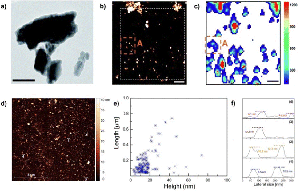
A particular case within the LPE is that of the antimonene quantum dots (AMQD). This type of material – of great interest in biomedical applications (vide infra) – which is characterized by lateral dimensions <8 nm, is obtained after subjecting the bulk antimony samples to an iterative sonication and centrifugation process for long periods of time using high power and high amplitude values.126,127 More in detail, this procedure combines ultrasound tip sonication with ice bath sonication of bulk Sb in NMP or ethanol, followed by a low-speed centrifugation to remove the larger particles and a high-speed centrifugation to isolate the desired QD particles. Fig. 12 highlights the synthesis and characterization of AMQDs in EtOH according to ref. 127. The resulting solution displays a high yield in the synthesis of uniform and small particles with average size and thickness of ca. 3 and 2 nm, respectively, as detected by AFM, in good agreement with TEM images. The composition of the AMQDs and the presence of Sb was determined via XPS and Raman spectroscopy. Moreover, in order to improve their biocompatibility, a non-covalent functionalization with polyethylene glycol (PEG) moieties has been carried out.
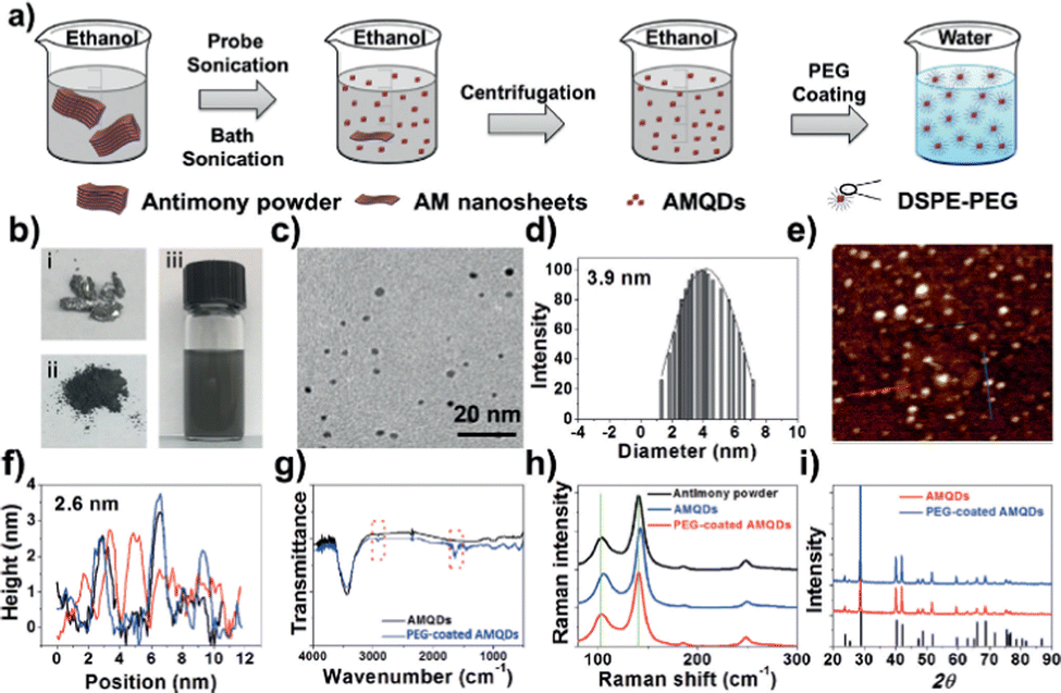 | ||
| Fig. 12 (a) Fabrication of PEG-coated AMQDs. (b) Images of bulk antimony, antimony powder, and AMQD solution during the preparation process. (c) TEM image, (d) diameter distribution, (e) AFM image, and (f) thickness of the PEG-coated AMQDs. (g) FTIR spectrum, (h) Raman spectrum, and (i) XRD spectrum of AMQDs and PEG-coated AMQDs. Reproduced from ref. 127 with permission from John Wiley & Sons, copyright 2017. | ||
The as-obtained PEG-coated AMQDs exhibited excellent stability in physiological experiments; no signs of toxicity in cells in the studied range of concentrations and excellent photothermal conversion efficiency upon NIR irradiation. Beyond the biomedical applications,127 recent studies on AMQDs points to them as promising candidates in optoelectronic devices, and more specifically in quantum-dot-sensitized solar cells.128,129 In this sense, the work of Zhang et al.129 presents liquid phase-synthesized AMQDs as an effective photoactive material in quantum-dot-sensitized solar cells. The AMQDs were prepared following the aforementioned protocol starting from bulk Sb crystals using a simple probe ultrasonic procedure followed by an ultrasound bath treatment. The temperature during the probe sonication was set under 25 °C to avoid possible oxidation or degradation processes. Afterwards, the dispersion was centrifuged to remove the residual Sb bulk particles and the resulting suspension was centrifuged at high speed (12000 rpm) to collect the supernatant AMQDs, which were re-suspended in NMP. AFM revealed an average thickness of ca. 2.2 nm and the related Sb Raman bands A1g and Eg modes confirmed the nature of the QDs. The combination of the AMQDs with strong light–matter interaction, moderate energy bandgap in the visible range and antioxidation properties allows a photoelectric conversion efficiency up to 3.07%, alongside the long-term stability of these quantum-dot-sensitized solar cells (more than 90% of the initial conversion efficiency after 1000 h).
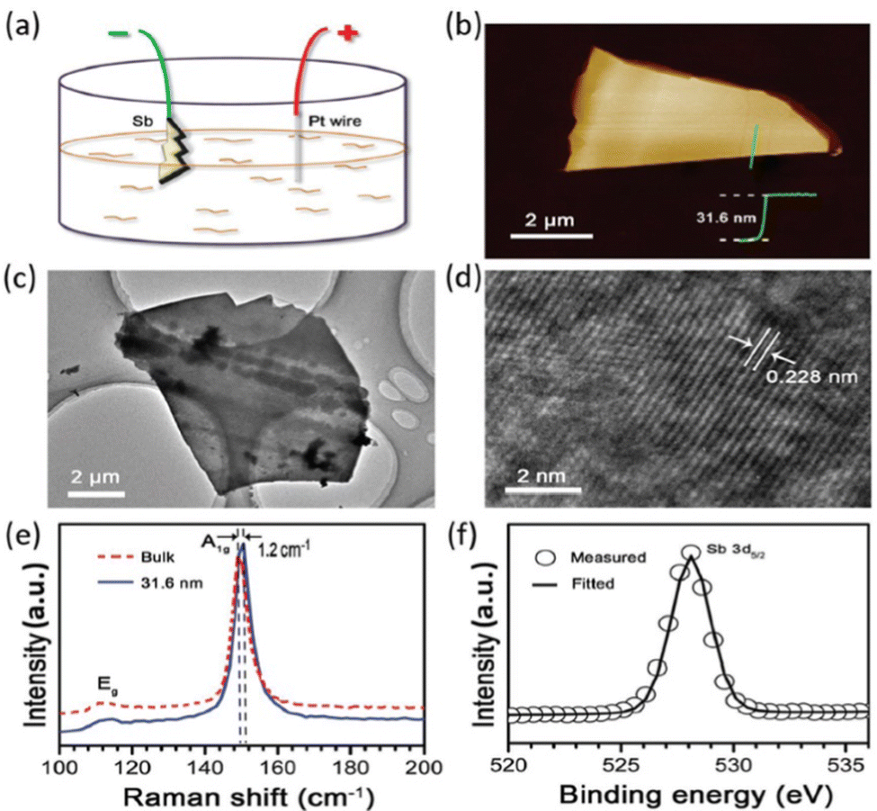 | ||
| Fig. 13 Characterization of the prepared multilayer antimonene by electrochemical exfoliation. (a) Schematic illustration of the two-electrode system used for the procedure, depicting bulk Sb, Pt wire, and Na2SO4 aqueous solution as the working electrode, counter electrode, and electrolyte, respectively. (b) AFM image of a multilayer antimonene nanoflake obtained by electrochemical exfoliation. (c), (d) TEM and HRTEM images of the electrochemical exfoliated antimonene. (e) Raman spectra of the bulk antimony and multilayer antimonene shown in (b). (f) XPS spectrum showing the Sb 3d5/2 peak of the exfoliated multilayer antimonene. Reproduced from ref. 126 with permission from John Wiley & Sons, copyright 2017. | ||
The ability to intercalate alkali metals shown by Sb allows the formation of antimony intercalation compounds to be envisioned, in analogy to previously reported black phosphorus intercalation compounds (BPICs), which under appropriate solvents and under thorough exclusion of oxygen and water may lead to pnictogenide dispersions.61,134–136
3.2 Bottom-up approaches
The MBE approach was previously carried out by Lei et al. with the growth of single layer Bi (111) on Bi2Te3 (111) and Bi2Te3 (111) substrates with a small lattice mismatch.139 Afterwards, Wu et al. were able to grow antimonene monolayers (thickness of ca. 0.28 nm as measured by the profile line across the edge of the antimonene film) on PdTe2 substrates (Fig. 14).140 In that work, both in situ low-energy electron diffraction (LEED) and scanning tunneling microscopy (STM) measurements confirmed the high quality of the epitaxially-grown antimonene with a honeycomb graphene-like structure. XPS results reported that the interaction between antimonene and the substrate is via weak van der Waals forces. The combined results of STM and XPS highlighted a good stability of the material against air exposure for 20 min.
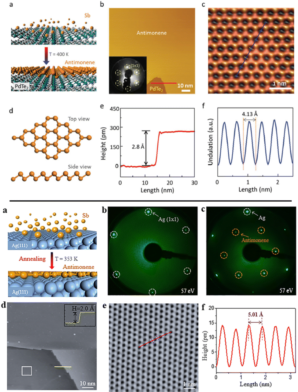 | ||
| Fig. 14 Top: (a) Schematic of fabrication of an antimonene monolayer formed on the PdTe2 substrate obtained by MBE approach. (b) STM topographic image of large antimonene island on PdTe2. (Inset: LEED pattern of antimonene on PdTe2.) (c) Atomic resolution STM image of monolayer antimonene showing the graphene-like honeycomb structure. (d) Top view and side view of the buckled conformation of the antimonene honeycomb. (e) Height profile along the red line in (b), showing that the apparent height of the antimonene island is 2.8 Å. (f) Line profile corresponding to the blue line in (c), revealing the periodicity of the antimonene lattice (4.13 ± 0.02 Å). Bottom: (a) Schematic of the MBE fabrication process. (b) LEED pattern of a clean Ag(111) substrate. (c) LEED pattern of antimonene on Ag(111). (d) Large scale STM image of monolayer antimonene on the Ag(111) (inset: height profile along the yellow line at the terrace edge). (e) High-resolution STM image of antimonene depicted by the white square in (d). (f) Line profile corresponding to the red line in (e), revealing the periodicity of the antimonene lattice (5.01 Å). Adapted from ref. 140 with permission from John Wiley & Sons, copyright 2016, and ref. 141 with permission from American Chemical Society, copyright 2018. | ||
Most recently, additional studies have used MBE to grow antimonene on Ge (111) and Ag (111) (Fig. 14) substrates, confirming the weak interactions between the monolayer and the substrate as well as the honeycomb structure.81,141 Moreover, these studies revealed a semi metallic behavior for a single layer of deposited antimonene. MBE has also been reported to obtain multilayer antimonene nanoribbons on sapphire substrates that can extend themselves to a length of few microns.36 These ribbons were grown via in situ thermal annealing after the initial MBE deposition. Their formation mechanism, supported on SEM and AFM measurements, considers an adatom migration process at an elevated temperature in combination with strain relaxation and surface energy balance.
vdWE is based on the use of substrates with the absence of dangling bonds on their surface. Thus, the epitaxially grown layer of the layered material is connected to the substrate by means of weak van der Waals interactions in the absence of strong chemical bonds. Therefore, it is possible for the material to exhibit a different crystalline symmetry than that of the substrate. The first few-layer antimonene grown by vdWE was reported in 2016 by Ji et al.117Fig. 15 highlights the antimonene layer synthesized on mica substrates by means of a van der Waals epitaxy.
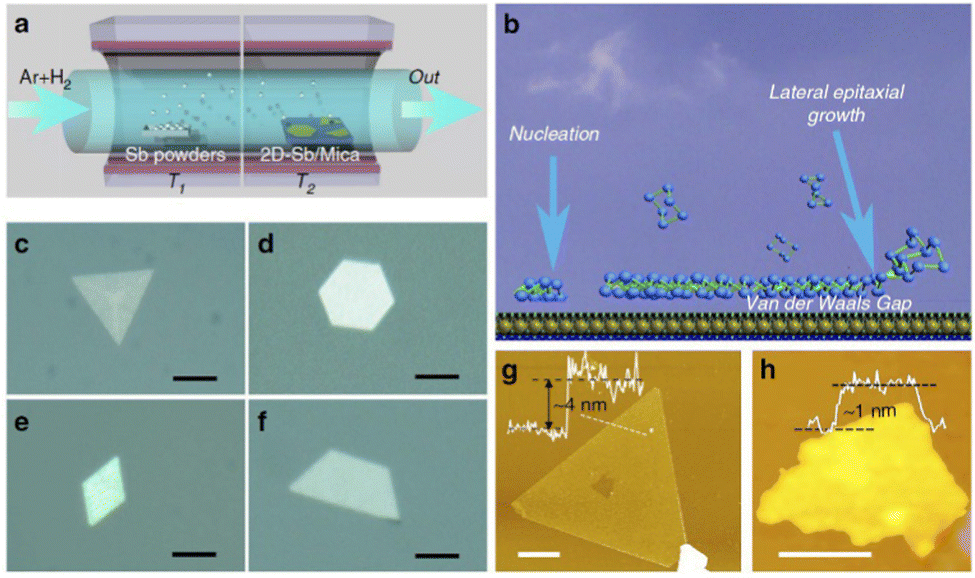 | ||
| Fig. 15 Antimonene synthesized on mica substrates via vdW epitaxy. (a) Schematic illustration of the sample synthesis configurations. (b) Schematic diagram of the vdWE. (c)–(f) Optical images of typical antimonene polygons with triangular, hexagonal, rhombic, and trapezoidal shapes, respectively. The scale bar is 5 mm. (g) AFM image of a typical triangular antimonene sheet. The scale bar is 1 mm. (h) AFM image of a tiny antimonene sheet with a thickness of ca. 1 nm. The scale bar is 50 nm. Reproduced from ref. 117 with permission from Springer Nature, copyright 2016. | ||
In that work the high-quality synthesis of few-layer antimonene with a buckled hexagonal structure (β-phase) was reported as confirmed by HRTEM and Raman spectroscopy. This finding is consistent with the predicted as most stable allotrope of monolayered antimonene. In broad strokes, the synthesis is carried out in a two-zone tube furnace with separated temperature controls. The bulk Sb is placed in one of the regions and then heated to obtain Sb vapor. A transport flow of Ar + H2 transfers the Sb vapor to the other region of the furnace, in which there is a substrate at a lower temperature than the first region, hence promoting the condensation of Sb. The high stability of the material and an average dimension (5–10 μm) and thicknesses (ca. 4 nm, i.e., few-layers) were analysed by optical microscopy, AFM, Raman spectroscopy and XPS. The stability of the nanosheets was tested with an as-prepared and a 30 day aging sample, with no additional signature in the corresponding Raman spectra or X-ray energy-dispersive spectroscopy (XEDS). The good electrical conductivity of the synthesized antimonene (104 S m−1) in combination with the wavelength independent high transparency in the visible light spectrum endows this material with potential applications as a flexible transparent electrode.117
Along this front, Hogan et al. reported the temperature-induced phase transition between α and β phases of antimonene in a van der Waals heterostructure on Bi2Se3.142 The Bi2Se3 surface was prepared via an ultra-high vacuum chamber, and the antimony was then sublimated and deposited at room temperature. Once antimony is deposited, it forms α-antimonene domains with different orientations with respect to the substrate. However, after mild annealing at 473 K, there is a growing of the β phase that overcomes α-antimonene, leading finally to a single domain of β-antimonene which exactly matches with the surface lattice structure of Bi2Se3. These results were also supported by DFT calculations, which highlight the lattice matching of the β in stark contrast with the α one.
Last but not least, recent studies using vdWE have demonstrated the experimental synthesis of antimonene-based vdW heterostructures, proving the stability of both the hexagonal β- and rectangular α-forms of antimonene, on top of the topological insulator α-bismuthene.143 Moreover, these studies have allowed the elucidation of the rich allotropic/polymorphic structural diversity of antimonene, revealing extremely interesting rotational vdW epitaxy in 2D Sb/graphene heterostructures. Furthermore, thanks to these novel heterostructures several aspects related to the dynamic oxidation and phase transition of antimonene have been corroborated. These interesting points will be further analyzed below.
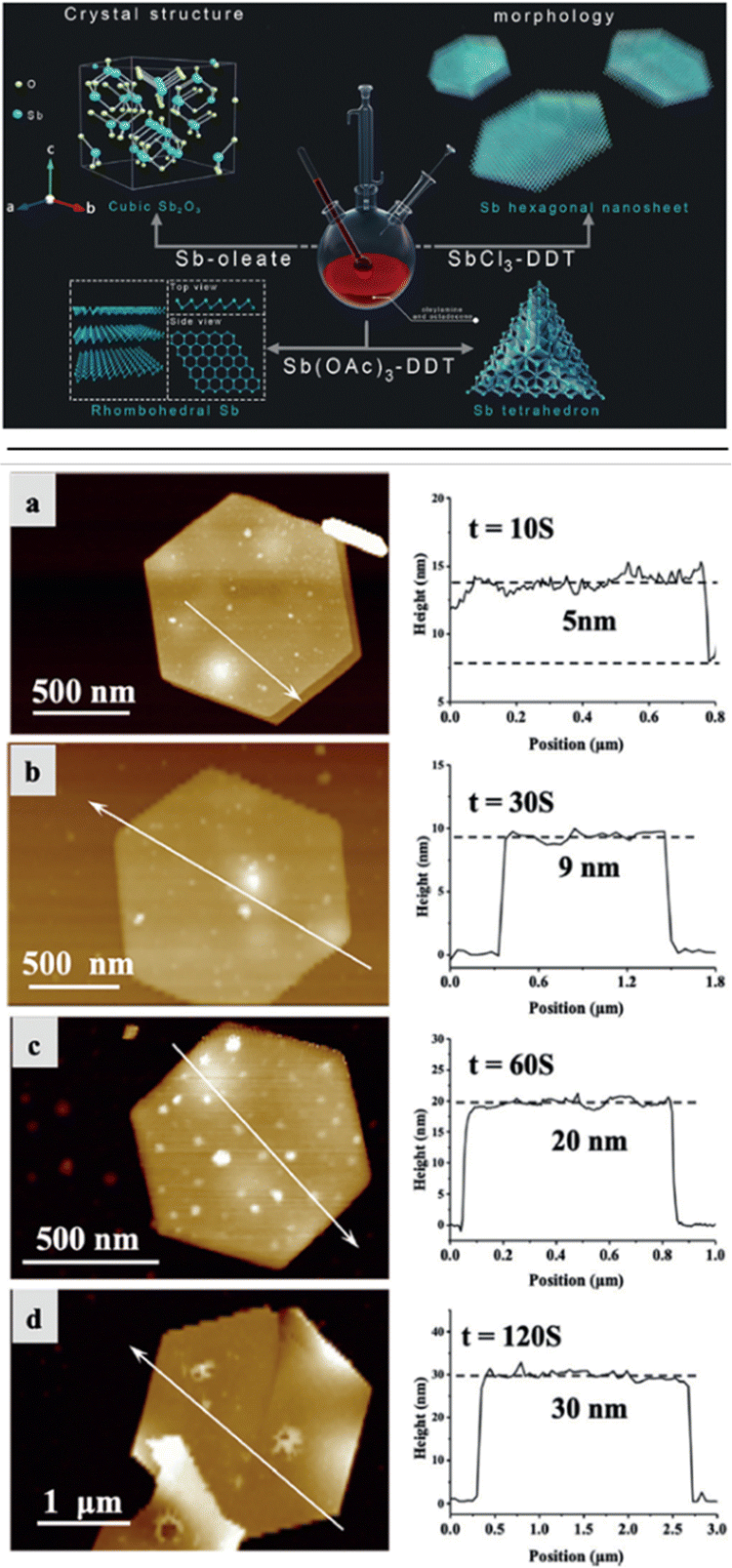 | ||
| Fig. 16 Top: Illustration of the wet chemical solution-phase synthesis of antimony trioxide, antimony tetrahedral, and hexagonal antimonene nanosheets from Sb-oleate, Sb(OAc)3-DDT, and SbCl3-DDT as precursors, respectively. Bottom: AFM images and the corresponding height profiles of hexagonal antimonene nanosheets with tunable layer thicknesses obtained at different annealing times at 300 °C: (a) 10 s, (b) 30 s, (c) 60 s, and (d) 120 s. Reproduced from ref. 144 with permission from John Wiley & Sons, copyright 2019. | ||
Some of the advantages of the solution-phase methodologies rely on their simple procedures, together with the tunability of the material from the point of view of size, morphology and composition, as well as the monodisperse character of the obtained samples,146,147 opening the door to the large-scale synthesis of the desired material. Indeed, the authors modulated to some extent the average thickness of the nanosheets by tuning the annealing time. They characterized the nanosheets via Raman spectroscopy, TEM and XRD proving that the material consisted of β-antimonene. Furthermore, X-ray photoelectron spectroscopy (XPS) results confirmed the presence of chloride anions on the surface of the antimonene, as well as the coordination of dodecanothiol, thus suggesting surface functionalization.
Furthermore, the colloidal synthesis of antimonene has been very recently studied by Abellán, Zamora and co-workers, optimizing the different synthetic parameters to obtain high-quality, ultrathin antimonene hexagons (Fig. 17).148 By studying the effects of each synthetic parameter on the resulting antimonene hexagons, like the precursor solution and the amount of volume injected, the antimony salt used, the hot-injection temperature or the reaction time, the authors have been able to gain control over the particle morphology. This further encouraged them to develop a scale-up process, which is essential for the real application of antimonene. For this, they have developed a continuous-flow synthesis reactor that allows the large-scale production of excellent morphological and structural quality antimonene hexagons, producing up to 0.964 mg h−1.
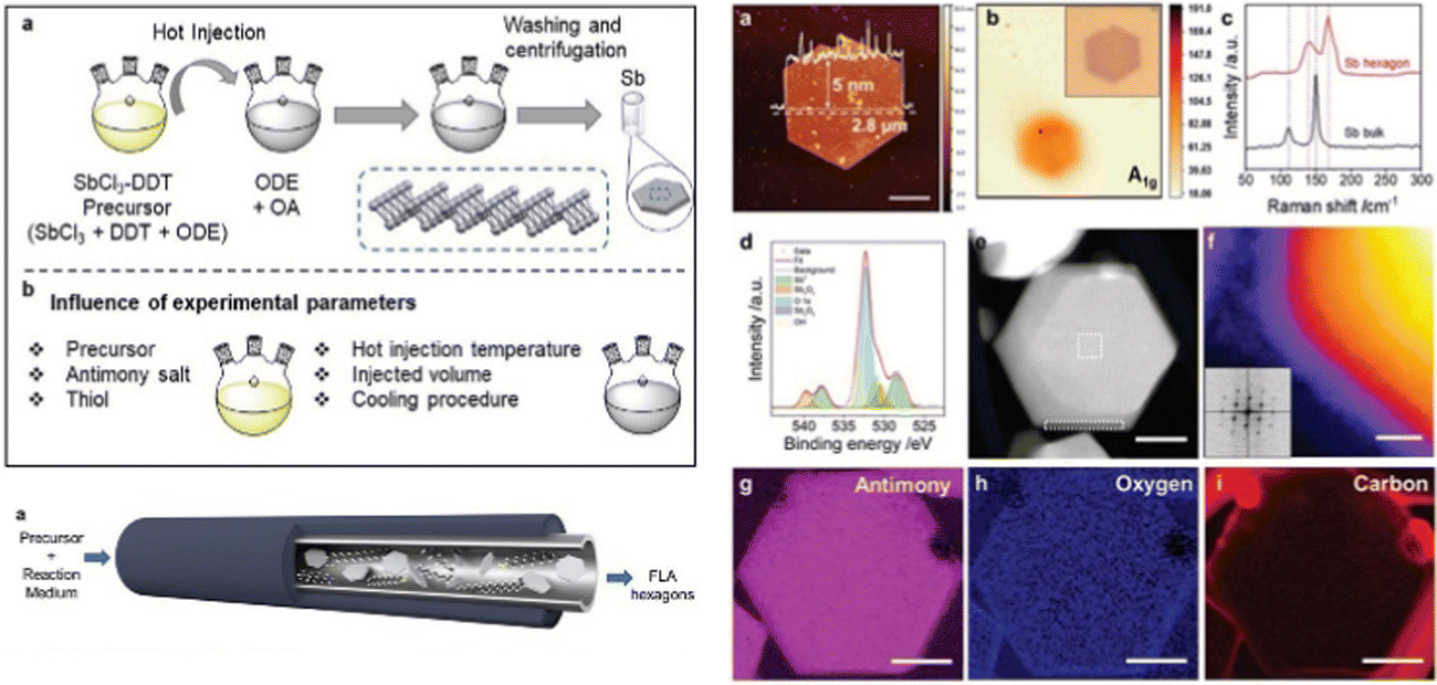 | ||
| Fig. 17 Main approaches in solution-phase synthesis of antimonene hexagons. Above: Schematic representation of hot injection method and parameters influencing the outcome of the synthesis. Below: Illustration of the continuous-flow reactor. On the right, different characterization performed in the obtained antimonene hexagons from the optimized solution-phase synthesis of antimonene: (a) AFM, (b) Raman mapping and (c) Raman spectra, (d) XPS, (e) HAADF STEM and (f) Colorized HAADF STEM, inset showing the fast Fourier transformation. (g)–(i) Elemental compositional EELS maps. Scale bar (e)–(i) 100 nm. Adapted from ref. 148 with permission from John Wiley & Sons, copyright 2021. | ||
To sum up, Fig. 18 and Table 3 expose an historical timeline and general overview of the main synthetic approaches developed for antimonene, highlighting the main aspects associated with each of them.
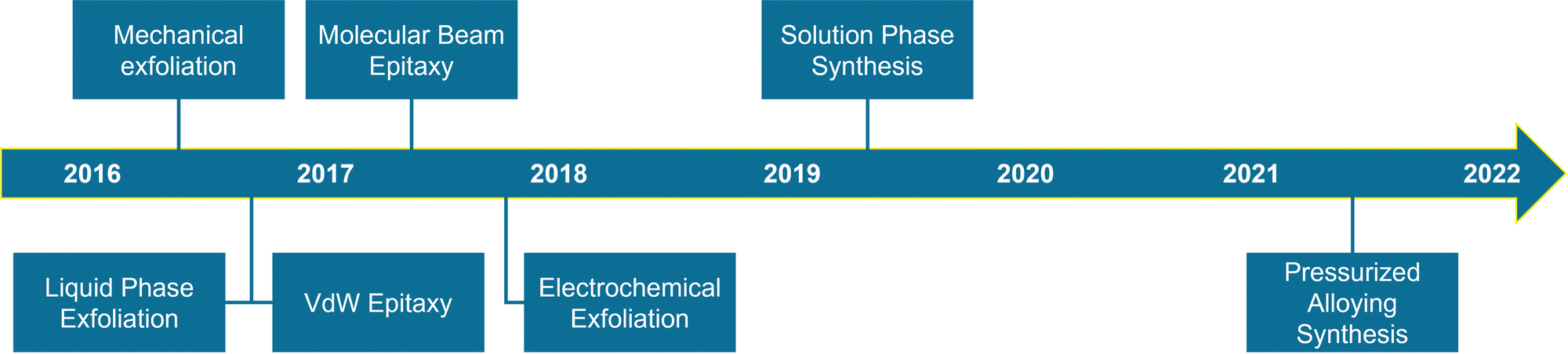 | ||
| Fig. 18 Timeline highlighting the development of the different synthetic approaches to obtain antimonene. | ||
| Synthetic approach | Main aspects | Ref. | |
|---|---|---|---|
| Top-down | Micromechanical exfoliation | • First isolation of few and single-layer antimonene | First time reported:84 |
| • Milimeter-sized crystals | Other works:149 | ||
| • Easy identification (optical microscopy) | |||
| • Low quantity of exfoliated material, time consuming, irregular morphology and lack of homogeneity in exfoliation. | |||
| Liquid phase exfoliation | • Suspensions of the material in adequate solvents (NMP, DMF, and IPA…) | First time reported:121 | |
| • Based on solubility parameters | Other works:112,124,125,150 | ||
| • Size selection (cascade centrifugation) | |||
| • Micrometer-sized crystals of few-layer antimonene (AFM) | |||
| • Irregular morphology and polydispersity. | |||
| Electrochemical exfoliation | • Two-electrode cell | First time reported:126 | |
| • Electrolyte solution containing few-layer antimonene dispersion. | Other works:107,151 | ||
| • Size selection (cascade centrifugation) | |||
| • Micrometer-sized crystals of few-layer antimonene (AFM) | |||
| • Irregular morphology and polydispersity. | |||
| Pressurized alloy assisted synthesis | • Uses pressure created from the protonation of the alloy, creating a buoyancy that exfoliates antimonene | First time reported:133 | |
| • Irregular morphology, wide size distribution, but very thin flakes (1–2 nm) | |||
| Bottom-up | Epitaxial growth | • Molecular beam epitaxy (MBE) and van der Waals epitaxy (vdWE) | First time reported: MBE,140 vdWE117 |
| • Used to grow antimonene on substrates (mica, Ge(111), Ag(111)…) | Other works:81,108,141,142,152–155 | ||
| • Micrometer-sized crystals of single-layer antimonene (AFM) | |||
| • Irregular morphology, low quantity if the material and polydispersity. | |||
| Solution-phase synthesis | • Based on the anisotropic growth of antimonene | First time reported:144 | |
| • Large-scale production of the material | Other works:145,148 | ||
| • Micrometer-sized crystals of few-layer well-defined hexagonal antimonene (AFM) | |||
| • Polydispersity |
4. Novel insights on the characterization and chemical reactivity of antimonene
Regarding the most typical characterization techniques to confirm the identity of antimonene, there are the following: microscopy techniques, X-ray diffraction (XRD), Raman spectroscopy and XPS. Firstly, microscopy measurements (HRTEM, SEM, AFM or optical microscope, among others) are fast techniques to check the layered morphology of the material. As previously commented, optical contrast is reported as a feasible way to identify the quality of the layered system.149 AFM is positioned as the best tool to study the thickness (i.e. the number of layers) of the deposited antimonene (Fig. 10). In this sense, it is mandatory to consider that the water molecules trapped between the antimonene and the substrate overestimate the measured thickness.86 Taking this into account, a monolayer of antimonene exhibits an average height of ca. 0.9 nm, while a few-layered system is obtained in high yield with thicknesses in the 4 nm range and several μm in lateral dimensions.84,121 In order to unveil if a thin flake is a monolayer, one can fold the terrace via nanomanipulation with the AFM into an origami structure. As previously reported by Geim and Novoselov concerning graphene sheets, a single flake can be identified by measuring the step height of single folds.85 As reported by Ares et al.,84 the lowest step height was found to be 0.4 nm hence corresponding to a monolayer of antimonene. This origami folding was also performed days after the flake deposition on the substrate, thus confirming the mechanical stability of the material. Furthermore, high-resolution AFM allows the ability to study the atomic periodicity, and hence it is useful to relate it with the phase of antimonene. Due to the rippling effects caused by the conformation of antimonene to the underlying SiO2, it is very difficult to obtain well-resolved atomic force microscopy (AFM) images that exhibit the atomic periodicity. This effect is also visible for graphene on SiO2, therefore not ascribed to the antimonene itself.156 Regarding AFM data, it is of utmost importance to correlate them with those of other techniques such as Raman spectroscopy to successfully identify the layered material (Fig. 10).157 In the absence of this supporting evidence, one can easily mistake solvent impurities for “fake flakes” of the desired material.Electron microscopy provides the morphology of the material and is revealed as a key technique in the search for a desired morphology, such as well-defined hexagonal samples in solution phase synthesis or the AMQDs.127,144 Even though TEM, HRTEM or SEM cannot be used to analyse the thickness of the sample, they can be used for measuring the average lateral dimension as well as taking wider areas of the deposited material throughout the whole substrate. In this context, aberration-corrected scanning transmission electron microscopy (STEM) combined with EELS can be used to investigate the local structure and chemistry of the flakes (Fig. 19–21). For example, for LPE samples, high-angle annular dark-field images taken at low voltages to prevent damaging the flakes highlight the atomic-resolution of the crystal structure, confirming a β-phase as well as the good crystallinity and the absence of defects in the studied antimonene flakes. The EEL spectra depict the compositional maps according to absorption edges such as Sb M4,5, O K or C K, pointing out some damage in the flake ends and the presence of elements such as C and O because of surface contamination and oxidation.121
 | ||
| Fig. 19 (a) Atomically resolved STM image of an antimonene monolayer on SbAg2 surface alloy on Ag(111). (b) The simulated STM in the constant height mode (∼2 Å). (c) Schematic representation of the layer-dependent A17 (AB α-2D-Sb) transition to A7 in antimonene. (d) LEED pattern of 2D-Sb on graphene. Part of the Ewald sphere at 44 eV is shown in the bottom left and at 29 eV is shown in the top right. (e) STEM of a cross section of 4 bilayers A17 antimonene island on graphene. Adapted from ref. 82 and 152 with permission from American Chemical Society, copyright 2020. | ||
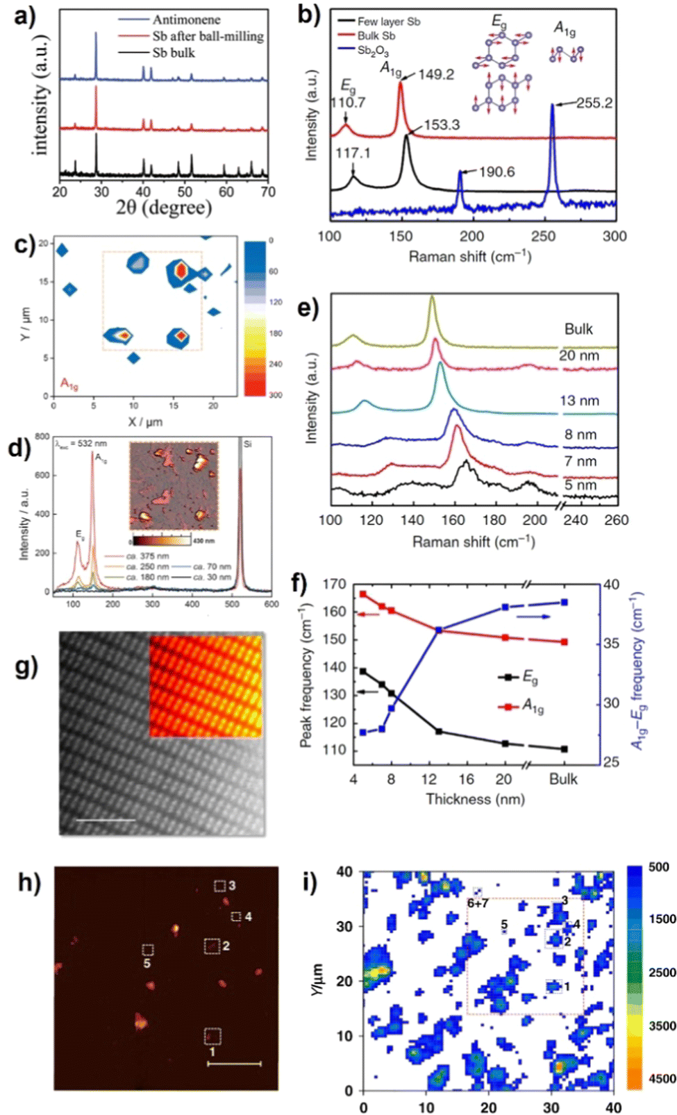 | ||
| Fig. 20 (a) X-ray diffraction (XRD) patterns of bulk antimony crystals, antimony plates after ball-milling and antimonene. (b) Raman spectra of bulk antimony (β-phase), few-layer antimonene and antimony trioxide. Inset: Vibrational modes of β-phase antimonene. (c) A1g intensity Raman mapping of solvent-exfoliated flakes deposited on a SiO2/Si substrate. (d) Single-point Raman spectra measured at different thicknesses according to the topographic AFM image (inset) of the same area studied in (c) (dashed lines). (e) Raman spectra of antimonene polygons with different thicknesses, from 5 nm to bulk. (f) A1g, Eg peak frequencies and energy difference of those two peaks plotted against sample thickness. (g) Atomic resolution HAADF image acquired on the edge of a free-standing portion of an antimonene flake obtained by LPE. The scale bar is 2nm. (h) Representative AFM topography image (scale bar 5μm) of exfoliated antimonene onto SiO2/Si substrates. (i) The corresponding Raman A1g mapping of the same antimonene flakes in (h). Adapted from ref. 65 and 117 with permission from Springer Nature, copyright 2019 and 2016, ref. 121 with permission from John Wiley & Sons, copyright 2016, and ref. 158 with permission from the Royal Society of Chemistry, copyright 2020. | ||
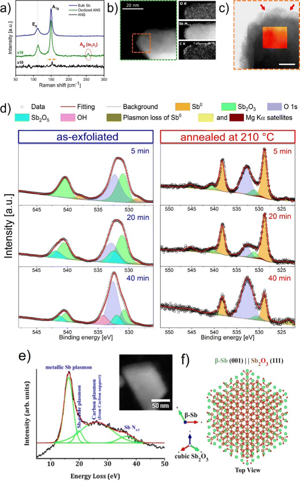 | ||
| Fig. 21 (a) Raman spectra of bulk antimony, exfoliated ANS and oxidized-ANS exhibiting Sb2O3 Raman fingerprint at 254.6 cm−1. (b) HAADF image of sub-nanometric ANS acquired at 80 kV and the corresponding elemental compositional maps derived from EELS. (c) High-magnification annular bright field (ABF) image near the edge of the nanosheet displayed in (b) (orange-dashed area) (scale bar 5 nm). (d) XPS line spectra in the Sb 3d region for antimonene nanosheet samples, as-exfoliated (left column) and after thermal annealing at 210 °C under high vacuum (right column). (e) VEELS spectrum of the β-Sb(001) crystal on suspended graphene (ADF STEM in the inset). Spectrum acquired after ∼8 months ambient air exposure of the sample. (f) Atomic model of the suggested Sb2O3(111) formed from ambient air exposure on β-Sb(001) crystals. Adapted from ref. 83 with permission from Springer Nature, copyright 2021, and ref. 125 with permission from IOP Publishing, copyright 2020. | ||
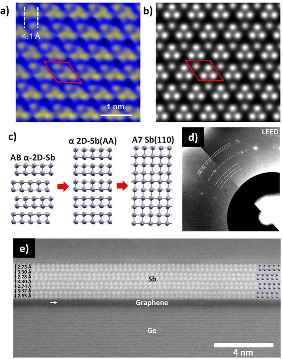
Moutanabbir et al. have recently used scanning tunneling microscopy (STM) and STEM, together with state-of-the-art techniques, like in situ low-energy electron microscopy (LEEM) or X-ray photoemision electron microscopy (XPEEM) to observe the allotropic state of antimonene grown by MBE on top of graphene Ge heterostructures. These techniques are optimized for surface observations, as the low energy of the electrons gives high sensitivity to surface signals due to their strong interaction, with resolutions greater than 10 nm in some cases. The measurements revealed a stabilized α-phase (A17) of the antimonene in flakes thinner than 4 nm (Fig. 19(e)), which undergo a thickness-driven transition to the stable β-phase (A7) as the number of layers increase (Fig. 19(c)).82 This allotropic dynamism as function of thickness is intimately related to the electronic structure of antimonene.
Further studies about antimonene/graphene heterostructures have been carried out by Bayer et al, where they studied the allotropic phases of antimonene grown by vdWE onto CVD graphene. They found the coexistence of two main morphologies: 2D rhombohedral β-antimonene, and a one-dimensional nanowire structure with rectangular basis.83 Remarkably, both morphologies exhibit direct in-plane rotational vdW epitaxy with the graphene support. These results open the door for the scalable production of antimonene heterostructures by bottom-up approaches.
As in other 2D materials prepared using top-down approaches, XRD is one of the most commonly used techniques because it can confirm the diffraction patterns of the resulting product allowing identification of the antimonene crystalline phase.112,144 In this context, bulk Sb and antimonene exhibit very similar XRD patterns. The main difference relies on the weaker intensity of the (003) and (006) peaks located at ca. 23.7° and 48.5°, respectively, of the antimonene compared with that of bulk Sb.158 This effect is indicative of the reduction of the antimony crystals along the c-axis mainly.124 The rhombohedral phase of Sb is indexed as PDF#035-0732.159Fig. 20(a) depicts XRD patterns of bulk Sb, Sb micro-crystals after ball-milling and antimonene.
Raman spectroscopy is a powerful technique widely used to characterize 2D materials.59,160 The Raman spectrum of bulk Sb when excited at 532 nm depicts two main phonon peaks: A1g and Eg modes at 149.8 and 110 cm−1, respectively, and related to the in-plane and out-of-plane vibrational modes.161 Few-layer antimonene displays a shift in both bands to a higher wavenumber region (also called blueshift). In this sense, it is reported that the correlation of AFM with SRM162 indicated that antimonene samples with a thickness below 70 nm (ca. 17 layers) barely show any Raman signal (Fig. 20(b) and (c)).121 Nevertheless, taking single-point spectra at different points of the sample does evidence how the peak intensities decrease concomitantly with the thickness of antimonene (Fig. 20(d)).121 It is worth noting that these Raman results follow the same trends independently of the synthetic approach to obtain antimonene. The work of Ji et al.117 clearly illustrates how the Raman peaks of bulk Sb evolve after obtaining its layered counterpart and also compares the fingerprint for a Sb2O3 species, which exhibits a completely different pattern (Fig. 20(b)). Indeed, Fig. 20(e) shows the Raman spectra of antimonene polygons synthesized by vdW epitaxy with thicknesses varying from 5 nm to bulk. Moreover, Fig. 19(f) shows the A1g, Eg peak frequencies (left vertical axis) and the energy difference (right vertical axis) of those two peaks plotted against sample thickness, confirming the blueshift observed in LPE samples. These sorts of blueshifts have been also reported for other 2D materials and are probably attributed to the fact that lattice constant shrinks when the number of layers decreases.163,164 Last but not least, by performing the LPE under inert conditions using bmim-BF4 ionic liquid and argon-filled gloveboxes it is possible to obtain highly crystalline Sb nanosheets (Fig. 20(g)) that exhibit observable Raman signals with perfect AFM spatial correlation under environmental conditions down to the 5 nm limit, well below the previous LPE results using IPA/H2O mixtures (Fig. 20(h) and (i)).65,117 XPS analysis is an effective technique to study the oxidation state of the Sb atom as well as the surface oxidation state. In this sense, and due to the importance of this point, a thorough discussion is carried out in the following section.
4.1 Oxidation behaviour
As previously commented, it is reported that antimonene exhibits good structural integrity as well as high thermodynamic stability, even though theoretical studies predicted a high tendency for oxidation surpassing even that of phosphorene.65 This is in good agreement with the recent experimental results in which O is always detected on the surface of the antimonene sheets.111,117,121 It is believed that the oxidation of antimonene leads to a surface oxidation layer that acts as a passivation coating, thus protecting the material from further structural decomposition.60 This oxidation layer might potentially alter the final properties of the material, and eventually affect the associated applications.165 Therefore, understanding the oxidation behaviour of antimonene from the fundamental viewpoint as well as from the experimental perspective is imperative for the future development of antimonene-based technologies. Recently, Assebban et al. published a seminal work comprehensively investigating the surface oxidation of liquid-phase exfoliated antimonene nanosheets (ANS).125 First, they observed that the Raman spectra of the exfoliated ANSs featured, besides the typical vibrational modes at A1g (149.8 cm−1) and Eg (110 cm−1), additional peaks at 190.5 and 254.6 cm−1 that were ascribed to Sb2O3 (Fig. 21).Further STEM analysis combined with EELS elemental mappings has shown the formation of an amorphous layer rich in Sb and O, exclusively at the top surface and edges, which corroborated the observed partial oxidation caused by the sonochemical processing in IPA/H2O during exfoliation. The authors decided afterwards to submit exfoliated samples to thermal annealing at 210 °C under ultra-high vacuum (UHV), while tracking the surface chemistry using X-ray photoelectron spectroscopy (Fig. 21). They discovered that the thermal annealing resulted, to some extent, in the removal of previously observed surface oxide adlayer, as indicated by the in situ XPS evidence. More interestingly, by means of ultraviolet photoelectron spectroscopy (UPS), they demonstrated a change in the surface electronic properties, which upon annealing, switches from a metallic to an otherwise semiconducting material with an estimated band gap of approximately 1 eV, assuming the Fermi level is situated in the middle of the gap.
Bayer et al. also studied the oxidation behavior in PVD grown antimonene/graphene heterostructures by Valence EELS (VEELS), allowing any trace of surface oxidation to be precisely detected. VEELS revealed low levels of oxidation after 8 months of ambient exposure (Fig. 21(e)), and together with the ADF STEM FT patterns, revealed the presence of a sixfold structure that can be associated with cubic Sb2O3(111). From these results, they suggest the formation of a thin crystalline layer of Sb2O3 on top of β-antimonene (Fig. 21(f)). These results again support the spontaneous formation of a 2D surface oxidation layer that passivates the structure of antimonene endowing the material with an outstanding environmental stability.83,166 This technique allows both spatial and chemical resolution of the surface of the flakes to be obtained with great precision. In particular, the XPS data of the flakes revealed the presence of an oxidation layer with a binding energy (BE; 530.9 eV) larger than the value expected for Sb2O3 (530 eV) and slightly higher than the value expected for Sb2O5 (530.8 eV). The O2 peak also presented a higher BE value (532.61 eV) compared to most of the metallic oxides (531–528 eV), thus pointing to a superficial oxidized component present only on the outer surface and not presenting a conventional oxidation pattern. These results collected in 2017 by Abellán et al. already pointed to the spontaneous formation of antimonene oxides and suggested an explanation for the great stability of antimonene under environmental conditions.
Along this front, an experiment that has been key to understanding this behavior has been the one developed by Lloret et al. using highly concentrated bmim-BF4 exfoliated antimonene suspensions investigated by XPS. As can be observed in Fig. 22, next to the broad O 1s signal at 533eV from the surface enriched ionic liquid contamination, the Sb 3d region between 525 and 545eV of the FL-Sbsus sample (Fig. 22 right, spectrum II) reveals very weak Sb 3d3/2,5/2 signals from Sb in oxidation state zero at 528.2eV for the 3d5/2 level, along with minor contributions from Sb in the higher oxidation state at around 530.3eV. Removing most of the excess IL by heating in ultra-high vacuum clearly showed Sb signals originating mostly from bulk antimony zero (spectrum III). Finally, exposing the heated FL-Sbsus sample without the protecting IL medium for several hours in air led to a significant decrease in Sb(0) and concomitant increase of the oxidized Sb species (spectrum IV); these findings thus demonstrate the role of bmim-BF4 in stabilizing the antimonene against oxidation, and more importantly, demonstrate the reactive nature of LPE antimonene with a pronounced oxophilicity. These findings are of uttermost importance as they first confirm the passivation of the antimonene surface by an oxide layer that shields it from further structural degradation, thus explaining the high stability of antimonene in comparison to its counterpart black phosphorus.167 Second, they demonstrated a novel modification approach to tailor its properties by opening a bandgap. In the same context, and by means of first-principles calculations, Zhang et al. presented a new class of tow-dimensional structures of antimonene oxide. These theoretical predictions are based on a monolayer antimonene with Sb![[double bond, length as m-dash]](https://www.rsc.org/images/entities/char_e001.gif) O double bonds perpendicular to the antimonene plane [type (I) structure], and depending on the oxygen content, tunable direct bandgaps ranging from 0 to 2.28 eV have been calculated.165 Later on, Wolff et al. realized that the fully oxidized antimonene monolayers presented by Zhang et al. are metastable and likely undergo a transition into a more stable configuration.168 Based on density functional theory (DFT) calculations, they proposed a novel type of 2D antimony oxide single- and few-layer structures in which the oxygen atom is incorporated into the antimonene planes and is bound to at least two antimony atoms (Sb–O–Sb) [type (II) structure] (Fig. 23). They have also found out that, depending on stoichiometry and the type of bonding, the proposed 2D layers exhibit different structural stability and electronic properties, ranging from topological insulators to semiconductors with direct and indirect band gaps between 2.0 and 4.9 eV. More interestingly, they foresaw that semimetallic few-layer antimonene can naturally form heterostructures with semiconducting oxidized layers, and they have presented the corresponding vibrational modes, which agree with the experimental findings on liquid-phase exfoliated few-layer antimonene.125
O double bonds perpendicular to the antimonene plane [type (I) structure], and depending on the oxygen content, tunable direct bandgaps ranging from 0 to 2.28 eV have been calculated.165 Later on, Wolff et al. realized that the fully oxidized antimonene monolayers presented by Zhang et al. are metastable and likely undergo a transition into a more stable configuration.168 Based on density functional theory (DFT) calculations, they proposed a novel type of 2D antimony oxide single- and few-layer structures in which the oxygen atom is incorporated into the antimonene planes and is bound to at least two antimony atoms (Sb–O–Sb) [type (II) structure] (Fig. 23). They have also found out that, depending on stoichiometry and the type of bonding, the proposed 2D layers exhibit different structural stability and electronic properties, ranging from topological insulators to semiconductors with direct and indirect band gaps between 2.0 and 4.9 eV. More interestingly, they foresaw that semimetallic few-layer antimonene can naturally form heterostructures with semiconducting oxidized layers, and they have presented the corresponding vibrational modes, which agree with the experimental findings on liquid-phase exfoliated few-layer antimonene.125
 | ||
| Fig. 22 Left: (a) Sb 3d image for the reference sample. Letters refer to the antimonene flakes studied. (b) Sb 3d peak for the reference sample, corresponding to point B in (a). Numbers identify the different components: 1 (Sb 3d5/2), 2 (oxidized Sb 3d5/2), and 3 (O 1s). Peaks at higher BEs are the Sb 3d3/2 components. (c) The Sb 3d image for the functionalized antimonene. (d) Sb 3d peak for the functionalized sample, corresponding to point E in (c). The peak identification and other details are as in (b). The size of images in (a) and (c) is 40 × 40 μm. Right: XPS Sb 3d and O 1s region of the neat bmim-BF4 IL (I) showing oxygen signals from the IL surface contamination layer, of the highly-concentrated FL-Sb suspension (II) showing small signals of non-oxidized (Sb 3d5/2 at 528.2 eV) and minor contributions from oxidized (530.3 eV) antimony next to the oxygen contamination, after removal of most of the IL by heating in UHV (III), and after submitting the sample to environmental conditions for a day, showing a drastic decrease in Sb(0). Adapted from ref. 65 with permission from Springer Nature, copyright 2019, and ref. 165 with permission from John Wiley & Sons, copyright 2017. | ||
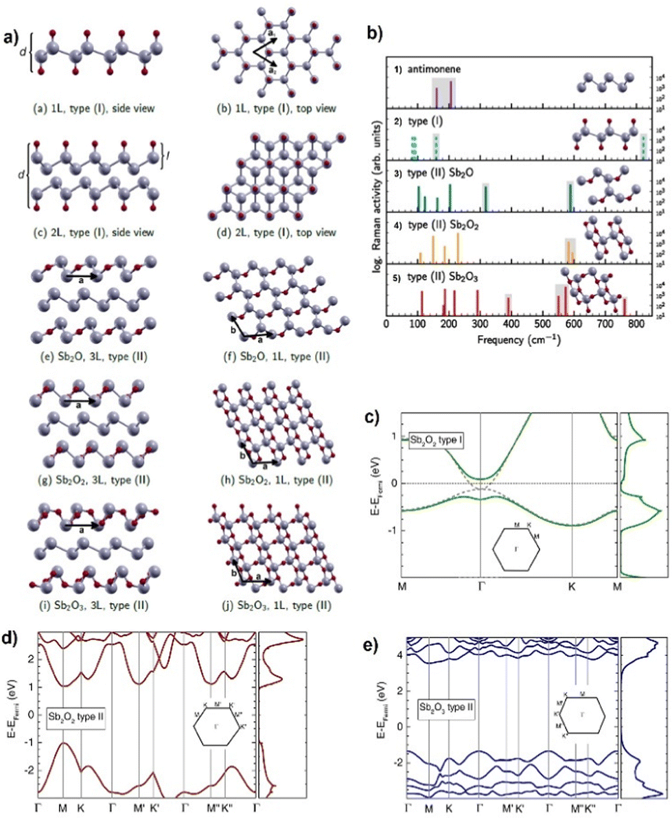 | ||
| Fig. 23 (a) Type (I) antimonene oxide structures with one layer in side view (a) and top view (b), and two layers in (c) and (d). Type (II) antimonene oxide heterostructures with different stoichiometries of the oxidized layers: (e) and (f) Sb2O; (g) and (h) Sb2O2; and (i) and (j) Sb2O3. Type (II) structures in the top view show the oxidized layer only. Oxygen (antimony) atoms are shown in red (gray). Labels a and b on the figures indicate the in-plane lattice vectors. (b) Calculated frequencies of Raman-active vibrational modes in (1) antimonene, (2) type (I), (3)–(5) type (II) antimonene oxide structures1.(c)–(e) Electronic band structures and density of states calculated using the hybrid functional HSE12 and inclusion of spin–orbit interactions (SOI) for (c) type (I) Sb2O2, (d) type (II) Sb2O2, and (e) type (II) Sb2O3 monolayers. Gray dashed lines are the results without SOI and are almost congruent with the bands with SOI for (c) and (d). The zero of energy is set to the Fermi energy. Adapted from ref. 168 with permission from American Physical Society, copyright 2022. | ||
With this knowledge in mind, it is apparent that the surface oxidation of antimonene is in most cases inevitable, especially if exposed to ambient conditions. It becomes vital, now more than ever before, to reconsider the outcomes of such drastic surface changes on the measured physical properties of antimonene, which might eventually lead to the better understanding of the current divergence in the reported experimental findings. Furthermore, it might also explain the difficulties being encountered by different research groups in conducting some of what is considered basic measurements in the realm of 2D materials, such as electrical contacts and determination of the electronic band gap.
Through this section of the present review, we aim at stimulating the scientific community to revive the discussions related to this fundamental aspect of antimonene. For instance, Gibaja et al. observed that the ultrasonication-induced oxidation of liquid-phase exfoliated antimonene comparatively enhanced the electrocatalytic performance towards the hydrogen evolution reaction (HER) under acidic pH.112 Likewise, Bat-Erdene et al. demonstrated that surface-oxidized few-layer antimonene nanosheets can be an efficient nitrogen reduction reaction (NRR) catalyst for the electrochemical synthesis of NH3.169 According to the same authors, the activation of the NN bond for the NRR process is facilitated by the oxidized species of antimonene as a result of the more favourable adsorption energy of N2 caused by the increase in polarity, as compared to non-oxidized antimonene. Furthermore, Duo et al. proved that ultrathin antimonene nanoparticles (AMNPs) are effective radiosensitizers that can achieve efficient radiochemotherapeutic effects.170 As the authors explained, X-ray irradiation induced reactive oxygen species (ROS) overproduction and accelerated the valence transition to toxic Sb2O3, eventually leading to cancer cell death. Finally, yet importantly, it turned out that the oxidation of antimonene is highly desired in many applications, as opposed to the detrimental oxidation of black phosphorus. Therefore, the development of a fast, effective, and reliable method to realize the expected antimonene oxide systems is an urgent demand. Fickert et al. have recently introduced a proof of concept of such a method, by which they realized arbitrary heterostructures of Sb2O3/antimonene through a spatially resolved laser-induced oxidation of antimonene on the sub-μm scale.98 Although a fine control of the O distribution and concentration is still to be achieved, it provides an indisputable experimental evidence of its practical feasibility. In the same context, Han et al. have successfully synthesized two-dimensional Sb2O3 crystals down to the monolayer thickness using passivator-assisted vapour deposition (PAVD) (Fig. 24).171 The crystal structure and chemical composition have been confirmed by a set of analytical techniques, namely SAED, HAADF-STEM, EDX and EELS (Fig. 24(d)–(f) and (i)–(l)). Interestingly, the authors unravelled a reversible phase transition between α- and β-phases of Sb2O3, which could be controlled either by thermal annealing or by electron-beam irradiation. This remarkable phase transformation is accompanied by changes in the electrical properties of the crystals which switches from the insulating α-phase of Sb2O3 to the semiconducting β-phase, thus demonstrating their potential applications in phase-change devices.
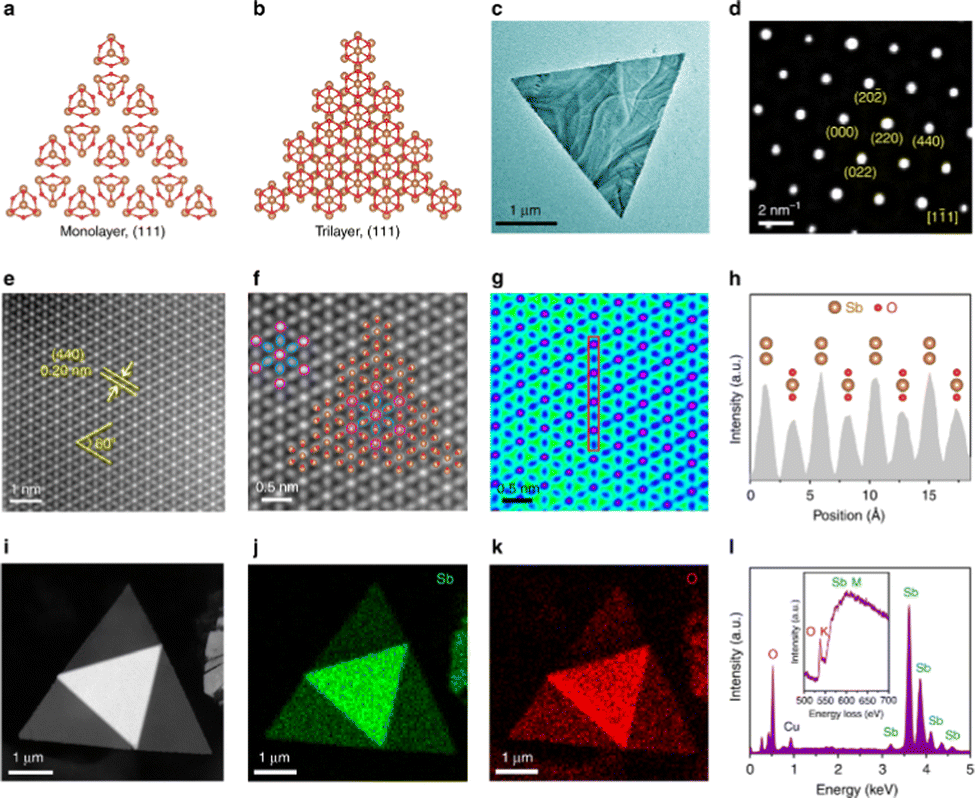 | ||
| Fig. 24 Atomic structure of 2D Sb2O3 molecular crystals. (a), (b) Top-view structural models of monolayer and trilayer Sb2O3 flakes with the (111) plane. Brown balls, Sb atoms. Red balls, O atoms. (c) TEM image of a triangular Sb2O3 flake. (d) SAED pattern of the Sb2O3 flake. (e) Z-contrast atomic-level HAADF-STEM image of the Sb2O3 flake showing the perfect atomic lattice. (f) Enlarged HAADF image and the matched atomic ball model, white atoms are marked by yellow circles and gray atoms are marked by blue circles. (g) Scattered electron intensity color image for (f). (h) Intensity line profile along the red box in (g). (i)–(k) HAADF image of a stacked flake and the corresponding elemental maps for Sb and O. (l) EDX and EELS spectra of the Sb2O3 flake. Reproduced from ref. 171 with permission from Springer Nature, copyright 2019. | ||
Last but not least, in contrast to predicted good semiconducting behaviour, experimental reports on antimonene have proved semimetal to semiconductor transitions, high carrier mobilities and strain-tunable indirect-to-direct bandgap transition, as well as the possibility of 2D and 3D topological insulator behaviour. However, due to the large allotropic/polymorphic structural diversity of antimonene, the preparation of structurally controlled ultrathin high-quality samples is very challenging. Indeed, from the physical point of view, the preparation of laterally large, defect-free monolayer antimonene films is the most important synthetic challenge. It is due to the lack of free-standing high-quality monolayer samples for device fabrication that some open questions regarding transport properties of antimonene remain unexplored. We believe that future synthetic efforts should pursue to tackle this challenge. Furthermore, once this hurdle has been overcome, the interesting topologically surface state physics of antimonene will allow its application in quantum computing or spintronic devices to be envisioned.
4.2 Chemical functionalization
Contrary to other 2D materials such as graphene or even other pnictogens like phosphorene,60,118,172 the chemical functionalization of antimonene is barely explored. Very scarce reports can be found in the literature regarding this topic.After initial predictions concerning the effect of adatoms and physisorbed molecules on the overall properties of antimonene,96,173 the first experimental evidence of a noncovalent functionalization was reported by Abellán et al. in 2017.166 In that work, the authors report the functionalization of antimonene with perylene diimide (PDI), resulting in a higher charge-transfer performance than that observed in black phosphorus (Fig. 25). The functionalization was carried out by drop-casting a THF solution of a tailormade ethylenediaminetetraacetic acid-PDI derivative on micromechanically exfoliated antimonene flakes on SiO2/Si substrates. An increase in the average thickness of the material was observed after the functionalization due to the assembly of the PDI molecules on their surfaces. Most recently, Lloret et al. also pinpointed that noncovalent functionalization with PDI leads towards the efficient passivation of BP field effect transistors (FET), paving the way for the use of PDIs to preserve the electronic properties of 2D Xenes.174
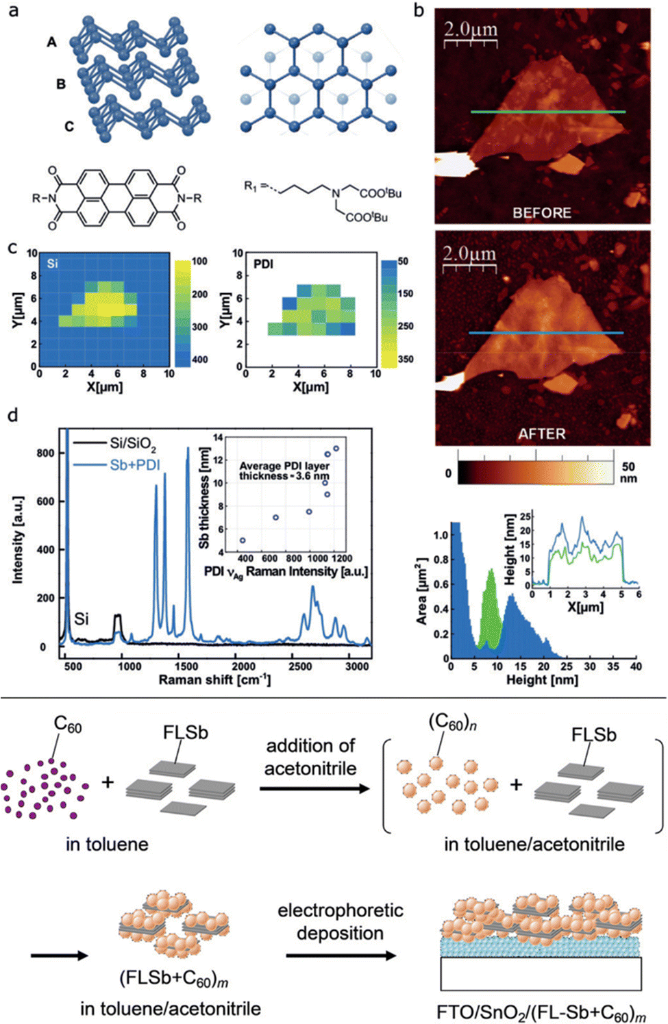 | ||
| Fig. 25 Top: (a) Structure of β-antimonene (top panel) and the perylene bisimide (PDI) molecule (bottom panel). (b) AFM topographic images showing an antimonene flake of about 10 nm of thickness. Top: Flake as deposited. Middle: Same flake after the functionalization with PDI molecules. Bottom: Height histograms of the flake before (green) and after functionalization (blue), showing an average thickness increase of 4.1 nm. The average PDI coverage in all the studied flakes was 3.6 nm. The inset shows representative profiles corresponding to the lines in the images. (c) Scanning Raman microscopy (SRM) of the same flake. Left: Silicon intensity Raman map showing a decrease in the 521 cm−1 signal which clearly reveals the morphology of the flake. Right: Raman intensity mapping shows the exclusive self-assembly of the PDI on the antimonene flakes and not on the Si/SiO2 substrate. (d) Mean Raman spectra (excitation at 532 nm) of the flake showing the PDI bands as a consequence of the quenching of its fluorescence. Bottom: Formation and electrophoretic depositions of FLSb-C60 composite clusters. Adapted from ref. 166 and 176 with permission from John Wiley & Sons, copyright 2017 and 2020. | ||
The scanning Raman microscopy of the flakes before and after PDI insertion highlights a significant quenching of fluorescence which allows the characterization of the PDI spectrum with excellent quality. The exclusive self-assembly of the PDI molecules on the top of antimonene flakes with no traces of them on the SiO2/Si substrate is worth noting. Furthermore, there is a clear correlation between the thickness of the organic coverage and the quenching of fluorescence when the former is below 4.5 nm (ca. 10 monolayers). Nevertheless, for a thicker coverage, an increase of the background coverage takes place concomitantly with the decrease in PDI Raman intensities. XPS spectra confirm the grafting of the PDI molecules pointing out a shift in the functionalized sample and thus the charge-transfer effect. This effect is ascribed to the electron-withdrawing behaviour of PDI molecules as seen in other 2D materials.175 Besides, scanning photoelectron microscopy combined with computational studies demonstrates the nature of the strong noncovalent interaction between PDI and antimonene indicating a significant charge transfer effect from the antimonene to the PDI of about twice as large as the observed for phosphorene.60 Regarding the possibility to remove the PDI adlayer with temperature, a temperature-dependent Raman analysis was carried out. The results exhibited a complete degradation of the PDI coverage at 400 °C (which starts removing at 300 °C), while antimonene flakes remain stable up to 450 °C, where degradation occurs. In addition to the study of PDI noncovalent functionalization on micromechanically-exfoliated flakes, the work also tests the functionalization of antimonene dispersions prepared by LPE.166 PDI grafting led to a fluorescence quenching of 80%, higher than that of black phosphorus (66%).60 Finally, tetracyano-quinodimethane (TCNQ) was used as an additional grafting molecule (instead of PDI) to further confirm the charge-transfer process.166
Another work related to noncovalent functionalization is the one reported by Imahori and co-workers with fullerene clusters.176 In this approach, the resulting hybrid material was synthesized after combining few-layer antimonene with fullerene clusters in a mixture of a poor solvent such as acetonitrile with a good solvent like toluene as depicted in Fig. 25. This work is focused on the photochemical properties, exhibiting a rapid rise in transient conductivity for the hybrid, while no signal is observed in the single component. The reported results open the door to the fabrication of inorganic–organic antimonene hybrids of interest in optoelectronic devices.
In addition to the noncovalent functionalization previously reported with discrete molecules, Zamora and co-workers recently reported the functionalization of few-layer antimonene with oligonucleotides for DNA sensing.177 The work highlights the supramolecular interaction between the two materials supported theoretically and experimentally. Theoretical analysis confirmed that the single-stranded oligonucleotides adopt different conformational configurations after interaction with antimonene. Because of that, one of those possible arrangements allows the nucleotide to hybridize with its complementary nucleotide, which is the basis for the development of a DNA sensor.
A completely different approach was recently reported by Su et al. showing the synthesis of halogenated antimonene nanosheets composed of oxygen and halogen-decorated amorphous and crystalline domains.151 Halogens are common species used in the surface functionalization of 2D materials because of their high electronegativity, which allows them to bond most of the metallic or non-metallic atoms. In this sense, it is also reported that halogenated 2D materials exhibit enhanced properties if compared with the pristine samples. The halogenated antimonene was synthesized concomitantly with the electrochemical exfoliation of bulk Sb as detailed in Fig. 26. To carry out the halogenation, the electrolyte was an acetonitrile solution of 1-ethyl-3-methylimidazolium (EMIM) [BF4], [EMIM][Cl], [EMIM][Br] or [EMIM][I] as the source of F, Cl, Br or I atoms, respectively. It is expected that the halogenation process takes place via the formation of halogen radicals that intercalate themselves into the interlayer region of Sb crystals, thus weakening the van der Waals interactions between layers and hence expanding the interlayer space.
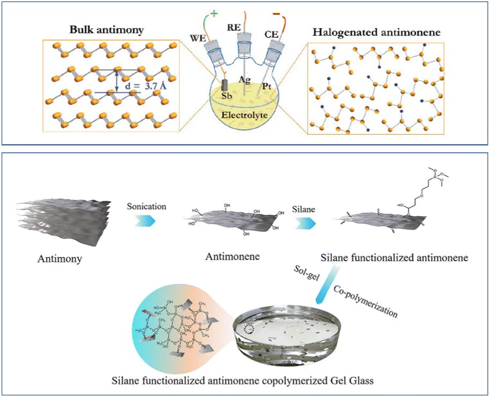 | ||
| Fig. 26 Top, schematic illustration of the experimental setup for the electrochemical exfoliation and synchronous halogenation of antimonene in an ionic liquid-based electrolyte. Bottom, schematic illustration for the preparation of silane-functionalized antimonene nanosheets and their copolymerized gel glasses. Adapted from ref. 151 with permission from John Wiley & Sons, copyright 2019 and ref. 179 with permission from American Chemical Society, copyright 2021. | ||
The XRD characterization of the halogenated sample shows no additional peaks after functionalization, discarding the presence of SbX species. Regarding Raman spectroscopy, the typical vibrational modes of antimonene are suppressed and become undetectable, in a similar way to what happens with fluorinated graphene.178 All thicknesses were estimated with AFM giving rise to average values of 2.5 nm, ascribed to a few-layer system and taking into account the surface adsorption of O and halogen atoms. Interestingly, XPS also highlights the successful preparation of halogenated antimonene. All spectra evidence Sb–Sb bonds that indicate the intrinsic metallic antimonene, as well as Sb–O and Sb–X bonds. In this context, the degree of functionalization can be semiquantitatively estimated according to the chemical bonds concentration by dividing the overall peak area of Sb–O and Sb–X signals with the Sb 3d5/2 integral area. The results gave rise to a higher degree of functionalization for Cl and I (ca. 47%) followed by F (38%) and Br (25%).151 Concerning the application as photodetectors, the photoresponse performance under UV and visible light of halogenated antimonene was investigated. All samples depicted photocurrent on/off behaviour at 0 V, increasing the photocurrent signal under a fixed external applied voltage of 0.6 V. However, the overall performance of halogenated antimonene is lower than that of the pure material.
Finally, the covalent functionalization of antimonene has been recently reported by Xing et al. using 3-glycidoxypropyl-trimethoxysilane achieving silane-functionalization.179 Silane functionalization has been explored in 2D materials such as graphene or LDHs, among others,180,181 The functionalized antimonene material was obtained as a copolymerized gel glass after the silane hydrolysis and polycondensation reaction (Fig. 26). The resulting gel glass depicted outstanding nonlinear and optical performances, with a strong ultra-broad-band optical limiting performance focused at 532–2150 nm. This optical limiting feature comes as a combination of nonlinear absorption, nonlinear refraction, and nonlinear scattering. This work paves the way for using silane-functionalized antimonene and their copolymerized hybrids in different fields such biology, energy or optoelectronics.
Rao et al. investigated the functionalization of antimonene using group 12 and 13 Lewis acids.182 They were able to obtain antimonene nanosheets with blue-shifted emission, depending on the Lewis acid used. The interaction of the lone pairs on Sb led to the formation of Lewis acid–base adducts that show a lattice distortion due to the charge transfer from Sb to the Lewis acid and steric repulsions. The functionalized antimonene nanosheets showed a red-shift in the vibrational modes which depended on the strength of the Lewis acid, being more prominent in the A1g mode, showing that the effect in the out-of-plane lattice constant is greater than the in-plane. Together with the rehybridization of the band structure, that allowed the blue-shift of the antimonene nanosheets emission, they demonstrated a functionalization procedure that allowed for tuneability and surface passivation.
Rao et al. also covalently functionalized antimonene and bismuthine nanosheets using p-nitrobenzene diazonium salts.183 The study of the reaction mechanisms demonstrated the transfer of lone pairs of electrons from the metallic Sb to the diazonium salts, forming a quaternary Sb+ species with organic moieties predominantly attached through Sb–C bonds. This functionalization led to lattice distorsion and charge transfer in the antimonene nanosheets, reducing their bandgap from 2.23 to 2.18 eV, demonstrating the tunability of the optical properties and surface passivation.
5. Applications
As previously commented in this review, the practical applications and properties of antimonene are still emerging. However, there are different works that propose a broad range of feasible applications, including proof-of-concept devices and processes that can be classified into optoelectronic devices, catalysis and electrocatalysis, energy storage, and last but not least, in biomedical applications like cancer therapy or biosensing, which we believe holdsgreat promise for the following years. Below we will detail each of them, showing their potential and future prospects.5.1 Optoelectronic devices
Optoelectronic devices require materials that are both responsive to visible light as well as able to transfer carriers. In this sense, 2D conductors benefit from appropriate bandgaps and high mobilities.15,184 From the practical point of view, Wang et al. reported the first use of antimonene with the adequate bandgap as a hole transport layer (HTL) in a perovskite solar cell (Fig. 27).185 The assembled device was built as an ITO/antimonene/perovskite/PCBM/Bphen/Al heterostructure (PCBM = [6,6]-phenyl-C61-butyric acid methyl ester). Antimonene was obtained after pregrinding bulk Sb into Sb plates that were transformed into antimonene by means of LPE assisted by sonication. The final material was obtained after successive centrifugation at different speeds while studying the bandgap dependence on the thickness, which was tuned in the 0.8 to 1.44 eV range (probably related with different degrees of surface oxidation). The energy level of antimonene closely matches that of methylammonium lead iodide (MAPbI3) perovskite, hence suggesting an adequate driving force for the hole extraction. This fact is also confirmed by the strongly quenched photoluminescence of the perovskite on top of the ITO/antimonene. This is indicative of the prevented radiative recombination due to photoinduced charge separation. The use of the material as an HTL gave rise to an enhancement of in the hole extraction and photocurrent of ca. 30%, from 11.2 to 14.6 mA cm−2 for the HTL-free (control sample) and the antimonene device, respectively. In addition, the external quantum efficiency (EQE) in the entirely visible light was enhanced from 45% to 55–60% for the control and antimonene device, respectively. Additionally, Wang et al. also reported the use of antimonene quantum dots (AMQDs) for assembling high-performance organic photovoltaics, enhancing the power conversion efficiency of the device ca. 25% higher than that compared with the reference device (Fig. 27).186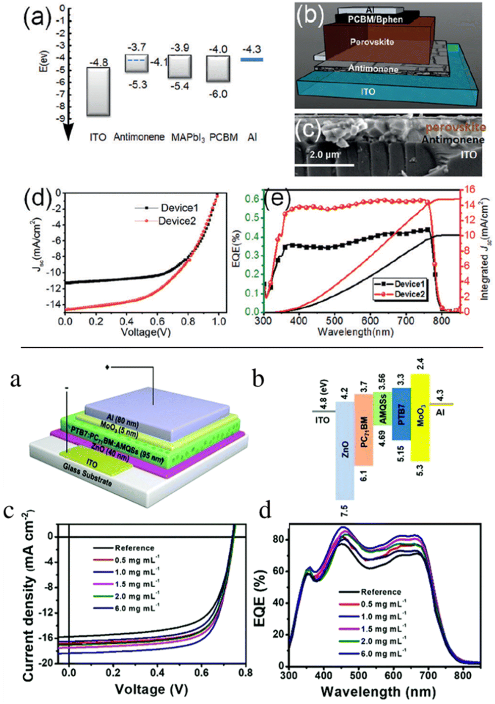 | ||
| Fig. 27 Top: (a) Comparison of energy levels of each functional layer. The Fermi level of antimonene is represented by the dashed line. (b) Configuration of the antimonene-based device. (c) Cross-sectional SEM image of the studied device. (d) Current-density–voltage (J–V) curves of devices with different architectures. (e) External quantum efficiency (EQE) spectra together with EQE-data-based integrated short-circuit current densities (Jsc) for devices 1 (HTL-free) and 2 (ITO/antimonene/perovskite/PCBM/Bphen/Al). Bottom: Device structure and performance characterization of an antimonene organic-photovoltaics device. (a) Device architecture including the AMQSs. (b) Band structure of the organic-photovoltaics device. (c) Current density–voltage (J–V) curves and (d) EQE characteristics of the best reference device and the devices with different concentrations of AMQDs in their active layer. Adapted from ref. 185 with permission from John Wiley & Sons, copyright 2018, and ref. 186 with permission from the Royal Society of Chemistry, copyright 2018. | ||
After the work of Wang et al.,185 other authors have proposed additional works on the optoelectronic applications. Lu et al. reported α-phase few-layer antimonene and AMQDs with nonlinear optical Kerr response using spatial self-phase modulation (SSPM).126 They reported a nonlinear refractive index of the few-layer antimonene of ca. 10−5 cm2 W−1, larger than that of AMQDs. Therefore, the study proposes antimonene as a new kind of promising optical Kerr material with enhanced stability, particularly at a short wavelength range. Song et al. also reported the study of the broadband nonlinear optical response of few-layer antimonene via open-aperture Z-scan laser measurement.187 Their findings confirmed the use of a few-layer antimonene decorated microfiber as an optical saturable absorber for ultrafast photonics operation and as a stable all-optical pulse thresholder that can suppress the transmission noise, boost the signal-to-noise ratio (SNR), and reshape the deteriorated input signal.187 That work was further expanded with an additional study in which they use the microfiber as an all-optical Kerr switcher with an extinction ratio up to 12 dB and a wavelength conversion of modulated high-speed signals at a frequency up to 18 GHz.188 Both reports enlighten the applicability of antimonene-based devices in high-speed optical communication. Finally, the work of Zhang et al. demonstrated that semiconducting antimonene nanosheets (probably heavily oxidized ones) exhibited indirect bandgap properties with photoluminescence bandgap of ca. 2.33 eV and a lifetime of 4.3 ns. These nanosheets were also satisfactorily tested for the hole extraction layer in planar inverted perovskite solar cells, enhancing the device performance thanks to fast hole extraction and efficient hole transfer at the perovskite/hole transport layer interface.189
Alongside optoelectronic applications, the preparation of electronic devices as field effect transistors (FETs) is also reported with antimonene. In this topic, Ji et al. reported the fabrication of thin film transistors on few-layer antimonene.117 The devices were directly prepared on mica substrates after the synthesis of β-antimonene using HfO2 as a top gate dielectric. The contacts are made of Cr and Au in the form of 10 and 30 nm thick layers, respectively. Afterwards, a 15 nm thick layer of HfO2 was grown on the top by means of atomic layer deposition, followed by a final 50 nm thick layer of Au as the top gate electrode. The electrical characterization was carried out with a semiconductor parameter analyser at room temperature, and three typical devices with antimonene thicknesses of 30, 40 and 50 nm were measured at zero gate bias. Regarding the thinnest device (30 nm), an electrical resistance of 600 Ω was measured, with an electrical conductivity of 1.6 × 10⁴ S m−1. This value is in good agreement with that expected for semimetals and consistent with the theoretical predictions. Furthermore, the antimonene devices on mica substrates exhibited high flexibility and no major changes in the conductivity were observed after bending 100 times. These results combined with the wavelength independent high transparency in the visible light range suggest antimonene as a good candidate in the elaboration of flexible transparent conducting electrodes.117
Further studies on preparing transistors are found in the works of Chang190 and Sun et al.191 The first one is focused on novel antimonene tunneling field-effect transistors (TFETs) based on the lateral monolayer (semiconducting)/multilayer (metallic)/monolayer (semiconducting) heterostructure. The proposed antimonene TFETs consist of a semiconducting monolayer of the material in combination with a small metallic multilayer region between the source and the channel. The presence of a multilayer region introduces gapless metallic states that result in the enhancement of the tunneling probability, leading to a larger current. Using the ab initio electronic structure and quantum transport calculations for different antimonene TFETs, the simulations conclude that even a 1 nm scale nanostructured multilayer can boost the current and enable abrupt device switching.190 Overall, antimonene heterostructure TFETs appear to surpass phosphorene ones because of the elimination of the tunneling barrier thanks to the locally constructed multilayer antimonene. Second, the work of Sun et al.191 is focused on the device performance of FETs composed of monolayer arsenene and antimonene in the sub-5 nm region using ab initio quantum transport simulations. They concluded that the sub-5 nm double gate monolayer assembly of arsenene and antimonene metal oxide semiconductor FETs successfully fulfills the low power requirements of the International Technology Roadmap for Semiconductors in 2028. The calculated performance outperforms that of a MoS2 analogue in terms of on-current.191
In this context, it is noteworthy to note the work of Han et al. in the synthesis of Sb2O3 inorganic molecular crystals with thickness down to monolayer previously detailed in the section focused on the oxidation behaviour.171 2D inorganic molecular crystals are still a challenge because of the difficulties in controlling both crystal phase and growth plane. The work reports the design of a passivator-assisted vapor deposition method that leads to 2D Sb2O3. The use of a passivator (InCl3 or Se), prevents the heterophase growth and promotes the lateral growth in the high-energy crystal planes. The as-synthesized α-phase of Sb2O3 depicts a thermal-induced phase transition to a mixed-phase highlighting a thermal hysteresis loop. The mixed-phase is stable from 673 to 353 K. Additionally, the insulating α-phase Sb2O3 can evolve to a semiconducting β-phase under heat and electron-beam irradiation. This fact opens the door for new opportunities in potential molecular electronic devices based on Sb.
5.2 Electrocatalysis
One of the most appealing uses of 2D materials such as MoS2 and WSe, as well as those from the pnictogen group, is their application as electrocatalysts for the electrochemical CO2 reduction reaction (CO2RR).192,193 In this context, Li et al. reported the production of few-layer antimonene nanosheets by cathodic exfoliation and tested them as a 2D electrocatalyst for the reduction of CO2 to formate with high efficiency.194 The cathodic exfoliation methodology has proven to be a simple, economic, efficient and environmentally friendly method for the large-scale synthesis of 2D materials.195,196 If compared with the bulk Sb electrode, the few-layer antimonene nanosheets electrode exhibited a lower onset potential and an enhanced catalytic current density. Furthermore, the electrode made with antimonene depicted a broad peak at ca. −1.06 V in the CO2 saturated solution which is indicative of the CO2 reduction process. The selectivity regarding H2 and formate was dependent on the applied potential, pointing to a faradaic efficiency for the formate with a maximum at around 84% at −1.06 V. On the other hand, for the CO the faradaic efficiency was found to be almost constant independent of the applied potential. In addition, the smaller antimonene nanosheets gave rise to a polarization curve Imass 3.6 times that corresponding to the larger flakes, confirming that the enhancement in the electrocatalytic activity is related to the exposed edge sites after the exfoliation. Finally, the work of Li et al. also analysed an antimonene nanosheet–graphene composite, prepared by replacing the Pt anode with a graphite rod during the exfoliation procedure. The composite depicted a higher Imass and selectivity towards formate at lower overpotentials, with a partial current density for formate 1.5 times higher than the pristine antimonene nanosheets. The enhanced activity of the composite is ascribed with both the exposure of large numbers of active sites as well as the strong electronic interaction between antimonene and graphene.197Most recently, Gibaja et al. reported the electrocatalytic properties of LPE-antimonene suspended in BuOH or NMP towards the hydrogen evolution reaction (HER).112 In this study, two parameters were chosen to compare the electrochemical performance: the Tafel slope and the overpotential required at a current density of 10 mA cm−2 (Fig. 28). The antimonene prepared in NMP showed a lower Tafel slope (145 mV dec−1) than the antimonene prepared in BuOH, while the latter depicted a lower overpotential value (–0.7 V). The reduction in the onset potential could be ascribed to both the dimensions of the nanosheets and the oxidation degree. Cyclic voltammetry curves before and after the linear sweep voltammetry showed a more pronounced redox activity for the sample in BuOH. These results are indicative of a higher degree of exfoliation of the sample in BuOH than that prepared in NMP. The cyclic voltammetry curves also highlight the irreversible oxidation processes which indicate the oxidation of antimonene into novel surface Sb oxides with specific structural and physical properties. Overall, the higher HER performance of the BuOH sample can be explained based on its better exfoliation degree and anisotropic ratio, which yield a large number of edges and therefore electroactive sites. This HER performance is also linked to the irreversible formation of Sb oxides, an effect which is more pronounced in the BuOH sample than in the NMP one.112
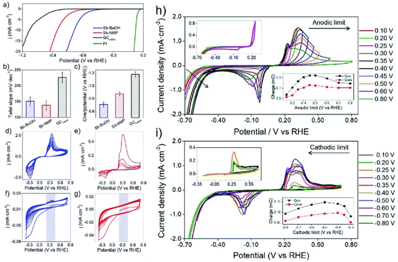 | ||
| Fig. 28 (a) LSV curves of the different FL antimonene samples, Nafion modified glassy carbon blank and platinum blank. (b) Tafel slope values and (c) overpotentials required for 10 mA cm−2 calculated from LSV data. CV curves recorded after LSV measurements of (d) Sb-BuOH and (e) Sb-NMP. CV curves recorded before LSV measurements of the (f) Sb-BuOH and (g) Sb-NMP samples. (h) Voltammograms obtained between −0.9 V and different anodic potential limits measured using 50 mV s−1. (i) Voltammograms obtained between 0.5 V and different cathodic potential limits measured using 50 mV s−1. The insets show the calculated charges obtained when a positive current is passed (Qox) or negative current is passed (Qred). Adapted from ref. 112 with permission from Royal Society of Chemistry, copyright 2018. | ||
5.3 Organic catalysis
Lewis acid catalysis is a chemical process that is mainly based on the ability of protons and/or cationic metal atoms to attract electron density from atoms of external molecules and activate them towards the attack of a third chemical entity. However, the use of non-metal species, beyond protons, is much scarcer, in particular of heteroatoms in the low-valence state. Pnictogens in the zero oxidation state (P, As, Sb, Bi) are rarely used in catalysis because of the difficulties in preparing stable materials from these elements. Nonetheless, Lloret et al. recently reported the first organic catalysis for antimonene and phosphorene taking advantage of the high degree of exfoliation and the protection against oxidation given by the ionic liquid used in the LPE process. The work focuses on the use of few-layered pnictogens as efficient catalysts for the alkylation of nucleophiles (alcohols, thiols and indoles) with alkyl carbonyl compounds (esters) in good yields and excellent selectivity (Fig. 29).65 Regarding the reaction mechanism, it is observed that the pnictogen selectively adsorbs both the nucleophile and ester on the surface thanks to the electronic stabilization of the few layers underneath promoting the coupling after formation and stabilization of alkyl carbocations on the lone electron pair network of P and Sb. Additionally, competitive tests between benzyl and decyl alcohols point to a one order of magnitude higher formation rate for the aromatic compound than for the alkyl one.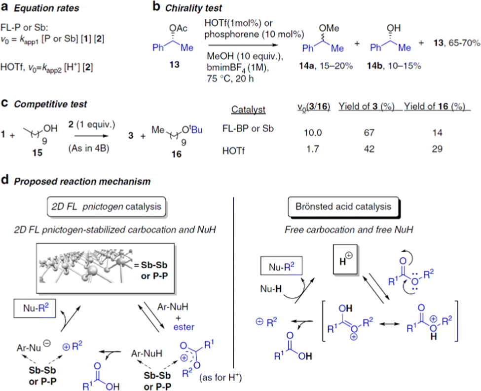 | ||
| Fig. 29 Mechanistic studies. Experimental evidence and proposed mechanisms for few-layer black phosphorus (FL-Bp), FL-Sb, and superacid triflic acid (HOTf) catalyzed alkylation of nucleophiles with esters in bmim-BF4. Reproduced from ref. 65 with permission from Springer Nature, copyright 2019. | ||
The higher polarizability of the antimonene results in a better performance than that found for the phosphorene. This mechanism enables Lewis acid catalysed processes under much milder conditions than with protons or metal cations, giving access to the alkylation of soft nucleophiles incompatible with the standard acid catalyzed conditions. This result is also in good agreement with the ability of antimonene to transfer electron charge to planar aromatic molecules, as shown in the noncovalent functionalization studies previously analyzed.166
5.4 Energy storage
The use of antimonene in energy storage is focused on its application as an anode in Na storage thanks to its high theoretical capacity of 660 mA h g−1 for Na storage as well as a low discharge potential of ca. 0.5 V (versus Na+/Na).198 It is worth noting that Na-ion batteries (SIBs) have attracted increasing attention because of sodium abundance, affordability, ease and greenness of extraction procedure.199 Nonetheless, the larger size of Na+ compared to Li+, the slow insertion and extraction of ions, and large volume changes represent the main drawbacks for developing sodium-ion batteries (NaIBs). In this sense, 2D materials in general, and 2D-pnictogens in particular, are considered one of the best alternatives for electrode materials.In fact, Gu et al. reported the synthesis of composite films made of antimonene nanosheets and graphene.124 The synthesis of Sb nanosheets was carried out via LPE starting from Sb powder in an IPA solution with constant concentration of NaOH. The resulting composite films were prepared with tunable densities, and it was observed that the volume change of metallic Sb can be successfully alleviated with the aid of the flexible graphene. As a consequence, the whole density of electrode films can be improved by harnessing the density of the antimonene nanosheets. The optimized composite film depicted a volumetric capacity of 1226 mA h cm−3 in the first cycling. This result is higher than those reported for graphene films (80 mA h cm−3) and Sb/C nanocomposites (100–300 mA h cm−3).124 In addition to that, the composite exhibited high rate capabilities for Na storage at the highest applied current of 4.0 mA cm−2, whose charge and discharge volumetric capacities were found to be initially 216 mA h cm−3 and 110 mA h·cm−3 after 100 cycles.124
Afterwards, Tian et al. discovered that the storage of Na in few-layer antimonene takes place through a sodiation/desodiation mechanism with a fast insertion of Na+ cations and a posterior in-plane alloying reaction. This effect is produced thanks to the few-layer antimonene's small diffusion barrier of 0.14 V.74 By in situ synchrotron XRD results they confirmed the reversible phase evolution of the antimonene (Sb ⇌ NaSb ⇌ Na3Sb).200 One can clearly observe how the (003) and (110) planes of the few-layer antimonene peaks were shifted to smaller and larger angles during the sodiation and desodiation process, respectively. Besides, the authors reported an experimentally measured capacity value of 620 mA h g−1, so close to the theoretically predicted value of 660 mA h g−1, thus concluding that ca. 94% of Sb atoms participate in the process for nearly 150 cycles. The schematic illustration of the proposed discharge–charge mechanism for the Sb–C NIB is depicted in Fig. 30.
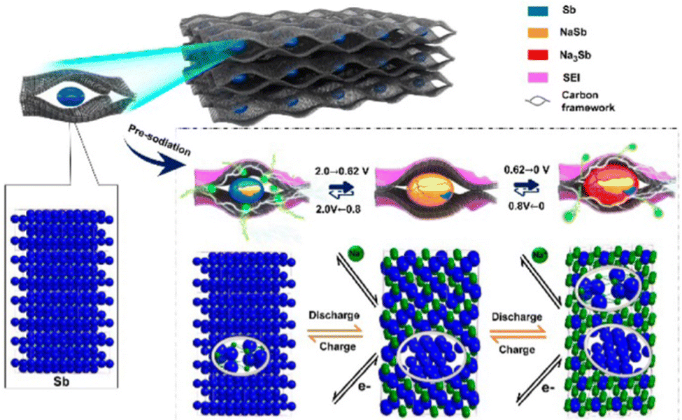 | ||
| Fig. 30 Schematic illustration of the proposed discharge–charge mechanism for the Sb–C framework film anodes as the high-performance sodium battery with unusual reversible crystalline-phase transformation. Reproduced from ref. 200 with permission from American Chemical Society, copyright 2016. | ||
Finally, Zamora and co-workers have recently reported the use of antimonene in modified screen-printed electrodes (SPE) for supercapacitors.201 They reported a significant improvement in the energy storage capabilities of a carbon electrode in both galvanostatic charging and cyclic voltammetry using 0.5 M H2SO4 as the electrolyte. Antimonene depicted an excellent performance with a specific capacitance of 1578 F g−1 measured at a current density of 14 A g−1, hence being considered as a highly promising material for energy storage applications. In line with that, the system also exhibited a highly competitive energy and power densities of 20 mW h kg−1 and 4.8 kW kg−1, respectively, in combination with good cycling capabilities. It is worth mentioning that the optimum capacitive performance has been achieved for quantities of 3.6 ng of antimonene/SPE.
5.5 Biomedical applications
In this context, the outstanding thermophysical properties and chemical reactivity of antimonene make this material an excellent candidate for photothermal cancer therapy.98
In this sense, Tao et al. reported the synthesis of novel PTAs using AMQDs coated with PEG via LPE.127 The surface modification of AMQDs with PEG enhanced the biocompatibility and stability in the physiological medium (Fig. 31). The authors reported a clear dependence of the photothermal effect with the concentration, showing a PTCE of 45.5%, higher than that observed for other PTAs such as graphene, MoS2 or black phosphorus.203 By measuring the in vitro cytotoxicity of the PEG-coated AMQDs all samples exhibited good biocompatibility. Nevertheless, it was observed that the cellular viability decreased when the AMQD concentration increased under near-infrared (NIR) radiation. This decrease was reported to be down to 10% of viable cells at a 200 μg mL−1 concentration. Fig. 31 depicts a clear separation between the living and dead cells, coloured in green and red, respectively, thus confirming the killing of cancer cells using AMQDs as a PTA combined with NIR radiation. Additionally, in vivo studies were carried out in mice with MCF-7 tumours, confirming the successful treatment of NIR irradiation combined with intratumour injection of PEG-coated AMQDs, resulting in negligible or no regrowth of the tumour. In this line, Niu et al. also focused on the PTCEs of AMQDs presenting the first excited-state dynamics study of the PTT of antimonene. Interestingly, this work highlights that the enhanced PTT of AMQDs comes from their spontaneous partial oxidation. This feature induces additional band edge states that broaden the optical absorption range and strengthen the transition dipole moment. Henceforth, this study proposes the use of oxidative AMQDs in the biomedical field.204
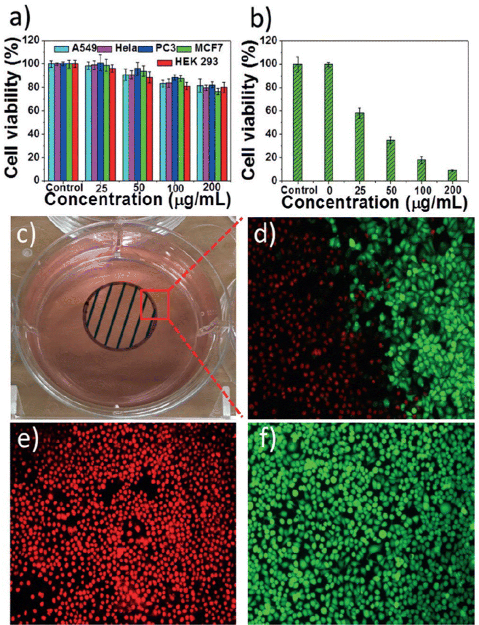 | ||
| Fig. 31 (a) Cell viability after incubation with only PEG-coated AMQDs. (b) Cell viability of MCF-7 cells treated with PEG-coated AMQDs with NIR (808 nm, 1 W cm−2) for 5 minutes. (c) A photo of the cell culture dish after incubation with PEG-coated AMQDs. The black circle with shadow shows the laser spot. (d)–(f) Confocal images of calcein antimonene (green, live cells) and propidium iodide (PI) (red, dead cells) co-stained MCF-7 cells after exposure to NIR irradiation (808 nm, 1 W cm−2). The amplification of confocal images is 100×. Reproduced from ref. 127 with permission from John Wiley & Sons, copyright 2017. | ||
Most recently, the same authors reported a photonic drug-delivery platform based on 2D PEGylated antimonene nanosheets.205 The main advantages of this platform are its excellent photothermal properties, high drug-loading capacity, spatiotemporally controlled drug release activated by NIR light and moderate acidic pH, deep tumour penetration by both extrinsic and intrinsic stimuli, excellent multimodal-imaging properties or substantial inhibition of tumour growth with no apparent side effects and potential degradability, to name a few. Furthermore, the intracellular fate of the antimonene nanosheets was revealed for the first time, leading to a better understanding of the nano-bio interactions of this class of 2D materials. The work of Tao et al. represents the first study on antimonene-based photonic drug-delivery platforms, hence paving the way for the application of this pnictogen into cancer theranostics (Fig. 32).205
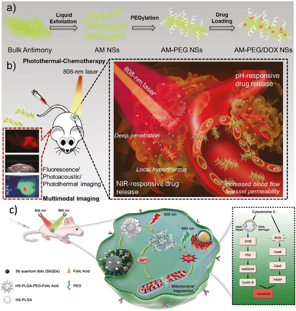 | ||
| Fig. 32 Schematic illustration of (a) the preparation of 2D antimonene-PEG-doxorubicin nanosheets and (b) their administration as photonic nanomedicines for cancer theranostics, (c) Nanopoxia treatment and methods of action. Adapted from ref. 205 and 206 with permission from John Wiley & Sons, copyright 2018 and 2020. | ||
Additionally, Lu et al. also reported the successful use of antimonene for high-performance cancer theranostics.206 In this case, the authors propose the use of cell membrane camouflage alongside dimension optimization and size control to improve the stability of antimonene. The need for enhancing the stability of this material is crucial since its use as a photothermal therapy agent is limited by its rapid degradation in physiological medium. Therefore, the antimonene sheets cloaked with the cell membrane exhibited improved stability as well as increased photothermal efficacy and superior tumour targeting capacity. Furthermore, no notable side effects were observed after using the coated antimonene as a potent photodynamic/photothermal therapy agent as an anticancer treatment during in vivo studies. In conclusion, this strategy reveals as a safe and high-performance modality of cancer therapy.207
One of the current challenges that photothermal therapy faces is the activation of inherent defence mechanisms of tumorous cells due to the overexpression of heat shock proteins in response to the hyperthermia-based treatments. To prevent this thermoresistance, Wu et al. constructed a nanocatalyst consisting of calcium carbonate, glucose oxidase and AMQDs.208 When the nanocatalyst encounters the acidic tumour microenvironment, it rapidly degrades releasing the integrated glucose oxidase and the AMQDs. The enzymatic activity of glucose oxidase effectively depletes the cellular glucose levels, reducing energy supplies of the tumorous cells and down-regulating the expression of the heat shock proteins, increasing the therapeutic performance of the photonic hyperthermia treatment. This study reveals the potential of multimodal synergistic therapies for improved biomedical effects.
Interestingly, Qiu et al. recently presented a proof-of-concept of an hypoxia-based precision cancer therapy, which they called nanopoxia.209 Taking advantage of the hypoxia conditions usually found in tumours, they developed a nanoplatform based on AMQDs encapsulated by a thermosensible polymer. Upon 808 nm laser irradiation, the SbQDs@HS-PLGA-PEG-FA outer shell is degraded, releasing the antimonene nanoparticles. In the hypoxic environment of tumours, Sb is converted into the highly cytotoxic trivalent form Sb(III), while under the normoxia conditions of healthy tissues it is completely oxidized into the less toxic pentavalent form Sb(V), achieving tumour-specific targeting and delivery of Sb. Furthermore, the oxidation of Sb can be regulated and controlled using photothermia,98,204,209 allowing a multimodal approach by combining tumour-selective toxicity of Sb, ROS production and hyperthermia treatment.
Interestingly, semimetallic mesoporous Sb-based nanospheres have been reported recently by Chen et al.207 By controlling the amount of oxygen in the synthesis of the Sb nanospheres, they selectively etched the nanospheres to obtain mesoporous materials with tuneable pore size, presenting upstanding theragnostic properties as high PTCE (44%), high photoacoustic signal, accelerated photodegradability and high drug loading efficiency.
Finally, Song et al. investigated an effective strategy to synthetize Sb nanocrystals in ligand-guided growth strategy, observing a modulation effect on the localized surface plasmon resonance depending on the morphology on the obtained antimony nanopolyhedra.210 This allowed them to increase the PTCE up to 62% when the excitation wavelength is well matched with the resonance frequency of the particles. This finding demonstrates the importance of morphology-controllable synthesis methods, allowing the fine tuning of the properties of the Sb-nanomaterials for maximizing their therapeutic potential. These results may serve as inspiration for future developments in antimonene chemistry.
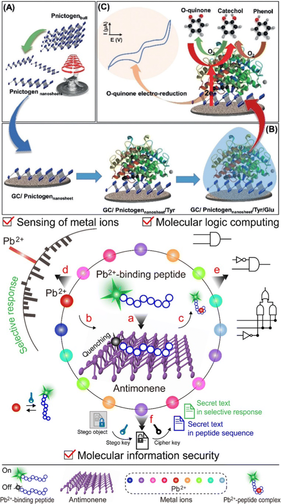 | ||
| Fig. 33 Top (a) Shear exfoliated pnictogens using a kitchen blender. (b) Biosensor preparation using layer-by-layer drop-cast pnictogen nanosheets, tyrosinase (Tyr), and glutaraldehyde (Glu) onto a glassy carbon (GC) electrode. (c) Chemical mechanism of phenol detection by a biosensor based on exfoliated pnictogen and Tyr. Bottom, scheme of a peptide fluorescence sensing system using antimonene and its different applications in the detection of Pb2+, molecular logic operations and crypto-steganography. Adapted from ref. 212 with permission from John Wiley & Sons, copyright 2019, and ref. 217 with permission from American Chemical Society, copyright 2022. | ||
Another study in the field of sensing can be found in the work of Xue et al.214 reporting a surface plasmon resonance sensor which is based on 2D antimonene, with the aim of the label-free detection of clinically relevant bio-markers such as miRNA-21 and miRNA-155. By means of first-principles energetic calculations it is estimated that antimonene exhibits stronger interaction with single-stranded DNA than graphene because of the more delocalized 5s/5p orbitals in antimonene. With an enhanced LOD up to 10.000 times compared to existing miRNA sensors, antimonene reveals as a promising material in the development of these biosensors.214
Taking advantage of this surface plasmon resonance, Singh et al. developed a nanolayered biosensing device for the detection of hemoglobin concentrations, by combining BaTiO3 and antimonene.215 In this device the antimonene is used as the bio-recognition element, due to the large surface area, its hydrophilic nature and higher absorption energy. This study further confirms the usefulness of antimonene in the sensing field, especially for biomedical applications.
Recently, Najam-ul-Haq and co-workers have developed a cost-effective biosensor based on catalase immobilized in AMQDs with the aim of determining H2O2. The key aspect in determining H2O2 is its role as a predictive biomarker of different types of cancers. The resulting material is used for the electrochemical sensing of H2O2 and tested in ovarian cancer serum pointing to a great stability and a quantitative determination of the analyte.216
As a final point, antimonene has also been proposed as a platform for peptide-based sensing. In the study by Bu et al.,217 antimonene has been used as a universal quencher of fluorescence for peptides used to sense the presence of metal ions by fluorescence. The authors claim that this platform can be used for molecular logic computing and as a nanosystem for cryptography (Fig. 33). This report provides a basic paradigm for the use of antimonene in molecular sensing platforms, opening the door to novel applications.
As previously discussed, antimonene shows a great potential in the biomedical field, with the first studies reporting the use of this material as PTA showing its great PTCE, together with an excellent biocompatibility of the PEG coated antimonene, both in vitro and in vitro.127,205,206 In terms of toxicity, the coated antimonene platforms have been tested in different cell lines, revealing a good biocompatibility, which shows enhanced toxicity after NIR radiation exposure due to the partial oxidation of the material.204 Furthermore, the first investigations of the internalization mechanisms and intracellular fate of PEGylated antimonene nanosheets demonstrated that they enter the cell primarily through micropinocytosis and caveolin-dependent pathways, and follow the classic endocytic pathway through early and late endosomes to end up in lysosomes.205 Nevertheless, most of the studies reported so far use functionalized antimonene, being coated with PEG or camouflaged using tumorous cell membranes.127,204–206 Even though these studies revealed the biomedical potential of antimonene, the use of only functionalized antimonene hinders the understanding of the effects and behaviour of the material in cellular environments, which is of critical importance for the safe and efficient use of nanomaterials.
Getting the picture of what happens with antimonene when it interacts with the biological environments (cell culture media and/or blood plasma) up to the subcellular fate of the material, addressing the alterations that it may suffer, is not an easy task. From the moment that antimonene enters in contact with the cell culture media, protein–nanoparticle interactions form the protein corona, which might affect the antimonene chemical stability and undoubtedly affects the cellular response towards the nanomaterial.220,221 The surface modification plays a crucial role in its uptake and internalization, as it is intimately related to the size, shape and surface chemistry of the nanoparticles, affecting the relative contribution of the uptake route.218,219 This in turn affects the intracellular fate of antimonene, as each internalization mechanism has different trafficking pathways, ending in diverse subcellular compartments. It is important to keep in mind that cellular organelles and compartments have utterly different chemical environments, from neutral pH compartments like endosomes or caveosomes, high molecular density organelles as the nucleus, or even very acidic and very enzymatic active lysosomes, which could affect the chemical evolution of the nanomaterial, probably modifying the nanomaterial toxicity and response. The reliable assessment of the nanomaterial and cellular association appears as a key factor in understanding the role of novel nanomaterials as biomedical tools. Nevertheless, there is no single analytical methodology capable of providing all the required information, compelling a multimodal approach, a promising strategy that offers analytical and statistical evidence to be able to obtain the full picture of these complex processes.223
6. Conclusions and outlook
This review summarizes the most important aspects of antimonene highlighting why it is considered as one of the most promising 2D materials for energy storage, high-performance opto-electronic devices, DNA sensors, cancer therapy or novel vdW heterostructures, to name a few. From its properties to its applications, this work thoroughly reviews the current knowledge on antimonene and provides an in-depth description of the material with the purpose of stimulating future research. In this sense, despite the tremendous efforts carried out during the last few years, a complete fundamental understanding of the structure–property relationships is still missing. Indeed, in contrast to graphene and other post-graphene 2D materials, experimental reports on antimonene have proved semimetal to semiconductor transitions, high carrier mobilities and strain-tunable indirect-to-direct bandgap transition, as well as the possibility of 2D and 3D topological insulator behaviour. However, due to the large allotropic/polymorphic structural diversity of antimonene, the preparation of structurally controlled ultrathin high-quality samples is very challenging. Indeed, from the physical point of view, the preparation of laterally large, defect-free monolayer antimonene samples is one of the most important synthetic challenges. This is due to the lack of this type of samples, that some open questions regarding electronic (and spintronic) properties of antimonene remain unexplored. We believe that future synthetic efforts should pursue to tackle this challenge. In any case, scientists can take advantage of the unprecedented rich allotropy of antimonene that can be engineered to some extent by playing with the synthetic strategy, substrates, morphology or thicknesses. In addition, it presents a series of phase transition mechanisms that imply great changes at the electronic level, and therefore in its interfacial properties. This dynamic behaviour holds great promise in the development of new heterostructures, both vdW and covalent, in which one can envision a novel epitaxy landscape of interest for twistronics. Another aspect that clearly differentiates antimonene from its peers (and specially from graphene) is its high chemical reactivity, leading to complex oxidation behaviour, which underlies the origin of antimonene's high environmental stability. This mouldable behaviour of antimonene that can be chemically engineered from the ground up distinguishes it from other 2D materials where little control can be exercised over the structure and properties.To this end, we can foresee that the development of antimonene chemistry will allow in a short time to obtain a controlled functionalization and a fine adjustment of the properties of the material. This will enable the development of covalent and non-covalent heterostructures, hybrid materials, and functional devices that will expand the applications of antimonene to new and exciting horizons.
In terms of applications, the use of different forms of antimonene in optoelectronic devices holds great promise in field effect transistors, perovskite solar cells or non-linear optics. It is worth mentioning that in some cases the oxidized SbxOy/Sb heterostructures outperform pristine antimonene, emphasizing the importance of controlling the synthesis of the materials. Particularly, this aspect represents one of the main differences with lighter 2D-pnictogens as phosphorene, in which surface oxidation leads to a complete degradation of the flakes. The surface reactivity of antimonene has turned out to be key for the development of catalysts, both for boosting organic reactions or electrochemical processes. In fact, while in organic catalysis it is important to preserve the antimonene surface intact in the zero oxidation state, in the electrocatalytic processes such as the hydrogen evolution reaction (HER) or the electrochemical CO2 reduction reaction, surface oxidation plays a fundamental role. We believe that through a deep understanding of the reaction mechanisms, the support of theoretical calculations and the development of new hybrid materials, current limitations exhibited by these systems will be overcome. For energy storage applications, both supercapacitors and sodium ion batteries (NIBs) have been the applications that have received the most attention. For example, in the case of NIBs, it is necessary to improve the integration of antimonene with other nanocarbon materials such as graphene to improve the cyclability of batteries by minimizing the pulverization as a consequence of charge and discharge cycles, as well as the irreversible formation of intermetallic phases. One of the greatest challenges faced by this field of research is the development of synthetic methodologies that allow obtaining antimonene of high crystalline and morphological quality on a large-scale. Along this front, novel colloidal approaches are shown as a promising alternative for applications in electronics and beyond, complementing the most established vdW epitaxy processes.
Last but not least, access to monodisperse systems such as AMQDs or colloidal routes open the door to one of the most suggestive fields of application of antimonene: biomedicine. In this direction, to the best of our knowledge, there is a lack of systematic studies aiming to rationalize the chemical identity of bare antimonene (synthetic method, size, morphology and surface chemistry) on the biomedical performance of the material, hampering the comprehension of the mechanisms governing the cellular response towards antimonene and vice versa. It will be paramount to understand the mechanism controlling the uptake of antimonene nanomaterials and how they are influenced by its physicochemical properties, as well as depicting the toxic mechanism of antimonene, relating them to the chemical evolution that it may suffer during the interaction (e.g. oxidation). A methodical study of how the properties of antimonene affect its biological performance will allow a rational design of novel antimonene biomedical platforms, with control over their stability, toxicity and biodistribution, enabling more precise biomedical nanodevices based on this novel nanomaterial. Overall, we hope that this review article will inspire novel research regarding antimonene paving the way for the development of new exciting applications.
Conflicts of interest
There are no conflicts to declare.Acknowledgements
This work has been supported by the European Union (ERC-2018-StG 804110-2D-PnictoChem to G. A.), the Spanish MICINN (PID2019-111742GA-I00, PDC2022-133997-I00, TED2021-131347B-I00 and Excellence Unit María de Maeztu CEX2019-000919-M), the Generalitat Valenciana (CIDEGENT/2018/001), and the Universitat de València and HUP/IIS La Fe (VLC-BIOMED AP2022-27). P. C-E. acknowledges the Spanish MICINN, AEI and the FSE+ for the PRE2021-100943 grant and the PhD scholarship.References
- G. Fiori, F. Bonaccorso, G. Iannaccone, T. Palacios, D. Neumaier, A. Seabaugh, S. K. Banerjee and L. Colombo, Electronics Based on Two-Dimensional Materials, Nat. Nanotechnol., 2014, 9(10), 768–779, DOI:10.1038/nnano.2014.207.
- Y. Zhang, A. Rubio and G. L. Lay, Emergent Elemental Two-Dimensional Materials beyond Graphene, J. Phys. D: Appl. Phys., 2017, 50(5), 053004, DOI:10.1088/1361-6463/aa4e8b.
- N. R. Glavin, R. Rao, V. Varshney, E. Bianco, A. Apte, A. Roy, E. Ringe and P. M. Ajayan, Emerging Applications of Elemental 2D Materials, Adv. Mater., 2020, 32(7), 1904302, DOI:10.1002/adma.201904302.
- S. Z. Butler, S. M. Hollen, L. Cao, Y. Cui, J. A. Gupta, H. R. Gutiérrez, T. F. Heinz, S. S. Hong, J. Huang, A. F. Ismach, E. Johnston-Halperin, M. Kuno, V. V. Plashnitsa, R. D. Robinson, R. S. Ruoff, S. Salahuddin, J. Shan, L. Shi, M. G. Spencer, M. Terrones, W. Windl and J. E. Goldberger, Progress, Challenges, and Opportunities in Two-Dimensional Materials Beyond Graphene, ACS Nano, 2013, 7(4), 2898–2926, DOI:10.1021/nn400280c.
- D. Geng and H. Y. Yang, Recent Advances in Growth of Novel 2D Materials: Beyond Graphene and Transition Metal Dichalcogenides, Adv. Mater., 2018, 30(45), 1800865, DOI:10.1002/adma.201800865.
- G. R. Bhimanapati, Z. Lin, V. Meunier, Y. Jung, J. Cha, S. Das, D. Xiao, Y. Son, M. S. Strano, V. R. Cooper, L. Liang, S. G. Louie, E. Ringe, W. Zhou, S. S. Kim, R. R. Naik, B. G. Sumpter, H. Terrones, F. Xia, Y. Wang, J. Zhu, D. Akinwande, N. Alem, J. A. Schuller, R. E. Schaak, M. Terrones and J. A. Robinson, Recent Advances in Two-Dimensional Materials beyond Graphene, ACS Nano, 2015, 9(12), 11509–11539, DOI:10.1021/acsnano.5b05556.
- C. Tan, X. Cao, X.-J. Wu, Q. He, J. Yang, X. Zhang, J. Chen, W. Zhao, S. Han, G.-H. Nam, M. Sindoro and H. Zhang, Recent Advances in Ultrathin Two-Dimensional Nanomaterials, Chem. Rev., 2017, 117(9), 6225–6331, DOI:10.1021/acs.chemrev.6b00558.
- H. Zhang, Ultrathin Two-Dimensional Nanomaterials, ACS Nano, 2015, 9(10), 9451–9469, DOI:10.1021/acsnano.5b05040.
- S. Mohsen Beladi-Mousavi and M. Pumera, 2D-Pnictogens: Alloy-Based Anode Battery Materials with Ultrahigh Cycling Stability, Chem. Soc. Rev., 2018, 47(18), 6964–6989, 10.1039/C8CS00425K.
- A. Mitrović, G. Abellán and A. Hirsch, Covalent and Non-Covalent Chemistry of 2D Black Phosphorus, RSC Adv., 2021, 11(42), 26093–26101, 10.1039/D1RA04416H.
- F. R. Fan, R. Wang, H. Zhang and W. Wu, Emerging Beyond-Graphene Elemental 2D Materials for Energy and Catalysis Applications, Chem. Soc. Rev., 2021, 50(19), 10983–11031, 10.1039/C9CS00821G.
- M. Pumera and Z. Sofer, 2D Monoelemental Arsenene, Antimonene, and Bismuthene: Beyond Black Phosphorus, Adv. Mater., 2017, 29(21), 1605299, DOI:10.1002/adma.201605299.
- P. Ares, J. J. Palacios, G. Abellán, J. Gómez-Herrero and F. Zamora, Recent Progress on Antimonene: A New Bidimensional Material, Adv. Mater., 2018, 30(2), 1703771, DOI:10.1002/adma.201703771.
- X. Yang, R. Wu, N. Xu, X. Li, N. Dong, G. Ling, Y. Liu and P. Zhang, Application and Prospect of Antimonene: A New Two-Dimensional Nanomaterial in Cancer Theranostics, J. Inorg. Biochem., 2020, 212, 111232, DOI:10.1016/j.jinorgbio.2020.111232.
- X. Wang, J. Song and J. Qu, Antimonene: From Experimental Preparation to Practical Application, Angew. Chem., Int. Ed., 2019, 58(6), 1574–1584, DOI:10.1002/anie.201808302.
- R. I. McCallum, Observations upon Antimony, Proc. R. Soc. Med., 1977, 70(11), 756–763, DOI:10.1177/003591577707001103.
- J. Emsley, Nature's Building Blocks: An A–Z Guide to the Elements, New ed., completely rev. and updated., Oxford University Press, Oxford, New York, 2011 Search PubMed.
- C. A. Tylenda; D. W. Sullivan and B. A. Fowler, Antimony, in Handbook on the Toxicology of Metals, Elsevier, 2015, pp. 565–579. DOI:10.1016/B978-0-444-59453-2.00027-5.
- C. Liu, J. Shin, S. Son, Y. Choe, N. Farokhzad, Z. Tang, Y. Xiao, N. Kong, T. Xie, J. Seung Kim and W. Tao, Pnictogens in Medicinal Chemistry: Evolution from Erstwhile Drugs to Emerging Layered Photonic Nanomedicine, Chem. Soc. Rev., 2021, 50(4), 2260–2279, 10.1039/D0CS01175D.
- P. Bjerregaard; C. B. I. Andersen and O. Andersen, Ecotoxicology of Metals—Sources, Transport, and Effects on the Ecosystem, in Handbook on the Toxicology of Metals, Elsevier, 2015, pp. 425–459 DOI:10.1016/B978-0-444-59453-2.00021-4.
- S. Sundar and J. Chakravarty, Antimony Toxicity, Int. J. Environ. Res. Public Health, 2010, 7(12), 4267–4277, DOI:10.3390/ijerph7124267.
- Chemistry of Arsenic, Antimony, and Bismuth, ed. N. C. Norman, Blackie Academic & Professional, London, New York, 1st edn, 1998 Search PubMed.
- R. C. Fischer, Antimony: Inorganic Chemistry, In Encyclopedia of Inorganic and Bioinorganic Chemistry, ed. R. A. Scott, John Wiley & Sons, Ltd, Chichester, UK, 2016, pp. 1–13. DOI:10.1002/9781119951438.eibc0011.pub2.
- C. E. C. Wood, T. M. Kerr, T. D. McLean, D. I. Westwood, J. D. Medland, S. Blight and R. Davies, State-of-the-art AlGaAs Alloys by Antimony Doping, J. Appl. Phys., 1986, 60(4), 1300–1305, DOI:10.1063/1.337300.
- T. Li, Antimony and Antimony Alloys, in Kirk-Othmer Encyclopedia of Chemical Technology, John Wiley & Sons, Inc., Hoboken, NJ, USA, 2011, p. 011420091209.a01.pub3 DOI:10.1002/0471238961.011420091209.a01.pub3.
- K. Wang, K. Jiang, B. Chung, T. Ouchi, P. J. Burke, D. A. Boysen, D. J. Bradwell, H. Kim, U. Muecke and D. R. Sadoway, Lithium–Antimony–Lead Liquid Metal Battery for Grid-Level Energy Storage, Nature, 2014, 514(7522), 348–350, DOI:10.1038/nature13700.
- E. Fluck, New Notations in the Periodic Table, Pure Appl. Chem., 1988, 60(3), 431–436, DOI:10.1351/pac198860030431.
- G. V. Bunton and S. Weintroub, The Thermal Expansion of Antimony and Bismuth at Low Temperatures, J. Phys. C: Solid State Phys., 1969, 2(1), 116–123, DOI:10.1088/0022-3719/2/1/317.
- A. L. Luz; X. Wu and E. J. Tokar, Toxicology of Inorganic Carcinogens, in Advances in Molecular Toxicology, Elsevier, 2018, pp. 1–46, vol. 12 DOI:10.1016/B978-0-444-64199-1.00002-6.
- J. G. Ballard, T. Birchall, R. J. Gillespie, E. Maharajh, D. Tyrer and J. E. Vekris, Mixed oxidation state compounds of antimony: a 121 Sb Mössbauer study of some antimony–fluorine systems, Can. J. Chem., 1978, 56(18), 2417–2421, DOI:10.1139/v78-395.
- H. P. S. Chauhan, Chemistry of Diorganodithiophosphate (and Phosphinate) Derivatives with Arsenic, Antimony and Bismuth, Coord. Chem. Rev., 1998, 173, 1–30 CrossRef CAS.
- R. C. Fischer, Antimony: Organometallic Chemistry, in Encyclopedia of Inorganic and Bioinorganic Chemistry, ed. R. A. Scott, John Wiley & Sons, Ltd, Chichester, UK, 2016, pp. 1–13. DOI:10.1002/9781119951438.eibc0012.pub2.
- E. Akatsu, T. Tomizawa and Y. Aratono, Separation of Antimony-125 in Fission Products, J. Nucl. Sci. Technol., 1974, 11(12), 571–574, DOI:10.1080/18811248.1974.9730712.
- S. Zhang, S. Guo, Z. Chen, Y. Wang, H. Gao, J. Gómez-Herrero, P. Ares, F. Zamora, Z. Zhu and H. Zeng, Recent Progress in 2D Group-VA Semiconductors: From Theory to Experiment, Chem. Soc. Rev., 2018, 47(3), 982–1021, 10.1039/C7CS00125H.
- G. Wang, R. Pandey and S. P. Karna, Atomically Thin Group V Elemental Films: Theoretical Investigations of Antimonene Allotropes, ACS Appl. Mater. Interfaces, 2015, 7(21), 11490–11496, DOI:10.1021/acsami.5b02441.
- J. Rathore and S. Mahapatra, Formation of Antimonene Nanoribbons by Molecular Beam Epitaxy, 2D Mater., 2020, 7(4), 045003, DOI:10.1088/2053-1583/ab96d0.
- K. S. Novoselov, A. K. Geim, S. V. Morozov, D. Jiang, M. I. Katsnelson, I. V. Grigorieva, S. V. Dubonos and A. A. Firsov, Two-Dimensional Gas of Massless Dirac Fermions in Graphene, Nature, 2005, 438(7065), 197–200, DOI:10.1038/nature04233.
- A. K. Geim and K. S. Novoselov, The Rise of Graphene, Nat. Mater., 2007, 6(3), 183–191, DOI:10.1038/nmat1849.
- A. K. Geim, Graphene: Status and Prospects, Science, 2009, 324(5934), 1530–1534, DOI:10.1126/science.1158877.
- S. Z. Butler, S. M. Hollen, L. Cao, Y. Cui, J. A. Gupta, H. R. Gutiérrez, T. F. Heinz, S. S. Hong, J. Huang, A. F. Ismach, E. Johnston-Halperin, M. Kuno, V. V. Plashnitsa, R. D. Robinson, R. S. Ruoff, S. Salahuddin, J. Shan, L. Shi, M. G. Spencer, M. Terrones, W. Windl and J. E. Goldberger, Progress, Challenges, and Opportunities in Two-Dimensional Materials Beyond Graphene, ACS Nano, 2013, 7(4), 2898–2926, DOI:10.1021/nn400280c.
- M. Xu, T. Liang, M. Shi and H. Chen, Graphene-Like Two-Dimensional Materials, Chem. Rev., 2013, 113(5), 3766–3798, DOI:10.1021/cr300263a.
- A. K. Geim and I. V. Grigorieva, van der Waals Heterostructures, Nature, 2013, 499(7459), 419–425, DOI:10.1038/nature12385.
- K. S. Novoselov, A. Mishchenko, A. Carvalho and A. H. Castro Neto, 2D Materials and van der Waals Heterostructures, Science, 2016, 353(6298), aac9439, DOI:10.1126/science.aac9439.
- C. Gibaja, D. Rodríguez-San-Miguel, W. S. Paz, I. Torres, E. Salagre, P. Segovia, E. G. Michel, M. Assebban, P. Ares, D. Hernández-Maldonado, Q. Ramasse, G. Abellán, J. Gómez-Herrero, M. Varela, J. J. Palacios and F. Zamora, Exfoliation of Alpha-Germanium: A Covalent Diamond-Like Structure, Adv. Mater., 2021, 33(10), 2006826, DOI:10.1002/adma.202006826.
- R. E. Schaak and T. E. Mallouk, Self-Assembly of Tiled Perovskite Monolayer and Multilayer Thin Films, Chem. Mater., 2000, 12(9), 2513–2516, DOI:10.1021/cm0004073.
- S. Ida, C. Ogata, M. Eguchi, W. J. Youngblood, T. E. Mallouk and Y. Matsumoto, Photoluminescence of Perovskite Nanosheets Prepared by Exfoliation of Layered Oxides, K2Ln2Ti3O10, KLnNb2O7, and RbLnTa2O7(Ln: Lanthanide Ion), J. Am. Chem. Soc., 2008, 130(22), 7052–7059, DOI:10.1021/ja7114772.
- T. W. Kim, E.-J. Oh, A.-Y. Jee, S. T. Lim, D. H. Park, M. Lee, S.-H. Hyun, J.-H. Choy and S.-J. Hwang, Soft-Chemical Exfoliation Route to Layered Cobalt Oxide Monolayers and Its Application for Film Deposition and Nanoparticle Synthesis, Chem. Eur. J., 2009, 15(41), 10752–10761, DOI:10.1002/chem.200901590.
- J. A. Carrasco, J. Romero, M. Varela, F. Hauke, G. Abellán, A. Hirsch and E. Coronado, Alkoxide-Intercalated NiFe-Layered Double Hydroxides Magnetic Nanosheets as Efficient Water Oxidation Electrocatalysts, Inorg. Chem. Front., 2016, 3(4), 478–487, 10.1039/C6QI00009F.
- J. A. Carrasco, A. Harvey, D. Hanlon, V. Lloret, D. McAteer, R. Sanchis-Gual, A. Hirsch, F. Hauke, G. Abellán, J. N. Coleman and E. Coronado, Liquid Phase Exfoliation of Carbonate-Intercalated Layered Double Hydroxides, Chem. Commun., 2019, 55(23), 3315–3318, 10.1039/C9CC00197B.
- R. B. Cevallos-Toledo, I. Rosa-Pardo, R. Arenal, V. Oestreicher, M. Fickert, G. Abellán, R. E. Galian and J. Pérez-Prieto, Ruddlesden–Popper Hybrid Lead Bromide Perovskite Nanosheets of Phase Pure N = 2: Stabilized Colloids Stored in the Solid State, Angew. Chem., Int. Ed., 2021, 133(52), 27518–27523, DOI:10.1002/ange.202113451.
- Biological chemistry of arsenic, antimony and bismuth, ed. H. Sun, Wiley, Chichester, West Sussex, 2011 Search PubMed.
- W. Tao, N. Kong, X. Ji, Y. Zhang, A. Sharma, J. Ouyang, B. Qi, J. Wang, N. Xie, C. Kang, H. Zhang, O. C. Farokhzad and J. S. Kim, Emerging Two-Dimensional Monoelemental Materials (Xenes) for Biomedical Applications, Chem. Soc. Rev., 2019, 48(11), 2891–2912, 10.1039/C8CS00823J.
- N. Antonatos, H. Ghodrati and Z. Sofer, Elements beyond Graphene: Current State and Perspectives of Elemental Monolayer Deposition by Bottom-up Approach, Appl. Mater. Today, 2020, 18, 100502, DOI:10.1016/j.apmt.2019.100502.
- H. Liu, A. T. Neal, Z. Zhu, Z. Luo, X. Xu, D. Tománek and P. D. Ye, Phosphorene: An Unexplored 2D Semiconductor with a High Hole Mobility, ACS Nano, 2014, 8(4), 4033–4041, DOI:10.1021/nn501226z.
- A. Mitrović, G. Abellán and A. Hirsch, Covalent and Non-Covalent Chemistry of 2D Black Phosphorus, RSC Adv., 2021, 11(42), 26093–26101, 10.1039/D1RA04416H.
- Z. Guo, W. Ding, X. Liu, Z. Sun and L. Wei, Two-Dimensional Black Phosphorus: A New Star in Energy Applications and the Barrier to Stability, Appl. Mater. Today, 2019, 14, 51–58, DOI:10.1016/j.apmt.2018.11.002.
- Z. Guo, H. Zhang, S. Lu, Z. Wang, S. Tang, J. Shao, Z. Sun, H. Xie, H. Wang, X.-F. Yu and P. K. Chu, From Black Phosphorus to Phosphorene: Basic Solvent Exfoliation, Evolution of Raman Scattering, and Applications to Ultrafast Photonics, Adv. Funct. Mater., 2015, 25(45), 6996–7002, DOI:10.1002/adfm.201502902.
- P. Yasaei, B. Kumar, T. Foroozan, C. Wang, M. Asadi, D. Tuschel, J. E. Indacochea, R. F. Klie and A. Salehi-Khojin, High-Quality Black Phosphorus Atomic Layers by Liquid-Phase Exfoliation, Adv. Mater., 2015, 27(11), 1887–1892, DOI:10.1002/adma.201405150.
- D. Hanlon, C. Backes, E. Doherty, C. S. Cucinotta, N. C. Berner, C. Boland, K. Lee, A. Harvey, P. Lynch, Z. Gholamvand, S. Zhang, K. Wang, G. Moynihan, A. Pokle, Q. M. Ramasse, N. McEvoy, W. J. Blau, J. Wang, G. Abellan, F. Hauke, A. Hirsch, S. Sanvito, D. D. O’Regan, G. S. Duesberg, V. Nicolosi and J. N. Coleman, Liquid Exfoliation of Solvent-Stabilized Few-Layer Black Phosphorus for Applications beyond Electronics, Nat. Commun., 2015, 6(1), 8563, DOI:10.1038/ncomms9563.
- G. Abellán, V. Lloret, U. Mundloch, M. Marcia, C. Neiss, A. Görling, M. Varela, F. Hauke and A. Hirsch, Noncovalent Functionalization of Black Phosphorus, Angew. Chem., Int. Ed., 2016, 55(47), 14557–14562, DOI:10.1002/anie.201604784.
- S. Wild, M. Fickert, A. Mitrovic, V. Lloret, C. Neiss, J. A. Vidal-Moya, M. Á. Rivero-Crespo, A. Leyva-Pérez, K. Werbach, H. Peterlik, M. Grabau, H. Wittkämper, C. Papp, H. Steinrück, T. Pichler, A. Görling, F. Hauke, G. Abellán and A. Hirsch, Lattice Opening upon Bulk Reductive Covalent Functionalization of Black Phosphorus, Angew. Chem., Int. Ed., 2019, 58(17), 5763–5768, DOI:10.1002/anie.201811181.
- V. Tran, R. Soklaski, Y. Liang and L. Yang, Layer-Controlled Band Gap and Anisotropic Excitons in Few-Layer Black Phosphorus, Phys. Rev. B: Condens. Matter Mater. Phys., 2014, 89(23), 235319, DOI:10.1103/PhysRevB.89.235319.
- L. Kou, T. Frauenheim and C. Chen, Phosphorene as a Superior Gas Sensor: Selective Adsorption and Distinct I–V Response. J. Phys, Chem. Lett., 2014, 5(15), 2675–2681, DOI:10.1021/jz501188k.
- H. Liu, Y. Du, Y. Deng and P. D. Ye, Semiconducting Black Phosphorus: Synthesis, Transport Properties and Electronic Applications, Chem. Soc. Rev., 2015, 44(9), 2732–2743, 10.1039/C4CS00257A.
- V. Lloret, M. Á. Rivero-Crespo, J. A. Vidal-Moya, S. Wild, A. Doménech-Carbó, B. S. J. Heller, S. Shin, H.-P. Steinrück, F. Maier, F. Hauke, M. Varela, A. Hirsch, A. Leyva-Pérez and G. Abellán, Few Layer 2D Pnictogens Catalyze the Alkylation of Soft Nucleophiles with Esters, Nat. Commun., 2019, 10(1), 509, DOI:10.1038/s41467-018-08063-3.
- M. Pumera and Z. Sofer, 2D Monoelemental Arsenene, Antimonene, and Bismuthene: Beyond Black Phosphorus, Adv. Mater., 2017, 29(21), 1605299, DOI:10.1002/adma.201605299.
- T. Wang, H. Wang, Z. Kou, W. Liang, X. Luo, F. Verpoort, Y. Zeng and H. Zhang, Xenes as an Emerging 2D Monoelemental Family: Fundamental Electrochemistry and Energy Applications, Adv. Funct. Mater., 2020, 2002885, DOI:10.1002/adfm.202002885.
- Z. Zhu, J. Guan and D. Tománek, Strain-Induced Metal-Semiconductor Transition in Monolayers and Bilayers of Gray Arsenic: A Computational Study, Phys. Rev. B: Condens. Matter Mater. Phys., 2015, 91(16), 161404, DOI:10.1103/PhysRevB.91.161404.
- H.-S. Tsai, S.-W. Wang, C.-H. Hsiao, C.-W. Chen, H. Ouyang, Y.-L. Chueh, H.-C. Kuo and J.-H. Liang, Direct Synthesis and Practical Bandgap Estimation of Multilayer Arsenene Nanoribbons, Chem. Mater., 2016, 28(2), 425–429, DOI:10.1021/acs.chemmater.5b04949.
- Z. Liu, C.-X. Liu, Y.-S. Wu, W.-H. Duan, F. Liu, J. Wu and Z. Stable Nontrivial, 2 Topology in Ultrathin Bi (111) Films: A First-Principles Study, Phys. Rev. Lett., 2011, 107(13), 136805, DOI:10.1103/PhysRevLett.107.136805.
- Y. Guo, F. Pan, M. Ye, X. Sun, Y. Wang, J. Li, X. Zhang, H. Zhang, Y. Pan, Z. Song, J. Yang and J. Lu, Monolayer Bismuthene-Metal Contacts: A Theoretical Study, ACS Appl. Mater. Interfaces, 2017, 9(27), 23128–23140, DOI:10.1021/acsami.7b03833.
- L. Lu, Z. Liang, L. Wu, Y. Chen, Y. Song, S. C. Dhanabalan, J. S. Ponraj, B. Dong, Y. Xiang, F. Xing, D. Fan and H. Zhang, Few-Layer Bismuthene: Sonochemical Exfoliation, Nonlinear Optics and Applications for Ultrafast Photonics with Enhanced Stability, Laser Photonics Rev., 2018, 12(1), 1700221, DOI:10.1002/lpor.201700221.
- F. Yang, A. O. Elnabawy, R. Schimmenti, P. Song, J. Wang, Z. Peng, S. Yao, R. Deng, S. Song, Y. Lin, M. Mavrikakis and W. Xu, Bismuthene for Highly Efficient Carbon Dioxide Electroreduction Reaction, Nat. Commun., 2020, 11(1), 1088, DOI:10.1038/s41467-020-14914-9.
- W. Tian, S. Zhang, C. Huo, D. Zhu, Q. Li, L. Wang, X. Ren, L. Xie, S. Guo, P. K. Chu, H. Zeng and K. Huo, Few-Layer Antimonene: Anisotropic Expansion and Reversible Crystalline-Phase Evolution Enable Large-Capacity and Long-Life Na-Ion Batteries, ACS Nano, 2018, 12(2), 1887–1893, DOI:10.1021/acsnano.7b08714.
- I. Torres, A. M. Villa-Manso, M. Revenga-Parra, C. Gutiérrez-Sánchez, D. A. Aldave, E. Salagre, E. G. Michel, M. Varela, J. Gómez-Herrero, E. Lorenzo, F. Pariente and F. Zamora, Preparation of High-Quality Few-Layers Bismuthene Hexagons, Appl. Mater. Today, 2022, 26, 101360, DOI:10.1016/j.apmt.2021.101360.
- S. Zhang, Z. Yan, Y. Li, Z. Chen and H. Zeng, Atomically Thin Arsenene and Antimonene: Semimetal-Semiconductor and Indirect-Direct Band-Gap Transitions, Angew. Chem., Int. Ed., 2015, 54(10), 3112–3115, DOI:10.1002/anie.201411246.
- S. Cahangirov, M. Topsakal, E. Aktürk, H. Şahin and S. Ciraci, Two- and One-Dimensional Honeycomb Structures of Silicon and Germanium, Phys. Rev. Lett., 2009, 102(23), 236804, DOI:10.1103/PhysRevLett.102.236804.
- M. Zhao, X. Zhang and L. Li, Strain-Driven Band Inversion and Topological Aspects in Antimonene, Sci. Rep., 2015, 5(1), 16108, DOI:10.1038/srep16108.
- O. Ü. Aktürk, V. O. Özçelik and S. Ciraci, Single-Layer Crystalline Phases of Antimony: Antimonenes, Phys. Rev. B: Condens. Matter Mater. Phys., 2015, 91(23), 235446, DOI:10.1103/PhysRevB.91.235446.
- Y. Wang and Y. Ding, The Electronic Structures of Group-V–Group-IV Hetero-Bilayer Structures: A First-Principles Study, Phys. Chem. Chem. Phys., 2015, 17(41), 27769–27776, 10.1039/C5CP04815J.
- M. Fortin-Deschênes, O. Waller, T. O. Menteş, A. Locatelli, S. Mukherjee, F. Genuzio, P. L. Levesque, A. Hébert, R. Martel and O. Moutanabbir, Synthesis of Antimonene on Germanium, Nano Lett., 2017, 17(8), 4970–4975, DOI:10.1021/acs.nanolett.7b02111.
- M. Fortin-Deschênes, H. Zschiesche, T. O. Menteş, A. Locatelli, R. M. Jacobberger, F. Genuzio, M. J. Lagos, D. Biswas, C. Jozwiak, J. A. Miwa, S. Ulstrup, A. Bostwick, E. Rotenberg, M. S. Arnold, G. A. Botton and O. Moutanabbir, Pnictogens Allotropy and Phase Transformation during van der Waals Growth, Nano Lett., 2020, 20(11), 8258–8266, DOI:10.1021/acs.nanolett.0c03372.
- T. Gupta, K. Elibol, S. Hummel, M. Stöger-Pollach, C. Mangler, G. Habler, J. C. Meyer, D. Eder and B. C. Bayer, Resolving Few-Layer Antimonene/Graphene Heterostructures, npj 2D Mater. Appl., 2021, 5(1), 1–11, DOI:10.1038/s41699-021-00230-3.
- P. Ares, F. Aguilar-Galindo, D. Rodríguez-San-Miguel, D. A. Aldave, S. Díaz-Tendero, M. Alcamí, F. Martín, J. Gómez-Herrero and F. Zamora, Mechanical Isolation of Highly Stable Antimonene under Ambient Conditions, Adv. Mater., 2016, 28(30), 6332–6336, DOI:10.1002/adma.201602128.
- K. S. Novoselov, Electric Field Effect in Atomically Thin Carbon Films, Science, 2004, 306(5696), 666–669, DOI:10.1126/science.1102896.
- J. N. Israelachvili, Intermolecular and Surface Forces: Revised, 3d edn, Elsevier Science, Burlington, 2011 Search PubMed.
- B. Zhang, H. Zhang, J. Lin and X. Cheng, First-Principle Study of Seven Allotropes of Arsenene and Antimonene: Thermodynamic, Electronic and Optical Properties, Phys. Chem. Chem. Phys., 2018, 20(48), 30257–30266, 10.1039/C8CP05373A.
- D. Singh, S. K. Gupta, Y. Sonvane and I. Lukačević, Antimonene: A Monolayer Material for Ultraviolet Optical Nanodevices, J. Mater. Chem. C, 2016, 4(26), 6386–6390, 10.1039/C6TC01913G.
- G. Liu, Z. Gao and J. Zhou, Strain Effects on the Mechanical Properties of Group-V Monolayers with Buckled Honeycomb Structures, Phys. E, 2019, 112, 59–65, DOI:10.1016/j.physe.2019.04.002.
- D. R. Kripalani, A. A. Kistanov, Y. Cai, M. Xue and K. Zhou, Strain Engineering of Antimonene by a First-Principles Study: Mechanical and Electronic Properties, Phys. Rev. B, 2018, 98(8), 085410, DOI:10.1103/PhysRevB.98.085410.
- P. Ares, J. J. Palacios, G. Abellán, J. Gómez-Herrero and F. Zamora, Recent Progress on Antimonene: A New Bidimensional Material, Adv. Mater., 2018, 30(2), 1703771, DOI:10.1002/adma.201703771.
- Y. Xu, B. Peng, H. Zhang, H. Shao, R. Zhang and H. Zhu, First-Principle Calculations of Optical Properties of Monolayer Arsenene and Antimonene Allotropes: First-Principle Calculations of Optical Properties of Monolayer Arsenene and Antimonene Allotropes, Ann. Phys., 2017, 529(4), 1600152, DOI:10.1002/andp.201600152.
- Z. Wu and J. Hao, Electrical Transport Properties in Group-V Elemental Ultrathin 2D Layers, npj 2D Mater. Appl., 2020, 4(1), 4, DOI:10.1038/s41699-020-0139-x.
- P. Ares, S. Pakdel, I. Palacio, W. S. Paz, M. Rassekh, D. Rodríguez-San Miguel, L. Aballe, M. Foerster, N. Ruiz del Árbol, J. Á. Martín-Gago, F. Zamora, J. Gómez-Herrero and J. J. Palacios, Few-Layer Antimonene Electrical Properties, Appl. Mater. Today, 2021, 24, 101132, DOI:10.1016/j.apmt.2021.101132.
- S. Wang, W. Wang and G. Zhao, Thermal Transport Properties of Antimonene: An Ab Initio Study, Phys. Chem. Chem. Phys., 2016, 18(45), 31217–31222, 10.1039/C6CP06088A.
- T. Zhang, Y.-Y. Qi, X.-R. Chen and L.-C. Cai, Predicted Low Thermal Conductivities in Antimony Films and the Role of Chemical Functionalization, Phys. Chem. Chem. Phys., 2016, 18(43), 30061–30067, 10.1039/C6CP05908B.
- D.-C. Zhang, A.-X. Zhang, S.-D. Guo and Y. Duan, Thermoelectric Properties of β-As, Sb and Bi Monolayers, RSC Adv., 2017, 7(39), 24537–24546, 10.1039/C7RA03662K.
- M. Fickert, M. Assebban, J. Canet-Ferrer and G. Abellán, Phonon Properties and Photo-Thermal Oxidation of Micromechanically Exfoliated Antimonene Nanosheets, 2D Mater., 2020, 7, 025039, DOI:10.1088/2053-1583/abb877.
- X. Fan, Y. Li, L. Su, K. Ma, J. Li and H. Zhang, Theoretical Prediction of Tunable Electronic and Magnetic Properties of Monolayer Antimonene by Vacancy and Strain, Appl. Surf. Sci., 2019, 488, 98–106, DOI:10.1016/j.apsusc.2019.05.133.
- A. Bafekry, M. Ghergherehchi and S. Farjami Shayesteh, Tuning the Electronic and Magnetic Properties of Antimonene Nanosheets via Point Defects and External Fields: First-Principles Calculations, Phys. Chem. Chem. Phys., 2019, 21(20), 10552–10566, 10.1039/C9CP01378D.
- C. He, M. Cheng and W. Zhang, Tunable Electronic and Magnetic Properties of Transition Metals Doped Antimonene: A First-Principles Study, Mater. Res. Express, 2018, 5(6), 065059, DOI:10.1088/2053-1591/aacdd7.
- S. Dai, Y.-L. Lu and P. Wu, Tuning Electronic, Magnetic and Optical Properties of Cr-Doped Antimonene via Biaxial Strain Engineering, Appl. Surf. Sci., 2019, 463, 492–497, DOI:10.1016/j.apsusc.2018.08.252.
- S. Dai, W. Zhou, Y. Liu, Y.-L. Lu, L. Sun and P. Wu, Tunable Electronic and Magnetic Properties of Antimonene System via Fe Doping and Defect Complex: A First-Principles Perspective, Appl. Surf. Sci., 2018, 448, 281–287, DOI:10.1016/j.apsusc.2018.04.135.
- P. Aghdasi, S. Yousefi and R. Ansari, Structural and Mechanical Properties of Antimonene Monolayers Doped with Transition Metals: A DFT-Based Study, J. Mol. Model., 2021, 27(1), 15, DOI:10.1007/s00894-020-04604-0.
- J. Song, H. Y. Song, Z. Wang, S. Lee, J.-Y. Hwang, S. Y. Lee, J. Lee, D. Kim, K. H. Lee, Y. Kim, S. H. Oh and S. W. Kim, Creation of Two-Dimensional Layered Zintl Phase by Dimensional Manipulation of Crystal Structure, Sci. Adv., 2019, 5(6), eaax0390, DOI:10.1126/sciadv.aax0390.
- G. A. Papoian and R. Hoffmann, Hypervalent Bonding in One, Two, and Three Dimensions: Extending the Zintl–Klemm Concept to Nonclassical Electron-Rich Networks, Angew. Chem., Int. Ed., 2000, 39, 2408–2448 CrossRef.
- A. M. L. Marzo, R. Gusmão, Z. Sofer and M. Pumera, Towards Antimonene and 2D Antimony Telluride through Electrochemical Exfoliation, Chem. Eur. J., 2020, 201905245, DOI:10.1002/chem.201905245.
- M. Fortin-Deschênes, O. Waller, Q. An, M. J. Lagos, G. A. Botton, H. Guo and O. Moutanabbir, 2D Antimony–Arsenic Alloys, Small, 2020, 16(3), 1906540, DOI:10.1002/smll.201906540.
- N. Zhao, Y. F. Zhu and Q. Jiang, Novel Electronic Properties of Two-Dimensional As x Sb y Alloys Studied Using DFT, J. Mater. Chem. C, 2018, 6(11), 2854–2861, 10.1039/C8TC00079D.
- X. Sun, Y. Liu, Z. Song, Y. Li, W. Wang, H. Lin, L. Wang and Y. Li, Structures, Mobility and Electronic Properties of Point Defects in Arsenene, Antimonene and an Antimony Arsenide Alloy, J. Mater. Chem. C, 2017, 5(17), 4159–4166, 10.1039/C7TC00306D.
- R. Gusmão, Z. Sofer, D. Bouša and M. Pumera, Pnictogen (As, Sb, Bi) Nanosheets for Electrochemical Applications Are Produced by Shear Exfoliation Using Kitchen Blenders, Angew. Chem., Int. Ed., 2017, 56(46), 14417–14422, DOI:10.1002/anie.201706389.
- C. Gibaja, M. Assebban, I. Torres, M. Fickert, R. Sanchis-Gual, I. Brotons, W. S. Paz, J. J. Palacios, E. G. Michel, G. Abellán and F. Zamora, Liquid Phase Exfoliation of Antimonene: Systematic Optimization, Characterization and Electrocatalytic Properties, J. Mater. Chem. A, 2019, 7(39), 22475–22486, 10.1039/C9TA06072C.
- A. Biswas, I. S. Bayer, A. S. Biris, T. Wang, E. Dervishi and F. Faupel, Advances in Top–down and Bottom–up Surface Nanofabrication: Techniques, Applications & Future Prospects, Adv. Colloid Interface Sci., 2012, 170(1–2), 2–27, DOI:10.1016/j.cis.2011.11.001.
- R. G. Hobbs, N. Petkov and J. D. Holmes, Semiconductor Nanowire Fabrication by Bottom-Up and Top-Down Paradigms, Chem. Mater., 2012, 24(11), 1975–1991, DOI:10.1021/cm300570n.
- K. Sakakibara, J. P. Hill and K. Ariga, Thin-Film-Based Nanoarchitectures for Soft Matter: Controlled Assemblies into Two-Dimensional Worlds, Small, 2011, 7(10), 1288–1308, DOI:10.1002/smll.201002350.
- B. D. Gates, Q. Xu, M. Stewart, D. Ryan, C. G. Willson and G. M. Whitesides, New Approaches to Nanofabrication: Molding, Printing, and Other Techniques, Chem. Rev., 2005, 105(4), 1171–1196, DOI:10.1021/cr030076o.
- J. Ji, X. Song, J. Liu, Z. Yan, C. Huo, S. Zhang, M. Su, L. Liao, W. Wang, Z. Ni, Y. Hao and H. Zeng, Two-Dimensional Antimonene Single Crystals Grown by van der Waals Epitaxy, Nat. Commun., 2016, 7(1), 13352, DOI:10.1038/ncomms13352.
- C. Backes, N. C. Berner, X. Chen, P. Lafargue, P. LaPlace, M. Freeley, G. S. Duesberg, J. N. Coleman and A. R. McDonald, Functionalization of Liquid-Exfoliated Two-Dimensional 2H-MoS2, Angew. Chem., Int. Ed., 2015, 54(9), 2638–2642, DOI:10.1002/anie.201409412.
- C. Backes, B. M. Szydłowska, A. Harvey, S. Yuan, V. Vega-Mayoral, B. R. Davies, P. Zhao, D. Hanlon, E. J. G. Santos, M. I. Katsnelson, W. J. Blau, C. Gadermaier and J. N. Coleman, Production of Highly Monolayer Enriched Dispersions of Liquid-Exfoliated Nanosheets by Liquid Cascade Centrifugation, ACS Nano, 2016, 10(1), 1589–1601, DOI:10.1021/acsnano.5b07228.
- C. Backes, T. M. Higgins, A. Kelly, C. Boland, A. Harvey, D. Hanlon and J. N. Coleman, Guidelines for Exfoliation, Characterization and Processing of Layered Materials Produced by Liquid Exfoliation, Chem. Mater., 2017, 29(1), 243–255, DOI:10.1021/acs.chemmater.6b03335.
- C. Gibaja, D. Rodriguez-San-Miguel, P. Ares, J. Gómez-Herrero, M. Varela, R. Gillen, J. Maultzsch, F. Hauke, A. Hirsch, G. Abellán and F. Zamora, Few-Layer Antimonene by Liquid-Phase Exfoliation, Angew. Chem., Int. Ed., 2016, 55(46), 14345–14349, DOI:10.1002/anie.201605298.
- P. Nemes-Incze, Z. Osváth, K. Kamarás and L. P. Biró, Anomalies in Thickness Measurements of Graphene and Few Layer Graphite Crystals by Tapping Mode Atomic Force Microscopy, Carbon, 2008, 46(11), 1435–1442, DOI:10.1016/j.carbon.2008.06.022.
- K. R. Paton, E. Varrla, C. Backes, R. J. Smith, U. Khan, A. O’Neill, C. Boland, M. Lotya, O. M. Istrate, P. King, T. Higgins, S. Barwich, P. May, P. Puczkarski, I. Ahmed, M. Moebius, H. Pettersson, E. Long, J. Coelho, S. E. O’Brien, E. K. McGuire, B. M. Sanchez, G. S. Duesberg, N. McEvoy, T. J. Pennycook, C. Downing, A. Crossley, V. Nicolosi and J. N. Coleman, Scalable Production of Large Quantities of Defect-Free Few-Layer Graphene by Shear Exfoliation in Liquids, Nat. Mater., 2014, 13(6), 624–630, DOI:10.1038/nmat3944.
- J. Gu, Z. Du, C. Zhang, J. Ma, B. Li and S. Yang, Liquid-Phase Exfoliated Metallic Antimony Nanosheets toward High Volumetric Sodium Storage, Adv. Energy Mater., 2017, 7(17), 1700447, DOI:10.1002/aenm.201700447.
- M. Assebban, C. Gibaja, M. Fickert, I. Torres, E. Weinreich, S. Wolff, R. Gillen, J. Maultzsch, M. Varela, S. Tan Jun Rong, K. P. Loh, E. G. Michel, F. Zamora and G. Abellán, Unveiling the Oxidation Behavior of Liquid-Phase Exfoliated Antimony Nanosheets, 2D Mater., 2020, 7(2), 025039, DOI:10.1088/2053-1583/ab755e.
- L. Lu, X. Tang, R. Cao, L. Wu, Z. Li, G. Jing, B. Dong, S. Lu, Y. Li, Y. Xiang, J. Li, D. Fan and H. Zhang, Broadband Nonlinear Optical Response in Few-Layer Antimonene and Antimonene Quantum Dots: A Promising Optical Kerr Media with Enhanced Stability, Adv. Opt. Mater., 2017, 5(17), 1700301, DOI:10.1002/adom.201700301.
- W. Tao, X. Ji, X. Xu, M. A. Islam, Z. Li, S. Chen, P. E. Saw, H. Zhang, Z. Bharwani, Z. Guo, J. Shi and O. C. Farokhzad, Antimonene Quantum Dots: Synthesis and Application as Near-Infrared Photothermal Agents for Effective Cancer Therapy, Angew. Chem., Int. Ed., 2017, 56(39), 11896–11900, DOI:10.1002/anie.201703657.
- X. Niu, Y. Yi, L. Meng, H. Shu, Y. Pu and X. Li, Two-Dimensional Phosphorene, Arsenene, and Antimonene Quantum Dots: Anomalous Size-Dependent Behaviors of Optical Properties, J. Phys. Chem. C, 2019, 123(42), 25775–25780, DOI:10.1021/acs.jpcc.9b04968.
- C. Zhang, Y. Li, P. Zhang, M. Qiu, X. Jiang and H. Zhang, Antimonene Quantum Dot-Based Solid-State Solar Cells with Enhanced Performance and High Stability, Sol. Energy Mater. Sol. Cells, 2019, 189, 11–20, DOI:10.1016/j.solmat.2018.09.007.
- L. Li, D. Zhang, M. Cao, J. Deng, X. Ji and Q. Wang, Electrochemical Synthesis of 2D Antimony, Bismuth and Their Compounds, J. Mater. Chem. C, 2020, 8(28), 9464–9475, 10.1039/D0TC01960G.
- C.-Y. Su, A.-Y. Lu, Y. Xu, F.-R. Chen, A. N. Khlobystov and L.-J. Li, High-Quality Thin Graphene Films from Fast Electrochemical Exfoliation, ACS Nano, 2011, 5(3), 2332–2339, DOI:10.1021/nn200025p.
- M. Shimizu, Y. Tsushima and S. Arai, Electrochemical Na-Insertion/Extraction Property of Ni-Coated Black Phosphorus Prepared by an Electroless Deposition Method, ACS Omega, 2017, 2(8), 4306–4315, DOI:10.1021/acsomega.7b00950.
- Y. Gao, C. Lin, K. Zhang, W. Zhou, S. Guo, W. Liu, L. Jiang, S. Zhang and H. Zeng, Pressurized Alloying Assisted Synthesis of High Quality Antimonene for Capacitive Deionization, Adv. Funct. Mater., 2021, 31(34), 2102766, DOI:10.1002/adfm.202102766.
- G. Abellán, C. Neiss, V. Lloret, S. Wild, J. C. Chacón-Torres, K. Werbach, F. Fedi, H. Shiozawa, A. Görling, H. Peterlik, T. Pichler, F. Hauke and A. Hirsch, Exploring the Formation of Black Phosphorus Intercalation Compounds with Alkali Metals, Angew. Chem., Int. Ed., 2017, 56(48), 15267–15273, DOI:10.1002/anie.201707462.
- S. Wild, X. T. Dinh, H. Maid, F. Hauke, G. Abellán and A. Hirsch, Quantifying the Covalent Functionalization of Black Phosphorus, Angew. Chem., Int. Ed., 2020, 59(45), 20230–20234, DOI:10.1002/anie.202008646.
- K. Werbach, C. Neiss, A. Müllner, G. Abellán, D. Setman, V. Lloret, S. Wild, F. Hauke, T. Pichler, A. Hirsch and H. Peterlik, Controlling the Formation of Sodium/Black Phosphorus IntercalationCompounds Towards High Sodium Content, Batteries Supercaps, 2021, 4(8), 1304–1309, DOI:10.1002/batt.202100053.
- W. Yang, G. Chen, Z. Shi, C.-C. Liu, L. Zhang, G. Xie, M. Cheng, D. Wang, R. Yang, D. Shi, K. Watanabe, T. Taniguchi, Y. Yao, Y. Zhang and G. Zhang, Epitaxial Growth of Single-Domain Graphene on Hexagonal Boron Nitride, Nat. Mater., 2013, 12(9), 792–797, DOI:10.1038/nmat3695.
- C. Li, S. Zhang, B. Zhang, J. Liu, W. Zhang, A. A. Solovev, R. Tang, F. Bao, J. Yu, Q. Zhang, Y. Lifshitz, L. He and X. Zhang, Local-Curvature-Controlled Non-Epitaxial Growth of Hierarchical Nanostructures, Angew. Chem., Int. Ed., 2018, 57(14), 3772–3776, DOI:10.1002/anie.201713185.
- T. Lei, K.-H. Jin, N. Zhang, J.-L. Zhao, C. Liu, W.-J. Li, J.-O. Wang, R. Wu, H.-J. Qian, F. Liu and K. Ibrahim, Electronic Structure Evolution of Single Bilayer Bi(111) Film on 3D Topological Insulator Bi2SexTe3−x Surfaces, J. Phys.: Condens. Matter, 2016, 28(25), 255501, DOI:10.1088/0953-8984/28/25/255501.
- X. Wu, Y. Shao, H. Liu, Z. Feng, Y.-L. Wang, J.-T. Sun, C. Liu, J.-O. Wang, Z.-L. Liu, S.-Y. Zhu, Y.-Q. Wang, S.-X. Du, Y.-G. Shi, K. Ibrahim and H.-J. Gao, Epitaxial Growth and Air-Stability of Monolayer Antimonene on PdTe2, Adv. Mater., 2017, 29(11), 1605407, DOI:10.1002/adma.201605407.
- Y. Shao, Z.-L. Liu, C. Cheng, X. Wu, H. Liu, C. Liu, J.-O. Wang, S.-Y. Zhu, Y.-Q. Wang, D.-X. Shi, K. Ibrahim, J.-T. Sun, Y.-L. Wang and H.-J. Gao, Epitaxial Growth of Flat Antimonene Monolayer: A New Honeycomb Analogue of Graphene, Nano Lett., 2018, 18(3), 2133–2139, DOI:10.1021/acs.nanolett.8b00429.
- C. Hogan, K. Holtgrewe, F. Ronci, S. Colonna, S. Sanna, P. Moras, P. M. Sheverdyaeva, S. Mahatha, M. Papagno, Z. S. Aliev, M. Babanly, E. V. Chulkov, C. Carbone and R. Flammini, Temperature Driven Phase Transition at the Antimonene/Bi2Se3 van der Waals Heterostructure, ACS Nano, 2019, 13(9), 10481–10489, DOI:10.1021/acsnano.9b04377.
- T. Märkl, P. J. Kowalczyk, M. L. Ster, I. V. Mahajan, H. Pirie, Z. Ahmed, G. Bian, X. Wang, T.-C. Chiang and S. A. Brown, Engineering Multiple Topological Phases in Nanoscale van der Waals Heterostructures: Realisation of α-Antimonene, 2D Mater., 2017, 5(1), 011002, DOI:10.1088/2053-1583/aa8d8e.
- L. Peng, S. Ye, J. Song and J. Qu, Solution-Phase Synthesis of Few-Layer Hexagonal Antimonene Nanosheets via Anisotropic Growth, Angew. Chem., Int. Ed., 2019, 58, 9891–9896, DOI:10.1002/anie.201900802.
- J. Zhang, S. Ye, Y. Sun, F. Zhou, J. Song and J. Qu, Soft-Template Assisted Synthesis of Hexagonal Antimonene and Bismuthene in Colloidal Solutions, Nanoscale, 2020, 12, 20945–20951, 10.1039/D0NR05578F Hypervalent Bonding in One, Two, and Three Dimensions: Extending the Zintl-Klemm C. .
- S. Ithurria, G. Bousquet and B. Dubertret, Continuous Transition from 3D to 1D Confinement Observed during the Formation of CdSe Nanoplatelets, J. Am. Chem. Soc., 2011, 133(9), 3070–3077, DOI:10.1021/ja110046d.
- K. P. Rice, A. E. Saunders and M. P. Stoykovich, Seed-Mediated Growth of Shape-Controlled Wurtzite CdSe Nanocrystals: Platelets, Cubes, and Rods, J. Am. Chem. Soc., 2013, 135(17), 6669–6676, DOI:10.1021/ja402240m.
- I. Torres, M. Alcaraz, R. Sanchis-Gual, J. A. Carrasco, M. Fickert, M. Assebban, C. Gibaja, C. Dolle, D. A. Aldave, C. Gómez-Navarro, E. Salagre, E. G. Michel, M. Varela, J. Gómez-Herrero, G. Abellán and F. Zamora, Continuous-Flow Synthesis of High-Quality Few-Layer Antimonene Hexagons, Adv. Funct. Mater., 2021, 31(28), 2101616, DOI:10.1002/adfm.202101616.
- P. Ares, F. Zamora and J. Gomez-Herrero, Optical Identification of Few-Layer Antimonene Crystals, ACS Photonics, 2017, 4(3), 600–605, DOI:10.1021/acsphotonics.6b00941.
- F. Zhang, M. Wang, Z. Wang, K. Han, X. Liu and X. Xu, Excellent Nonlinear Absorption Properties of β-Antimonene Nanosheets, J. Mater. Chem. C, 2018, 6(11), 2848–2853, 10.1039/C8TC00306H.
- L. Su, X. Tang, X. Fan, D. Ma, W. Liang, Y. Li and H. Zhang, Halogenated Antimonene: One-Step Synthesis, Structural Simulation, Tunable Electronic and Photoresponse Property, Adv. Funct. Mater., 2019, 29(45), 1905857, DOI:10.1002/adfm.201905857.
- S. Sun, T. Yang, Y. Z. Luo, J. Gou, Y. Huang, C. Gu, Z. Ma, X. Lian, S. Duan, A. T. S. Wee, M. Lai, J. L. Zhang, Y. P. Feng and W. Chen, Realization of a Buckled Antimonene Monolayer on Ag(111) via Surface Engineering, J. Phys. Chem. Lett., 2020, 11(21), 8976–8982, DOI:10.1021/acs.jpclett.0c02637.
- T. Niu, Q. Meng, D. Zhou, N. Si, S. Zhai, X. Hao, M. Zhou and H. Fuchs, Large-Scale Synthesis of Strain-Tunable Semiconducting Antimonene on Copper Oxide, Adv. Mater., 2020, 32(4), 1906873, DOI:10.1002/adma.201906873.
- Z.-Q. Shi, H. Li, Q.-Q. Yuan, Y.-H. Song, Y.-Y. Lv, W. Shi, Z.-Y. Jia, L. Gao, Y.-B. Chen, W. Zhu and S.-C. Li, van der Waals Heteroepitaxial Growth of Monolayer Sb in a Puckered Honeycomb Structure, Adv. Mater., 2019, 31(5), 1806130, DOI:10.1002/adma.201806130.
- Z.-Q. Shi, H. Li, Q.-Q. Yuan, C.-L. Xue, Y.-J. Xu, Y.-Y. Lv, Z.-Y. Jia, Y. Chen, W. Zhu and S.-C. Li, Kinetics-Limited Two-Step Growth of van der Waals Puckered Honeycomb Sb Monolayer, ACS Nano, 2020, 14(12), 16755–16760, DOI:10.1021/acsnano.0c04620.
- M. Ishigami, J. H. Chen, W. G. Cullen, M. S. Fuhrer and E. D. Williams, Atomic Structure of Graphene on SiO2, Nano Lett., 2007, 7(6), 1643–1648, DOI:10.1021/nl070613a.
- A. Summerfield, A. Davies, T. S. Cheng, V. V. Korolkov, Y. Cho, C. J. Mellor, C. T. Foxon, A. N. Khlobystov, K. Watanabe, T. Taniguchi, L. Eaves, S. V. Novikov and P. H. Beton, Strain-Engineered Graphene Grown on Hexagonal Boron Nitride by Molecular Beam Epitaxy, Sci. Rep., 2016, 6(1), 22440, DOI:10.1038/srep22440.
- Q. Xiao, C.-X. Hu, H.-R. Wu, Y.-Y. Ren, X.-Y. Li, Q.-Q. Yang, G.-H. Dun, Z.-P. Huang, Y. Peng, F. Yan, Q. Wang and H.-L. Zhang, Antimonene-Based Flexible Photodetector, Nanoscale Horiz., 2020, 5(1), 124–130, 10.1039/C9NH00445A.
- Q. Liu, L. Fan, S. Chen, S. Su, R. Ma, X. Han and B. Lu, Antimony–Graphite Composites for a High-Performance Potassium-Ion Battery, Energy Technol., 2019, 7(10), 1900634, DOI:10.1002/ente.201900634.
- M. Paillet, R. Parret, J.-L. Sauvajol and P. Colomban, Graphene and Related 2D Materials: An Overview of the Raman Studies: Graphene and Related 2D Materials, J. Raman Spectrosc., 2018, 49(1), 8–12, DOI:10.1002/jrs.5295.
- X. Wang, K. Kunc, I. Loa, U. Schwarz and K. Syassen, Effect of Pressure on the Raman Modes of Antimony, Phys. Rev. B: Condens. Matter Mater. Phys., 2006, 74(13), 134305, DOI:10.1103/PhysRevB.74.134305.
- J. M. Englert, P. Vecera, K. C. Knirsch, R. A. Schäfer, F. Hauke and A. Hirsch, Scanning-Raman-Microscopy for the Statistical Analysis of Covalently Functionalized Graphene, ACS Nano, 2013, 7(6), 5472–5482, DOI:10.1021/nn401481h.
- C. Lee, H. Yan, L. E. Brus, T. F. Heinz, J. Hone and S. Ryu, Anomalous Lattice Vibrations of Single- and Few-Layer MoS2, ACS Nano, 2010, 4(5), 2695–2700, DOI:10.1021/nn1003937.
- H. Li, Q. Zhang, C. C. R. Yap, B. K. Tay, T. H. T. Edwin, A. Olivier and D. Baillargeat, From Bulk to Monolayer MoS2: Evolution of Raman Scattering, Adv. Funct. Mater., 2012, 22(7), 1385–1390, DOI:10.1002/adfm.201102111.
- S. Zhang, W. Zhou, Y. Ma, J. Ji, B. Cai, S. A. Yang, Z. Zhu, Z. Chen and H. Zeng, Antimonene Oxides: Emerging Tunable Direct Bandgap Semiconductor and Novel Topological Insulator, Nano Lett., 2017, 17(6), 3434–3440, DOI:10.1021/acs.nanolett.7b00297.
- G. Abellán, P. Ares, S. Wild, E. Nuin, C. Neiss, D. R.-S. Miguel, P. Segovia, C. Gibaja, E. G. Michel, A. Görling, F. Hauke, J. Gómez-Herrero, A. Hirsch and F. Zamora, Noncovalent Functionalization and Charge Transfer in Antimonene, Angew. Chem., Int. Ed., 2017, 56(46), 14389–14394, DOI:10.1002/anie.201702983.
- J. Gómez-Pérez, B. Barna, I. Y. Tóth, Z. Kónya and Á. Kukovecz, Quantitative Tracking of the Oxidation of Black Phosphorus in the Few-Layer Regime, ACS Omega, 2018, 3(10), 12482–12488, DOI:10.1021/acsomega.8b01989.
- S. Wolff, R. Gillen, M. Assebban, G. Abellán and J. Maultzsch, Two-Dimensional Antimony Oxide, Phys. Rev. Lett., 2020, 124(12), 126101, DOI:10.1103/PhysRevLett.124.126101.
- M. Bat-Erdene, G. Xu, M. Batmunkh, A. S. R. Bati, J. J. White, M. J. Nine, D. Losic, Y. Chen, Y. Wang, T. Ma and J. G. Shapter, Surface Oxidized Two-Dimensional Antimonene Nanosheets for Electrochemical Ammonia Synthesis under Ambient Conditions, J. Mater. Chem. A, 2020, 8(9), 4735–4739, 10.1039/C9TA13485A.
- Y. Duo, Y. Huang, W. Liang, R. Yuan, Y. Li, T. Chen and H. Zhang, Ultraeffective Cancer Therapy with an Antimonene-Based X-Ray Radiosensitizer, Adv. Funct. Mater., 2019, 1906010, DOI:10.1002/adfm.201906010.
- W. Han, P. Huang, L. Li, F. Wang, P. Luo, K. Liu, X. Zhou, H. Li, X. Zhang, Y. Cui and T. Zhai, Two-Dimensional Inorganic Molecular Crystals, Nat. Commun., 2019, 10(1), 4728, DOI:10.1038/s41467-019-12569-9.
- J. M. Englert, C. Dotzer, G. Yang, M. Schmid, C. Papp, J. M. Gottfried, H.-P. Steinrück, E. Spiecker, F. Hauke and A. Hirsch, Covalent Bulk Functionalization of Graphene, Nat. Chem., 2011, 3(4), 279–286, DOI:10.1038/nchem.1010.
- O. Üzengi Aktürk, E. Aktürk and S. Ciraci, Effects of Adatoms and Physisorbed Molecules on the Physical Properties of Antimonene, Phys. Rev. B, 2016, 93(3), 035450, DOI:10.1103/PhysRevB.93.035450.
- V. Lloret, E. Nuin, M. Kohring, S. Wild, M. Löffler, C. Neiss, M. Krieger, F. Hauke, A. Görling, H. B. Weber, G. Abellán and A. Hirsch, Noncovalent Functionalization and Passivation of Black Phosphorus with Optimized Perylene Diimides for Hybrid Field Effect Transistors, Adv. Mater. Interfaces, 2020, 7(23), 2001290, DOI:10.1002/admi.202001290.
- N. V. Kozhemyakina, J. M. Englert, G. Yang, E. Spiecker, C. D. Schmidt, F. Hauke and A. Hirsch, Non-Covalent Chemistry of Graphene: Electronic Communication with Dendronized Perylene Bisimides, Adv. Mater., 2010, 22(48), 5483–5487, DOI:10.1002/adma.201003206.
- T. Umeyama, T. Ohara, Y. Tsutsui, S. Nakano, S. Seki and H. Imahori, Noncovalent Functionalization of Few-Layered Antimonene with Fullerene Clusters and Photoinduced Charge Separation in the Composite, Chem. – Eur. J., 2020, 26(29), 6726–6735, DOI:10.1002/chem.202001740.
- T. García-Mendiola, C. Gutiérrez-Sánchez, C. Gibaja, I. Torres, C. Busó-Rogero, F. Pariente, J. Solera, Z. Razavifar, J. J. Palacios, F. Zamora and E. Lorenzo, Functionalization of a Few-Layer Antimonene with Oligonucleotides for DNA Sensing, ACS Appl. Nano Mater., 2020, 3(4), 3625–3633, DOI:10.1021/acsanm.0c00335.
- R. R. Nair, W. Ren, R. Jalil, I. Riaz, V. G. Kravets, L. Britnell, P. Blake, F. Schedin, A. S. Mayorov, S. Yuan, M. I. Katsnelson, H.-M. Cheng, W. Strupinski, L. G. Bulusheva, A. V. Okotrub, I. V. Grigorieva, A. N. Grigorenko, K. S. Novoselov and A. K. Geim, Fluorographene: A Two-Dimensional Counterpart of Teflon, Small, 2010, 6(24), 2877–2884, DOI:10.1002/smll.201001555.
- F. Xing, J. Wang, Z. Wang, Y. Li, X. Gou, H. Zhang, S. Zhou, J. Zhao and Z. Xie, Covalently Silane-Functionalized Antimonene Nanosheets and Their Copolymerized Gel Glasses for Broadband Vis–NIR Optical Limiting, ACS Appl. Mater. Interfaces, 2020, 13(1), 897–903, DOI:10.1021/acsami.0c18738.
- H. Yang, F. Li, C. Shan, D. Han, Q. Zhang, L. Niu and A. Ivaska, Covalent Functionalization of Chemically Converted Graphene Sheets via Silane and Its Reinforcement, J. Mater. Chem., 2009, 19(26), 4632–4638, 10.1039/b901421g.
- J. A. Carrasco, A. Seijas-Da Silva, V. Oestreicher, J. Romero, B. G. Márkus, F. Simon, B. J. C. Vieira, J. C. Waerenborgh, G. Abellán and E. Coronado, Fundamental Insights into the Covalent Silane Functionalization of NiFe Layered Double Hydroxides, Chem. – Eur. J., 2020, 26(29), 6504–6517, DOI:10.1002/chem.201905397.
- M. Barua, M. M. Ayyub, S. Acharya and C. N. R. Rao, Functionalization of Antimonene and Bismuthene with Lewis Acids, Nanoscale, 2022, 14(37), 13834–13843, 10.1039/D2NR03206F.
- M. M. Ayyub, M. Barua, S. Acharya and C. N. R. Rao, Covalent Functionalization of Antimonene and Bismuthene Nanosheets, Small, 2022, 18(38), 2203554, DOI:10.1002/smll.202203554.
- J. Song, L. Xu, J. Li, J. Xue, Y. Dong, X. Li and H. Zeng, Monolayer and Few-Layer All-Inorganic Perovskites as a New Family of Two-Dimensional Semiconductors for Printable Optoelectronic Devices, Adv. Mater., 2016, 28(24), 4861–4869, DOI:10.1002/adma.201600225.
- X. Wang, J. He, B. Zhou, Y. Zhang, J. Wu, R. Hu, L. Liu, J. Song and J. Qu, Bandgap-Tunable Preparation of Smooth and Large Two-Dimensional Antimonene, Angew. Chem., Int. Ed., 2018, 57(28), 8668–8673, DOI:10.1002/anie.201804886.
- Z. Wang, R. Zhang, M. Zhao, Z. Wang, B. Wei, X. Zhang, S. Feng, H. Cao, P. Liu, Y. Hao, H. Wang, B. Xu, S. J. Pennycook and J. Guo, High-Yield Production of Stable Antimonene Quantum Sheets for Highly Efficient Organic Photovoltaics, J. Mater. Chem. A, 2018, 6(46), 23773–23779, 10.1039/C8TA07214K.
- Y. Song, Z. Liang, X. Jiang, Y. Chen, Z. Li, L. Lu, Y. Ge, K. Wang, J. Zheng, S. Lu, J. Ji and H. Zhang, Few-Layer Antimonene Decorated Microfiber: Ultra-Short Pulse Generation and All-Optical Thresholding with Enhanced Long Term Stability, 2D Mater., 2017, 4(4), 045010, DOI:10.1088/2053-1583/aa87c1.
- Y. Song, Y. Chen, X. Jiang, W. Liang, K. Wang, Z. Liang, Y. Ge, F. Zhang, L. Wu, J. Zheng, J. Ji and H. Zhang, Nonlinear Few-Layer Antimonene-Based All-Optical Signal Processing: Ultrafast Optical Switching and High-Speed Wavelength Conversion, Adv. Opt. Mater., 2018, 6(13), 1701287, DOI:10.1002/adom.201701287.
- F. Zhang, J. He, Y. Xiang, K. Zheng, B. Xue, S. Ye, X. Peng, Y. Hao, J. Lian, P. Zeng, J. Qu and J. Song, Semimetal-Semiconductor Transitions for Monolayer Antimonene Nanosheets and Their Application in Perovskite Solar Cells, Adv. Mater., 2018, 30(38), 1803244, DOI:10.1002/adma.201803244.
- J. Chang, Novel Antimonene Tunneling Field-Effect Transistors Using an Abrupt Transition from Semiconductor to Metal in Monolayer and Multilayer Antimonene Heterostructures, Nanoscale, 2018, 10(28), 13652–13660, 10.1039/C8NR03191F.
- X. Sun, Z. Song, S. Liu, Y. Wang, Y. Li, W. Wang and J. Lu, Sub-5 Nm Monolayer Arsenene and Antimonene Transistors, ACS Appl. Mater. Interfaces, 2018, 10(26), 22363–22371, DOI:10.1021/acsami.8b03840.
- J. Medina-Ramos, R. C. Pupillo, T. P. Keane, J. L. DiMeglio and J. Rosenthal, Efficient Conversion of CO2 to CO Using Tin and Other Inexpensive and Easily Prepared Post-Transition Metal Catalysts, J. Am. Chem. Soc., 2015, 137(15), 5021–5027, DOI:10.1021/ja5121088.
- M. Asadi, K. Kim, C. Liu, A. V. Addepalli, P. Abbasi, P. Yasaei, P. Phillips, A. Behranginia, J. M. Cerrato, R. Haasch, P. Zapol, B. Kumar, R. F. Klie, J. Abiade, L. A. Curtiss and A. Salehi-Khojin, Nanostructured Transition Metal Dichalcogenide Electrocatalysts for CO2 Reduction in Ionic Liquid, Science, 2016, 353(6298), 467–470, DOI:10.1126/science.aaf4767.
- F. Li, M. Xue, J. Li, X. Ma, L. Chen, X. Zhang, D. R. MacFarlane and J. Zhang, Unlocking the Electrocatalytic Activity of Antimony for CO2 Reduction by Two-Dimensional Engineering of the Bulk Material, Angew. Chem., Int. Ed., 2017, 56(46), 14718–14722, DOI:10.1002/anie.201710038.
- J. Wang, K. K. Manga, Q. Bao and K. P. Loh, High-Yield Synthesis of Few-Layer Graphene Flakes through Electrochemical Expansion of Graphite in Propylene Carbonate Electrolyte, J. Am. Chem. Soc., 2011, 133(23), 8888–8891, DOI:10.1021/ja203725d.
- A. M. Abdelkader, A. J. Cooper, R. A. W. Dryfe and I. A. Kinloch, How to Get between the Sheets: A Review of Recent Works on the Electrochemical Exfoliation of Graphene Materials from Bulk Graphite, Nanoscale, 2015, 7(16), 6944–6956, 10.1039/C4NR06942K.
- S. Zhang, P. Kang and T. J. Meyer, Nanostructured Tin Catalysts for Selective Electrochemical Reduction of Carbon Dioxide to Formate, J. Am. Chem. Soc., 2014, 136(5), 1734–1737, DOI:10.1021/ja4113885.
- Z. Li, X. Tan, P. Li, P. Kalisvaart, M. T. Janish, W. M. Mook, E. J. Luber, K. L. Jungjohann, C. B. Carter and D. Mitlin, Coupling In Situ TEM and Ex Situ Analysis to Understand Heterogeneous Sodiation of Antimony, Nano Lett., 2015, 15(10), 6339–6348, DOI:10.1021/acs.nanolett.5b03373.
- W. Luo, F. Shen, C. Bommier, H. Zhu, X. Ji and L. Hu, Na-Ion Battery Anodes: Materials and Electrochemistry, Acc. Chem. Res., 2016, 49(2), 231–240, DOI:10.1021/acs.accounts.5b00482.
- B. Kong, L. Zu, C. Peng, Y. Zhang, W. Zhang, J. Tang, C. Selomulya, L. Zhang, H. Chen, Y. Wang, Y. Liu, H. He, J. Wei, X. Lin, W. Luo, J. Yang, Z. Zhao, Y. Liu, J. Yang and D. Zhao, Direct Superassemblies of Freestanding Metal–Carbon Frameworks Featuring Reversible Crystalline-Phase Transformation for Electrochemical Sodium Storage, J. Am. Chem. Soc., 2016, 138(50), 16533–16541, DOI:10.1021/jacs.6b10782.
- E. Martínez-Periñán, M. P. Down, C. Gibaja, E. Lorenzo, F. Zamora and C. E. Banks, Antimonene: A Novel 2D Nanomaterial for Supercapacitor Applications, Adv. Energy Mater., 2018, 8(11), 1702606, DOI:10.1002/aenm.201702606.
- J. Nam, S. Son, L. J. Ochyl, R. Kuai, A. Schwendeman and J. J. Moon, Chemo-Photothermal Therapy Combination Elicits Anti-Tumor Immunity against Advanced Metastatic Cancer, Nat. Commun., 2018, 9(1), 1074, DOI:10.1038/s41467-018-03473-9.
- Z. Sun, H. Xie, S. Tang, X.-F. Yu, Z. Guo, J. Shao, H. Zhang, H. Huang, H. Wang and P. K. Chu, Ultrasmall Black Phosphorus Quantum Dots: Synthesis and Use as Photothermal Agents, Angew. Chem., Int. Ed., 2015, 54(39), 11526–11530, DOI:10.1002/anie.201506154.
- X. Niu, Y. Li, Y. Zhang, Z. Zhou and J. Wang, Greatly Enhanced Photoabsorption and Photothermal Conversion of Antimonene Quantum Dots through Spontaneously Partial Oxidation, ACS Appl. Mater. Interfaces, 2019, 11(19), 17987–17993, DOI:10.1021/acsami.9b02771.
- W. Tao, X. Ji, X. Zhu, L. Li, J. Wang, Y. Zhang, P. E. Saw, W. Li, N. Kong, M. A. Islam, T. Gan, X. Zeng, H. Zhang, M. Mahmoudi, G. J. Tearney and O. C. Farokhzad, Two-Dimensional Antimonene-Based Photonic Nanomedicine for Cancer Theranostics, Adv. Mater., 2018, 30(38), 1802061, DOI:10.1002/adma.201802061.
- G. Lu, C. Lv, W. Bao, F. Li, F. Zhang, L. Zhang, S. Wang, X. Gao, D. Zhao, W. Wei and H. Xie, Antimonene with Two-Orders-of-Magnitude Improved Stability for High-Performance Cancer Theranostics, Chem. Sci., 2019, 10(18), 4847–4853, 10.1039/C9SC00324J.
- Y. Chen, Z. Yu, K. Zheng, Y. Ren, M. Wang, Q. Wu, F. Zhou, C. Liu, L. Liu, J. Song and J. Qu, Degradable Mesoporous Semimetal Antimony Nanospheres for Near-Infrared II Multimodal Theranostics, Nat. Commun., 2022, 13(1), 539, DOI:10.1038/s41467-021-27835-y.
- J. Wu, X. Cai, G. R. Williams, Z. Meng, W. Zou, L. Yao, B. Hu, Y. Chen and Y. Zheng, 2D Antimonene-Integrated Composite Nanomedicine for Augmented Low-Temperature Photonic Tumor Hyperthermia by Reversing Cell Thermoresistance, Bioact. Mater., 2022, 10, 295–305, DOI:10.1016/j.bioactmat.2021.08.018.
- M. Qiu, Y. Duo, W. Liang, Y. Yang, B. Zhang, Z. Xie, X. Yang, G. Wang, N. Xie, G. Nie, O. A. Alhartomy, A. A. ALGhamdi, S. Wageh, Y. Cao and H. Zhang, Nanopoxia: Targeting Cancer Hypoxia by Antimonene-Based Nanoplatform for Precision Cancer Therapy, Adv. Funct. Mater., 2021, 31(42), 2104607, DOI:10.1002/adfm.202104607.
- Y. Chen, M. Wang, K. Zheng, Y. Ren, H. Xu, Z. Yu, F. Zhou, C. Liu, J. Qu and J. Song, Antimony Nanopolyhedrons with Tunable Localized Surface Plasmon Resonances for Highly Effective Photoacoustic-Imaging-Guided Synergistic Photothermal/Immunotherapy, Adv. Mater., 2021, 33(18), 2100039, DOI:10.1002/adma.202100039.
- R. Kurapati, K. Kostarelos, M. Prato and A. Bianco, Biomedical Uses for 2D Materials Beyond Graphene: Current Advances and Challenges Ahead, Adv. Mater., 2016, 28(29), 6052–6074, DOI:10.1002/adma.201506306.
- R. Gusmão, Z. Sofer and M. Pumera, Black Phosphorus Rediscovered: From Bulk Material to Monolayers, Angew. Chem., Int. Ed., 2017, 56(28), 8052–8072, DOI:10.1002/anie.201610512.
- C. C. Mayorga-Martinez, R. Gusmão, Z. Sofer and M. Pumera, Pnictogen-Based Enzymatic Phenol Biosensors: Phosphorene, Arsenene, Antimonene, and Bismuthene, Angew. Chem., Int. Ed., 2019, 58(1), 134–138, DOI:10.1002/anie.201808846.
- T. Xue, W. Liang, Y. Li, Y. Sun, Y. Xiang, Y. Zhang, Z. Dai, Y. Duo, L. Wu, K. Qi, B. N. Shivananju, L. Zhang, X. Cui, H. Zhang and Q. Bao, Ultrasensitive Detection of MiRNA with an Antimonene-Based Surface Plasmon Resonance Sensor, Nat. Commun., 2019, 10(1), 28, DOI:10.1038/s41467-018-07947-8.
- M. K. Singh, S. Pal, A. Verma, R. Das and Y. K. Prajapati, A Nanolayered Structure for Sensitive Detection of Hemoglobin Concentration Using Surface Plasmon Resonance, Appl. Phys. A: Mater. Sci. Process., 2021, 127(11), 832, DOI:10.1007/s00339-021-04985-w.
- B. Fatima, D. Hussain, S. Bashir, H. T. Hussain, R. Aslam, R. Nawaz, H. N. Rashid, N. Bashir, S. Majeed, M. N. Ashiq and M. Najam-ul-Haq, Catalase Immobilized Antimonene Quantum Dots Used as an Electrochemical Biosensor for Quantitative Determination of H2O2 from CA-125 Diagnosed Ovarian Cancer Samples, Mater. Sci. Eng., C, 2020, 117, 111296, DOI:10.1016/j.msec.2020.111296.
- Z. Q. Bu, Q. F. Yao, Q. Y. Liu, M. X. Quan, J. Y. Lu and W. T. Huang, Peptide-Based Sensing, Logic Computing, and Information Security on the Antimonene Platform, ACS Appl. Mater. Interfaces, 2022, 14(6), 8311–8321, DOI:10.1021/acsami.1c23814.
- Z. Chu, S. Zhang, B. Zhang, C. Zhang, C.-Y. Fang, I. Rehor, P. Cigler, H.-C. Chang, G. Lin, R. Liu and Q. Li, Unambiguous Observation of Shape Effects on Cellular Fate of Nanoparticles, Sci. Rep., 2014, 4(1), 4495, DOI:10.1038/srep04495.
- B. Yameen, W. I. Choi, C. Vilos, A. Swami, J. Shi and O. C. Farokhzad, Insight into Nanoparticle Cellular Uptake and Intracellular Targeting, J. Controlled Release, 2014, 190, 485–499, DOI:10.1016/j.jconrel.2014.06.038.
- G. Maiorano, S. Sabella, B. Sorce, V. Brunetti, M. A. Malvindi, R. Cingolani and P. P. Pompa, Effects of Cell Culture Media on the Dynamic Formation of Protein−Nanoparticle Complexes and Influence on the Cellular Response, ACS Nano, 2010, 4(12), 7481–7491, DOI:10.1021/nn101557e.
- A. C. Sabuncu, J. Grubbs, S. Qian, T. M. Abdel-Fattah, M. W. Stacey and A. Beskok, Probing Nanoparticle Interactions in Cell Culture Media, Colloids Surf., B, 2012, 95, 96–102, DOI:10.1016/j.colsurfb.2012.02.022.
- F. Villanueva-Flores, A. Castro-Lugo, O. T. Ramírez and L. A. Palomares, Understanding Cellular Interactions with Nanomaterials: Towards a Rational Design of Medical Nanodevices, Nanotechnology, 2020, 31(13), 132002, DOI:10.1088/1361-6528/ab5bc8.
- A. Ivask, A. J. Mitchell, A. Malysheva, N. H. Voelcker and E. Lombi, Methodologies and Approaches for the Analysis of Cell–Nanoparticle Interactions, Wiley Interdiscip. Rev.: Nanomed. Nanobiotechnol., 2018, 10(3), e1486, DOI:10.1002/wnan.1486.
Footnote |
| † These authors contributed equally to this article. |
| This journal is © The Royal Society of Chemistry 2023 |