
Interfacial engineering of halide perovskites and two-dimensional materials
Lei
Qiu†
a,
Guangyuan
Si†
b,
Xiaozhi
Bao†
c,
Jun
Liu
a,
Mengyu
Guan
a,
Yiwen
Wu
a,
Xiang
Qi
 d,
Guichuan
Xing
c,
Zhigao
Dai
*ae,
Qiaoliang
Bao
*fg and
Guogang
Li
*ah
d,
Guichuan
Xing
c,
Zhigao
Dai
*ae,
Qiaoliang
Bao
*fg and
Guogang
Li
*ah
aEngineering Research Center of Nano-Geomaterials of Ministry of Education, Faculty of Materials Science and Chemistry, China University of Geosciences, 388 Lumo Road, Wuhan 430074, China. E-mail: daizhigao@cug.edu.cn; ggli@cug.edu.cn
bMelbourne Center for Nanofabrication, Victorian Node of the Australian National Fabrication Facility, 151 Wellington Road, Clayton, Victoria 3168, Australia
cJoint Key Laboratory of the Ministry of Education, Institute of Applied Physics and Materials Engineering, University of Macau, Macau SAR 999078, China
dHunan Key Laboratory for Micro-Nano Energy Materials and Devices, School of Physics and Optoelectronic, Xiangtan University, Hunan 411105, China
eShenzhen Institute, China University of Geosciences, Shenzhen 518057, China
fInstitute of Energy Materials Science (IEMS), University of Shanghai for Science and Technology, Shanghai 200093, China
gNanjing kLight Laser Technology Co. Ltd., Nanjing, Jiangsu 210032, China. E-mail: qiaoliang.bao@usst.edu.cn; qiaoliang.bao@gmail.com
hZhejiang Institute, China University of Geosciences, Hangzhou 311305, China
First published on 5th December 2022
Abstract
Recently, halide perovskites (HPs) and layered two-dimensional (2D) materials have received significant attention from industry and academia alike. HPs are emerging materials that have exciting photoelectric properties, such as a high absorption coefficient, rapid carrier mobility and high photoluminescence quantum yields, making them excellent candidates for various optoelectronic applications. 2D materials possess confined carrier mobility in 2D planes and are widely employed in nanostructures to achieve interfacial modification. HP/2D material interfaces could potentially reveal unprecedented interfacial properties, including light absorbance with desired spectral overlap, tunable carrier dynamics and modified stability, which may lead to several practical applications. In this review, we attempt to provide a comprehensive perspective on the development of interfacial engineering of HP/2D material interfaces. Specifically, we highlight the recent progress in HP/2D material interfaces considering their architectures, electronic energetics tuning and interfacial properties, discuss the potential applications of these interfaces and analyze the challenges and future research directions of interfacial engineering of HP/2D material interfaces. This review links the fields of HPs and 2D materials through interfacial engineering to provide insights into future innovations and their great potential applications in optoelectronic devices.
 Lei Qiu | Lei Qiu received his BSc degree from the China University of Geosciences (Wuhan) and is currently a PhD student under the supervision of Prof. Guogang Li at the China University of Geosciences (Wuhan). His current research focuses on constructing perovskite-based hybrid structures to solve the poor stability issue of perovskite materials for their applications in solid-state lighting and anti-counterfeiting. |
 Guangyuan Si | Guangyuan Si graduated from the National University of Singapore in 2012. He joined the Melbourne Centre for Nanofabrication, Victorian Node of the Australian National Fabrication Facility in 2016 as a process engineer. His research interests include metasurfaces, color filtering devices, polaritons in van der Waals materials and novel optoelectronic devices based on 2D materials. |
 Zhigao Dai | Dr Zhigao Dai was a lecturer and postdoctoral research fellow at the School of Printing and Packaging and the School of Physics and Technology, respectively, Wuhan University, China, until August 2019. During November 2016 to December 2018, he was awarded a scholarship as a postdoctoral research fellow at the Department of Materials Science and Engineering, Monash University, Australia. In September 2019, he joined as an Appointed Professor at the Faculty of Materials Science and Chemistry, China University of Geosciences. His research interests include plasmons, polaritons in van der Waals materials, photonics and optoelectronic devices based on 2D materials and perovskites. |
 Qiaoliang Bao | Qiaoliang Bao received his B.A. (2000) and M.E. (2003) in materials science and engineering from the Wuhan University of Technology (China). He obtained his PhD (2007) in materials physics and chemistry from Wuhan University (China). He worked as a postdoctoral fellow at Nanyang Technological University and the National University of Singapore from 2007 to 2012. He was appointed as a tenured associate professor at the Department of Materials Science and Engineering, Monash University in 2016. He has authored or coauthored more than 200 peer-reviewed journal articles with more than 35 |
 Guogang Li | Guogang Li received his BSc degree from the Hebei Normal University of Science & Technology in 2007 and a PhD degree in inorganic chemistry from the Changchun Institute of Applied Chemistry (CIAC), Chinese Academy of Sciences in 2012. Then, he worked as a post-doc at Taiwan University. Currently, he is a professor at the China University of Geosciences (Wuhan). His current research interests mainly include rare earth ion, transitional metal ion and bismuth ion activated bulk luminescent materials, perovskite quantum dots, and low dimensional perovskite optoelectronic materials for their application in solid-state lighting, backlight displays, sensors, optical temperature sensors and anti-counterfeiting. |
1. Introduction
Halide perovskites (HPs) are emerging materials that exhibit unique photovoltaic performance, such as a high absorption coefficient and a tunable bandgap, making them potential candidates for the scientific study and practical development of photoelectric devices.1–7 For instance, since they were first developed in 2009, perovskite solar cells (PSCs) have improved significantly and their power conversion efficiency (PCE) has increased from 3% to 25.8%, approaching the maximum value achieved by single-crystalline silicon solar cells.8–10 Besides, HP-based light emitting diodes (LEDs) have achieved an external quantum efficiency (EQE) of 28.1%, demonstrating the advantages offered by HPs in lighting applications.11 The development of HPs has brought unprecedented opportunities in constructing novel device architectures and boosted the upgradation of the energy field.12–21 Nanostructured HPs have many unique features, such as a large surface area, extensive porous structures and controlled charge-carrier mobility, which offer great promise for application in energy storage devices and electrocatalytic reactors.22–30 It is well known that the size and morphology of HP nanocrystals (NCs) are two major factors that affect their electrochemical performance, for which the preparation strategies of HPs are of great importance.27,31 There are mainly two synthesis strategies, i.e., the bottom-up approach and the top-down approach. The bottom-up approach comprises processes which start from molecules and ions in the presence of capping ligands to control the size, morphology and dispersity of the final HPs, such as reprecipitation32 and hot injection methods.33–35 The top-down approach includes the fragmentation of larger particles by an external stimulus such as irradiation or sonication in the presence and absence of ligands, such as exfoliation36 and photo-induced37 and microwave methods.38 It is believed that the bottom-up approach has more advantages in improving electrochemical performances due to the designed morphology control and effective defect reduction; however this procedure is more time consuming and complex.39,40 With the progress in efficiency improvement, the morphology of HPs has evolved from larger particles to smaller quantum dots. The first use of HPs in Li-ion storage devices was implemented in 2015 by Peng's group, where a discharge capacity of 331.8 mA h g−1 at a current density of 200 mA g−1 was demonstrated.41 The synthetic procedure of HPs was completed by a reprecipitation method, which demonstrated a micrometer-sized head-like spheroid morphology. By using HP nanohexagon (∼101 nm) anodes, Kostopoulou et al. demonstrated significantly improved performances in terms of high stability (40 scans), large specific capacity (377 mA h g−1) and high coulombic efficiency (reduced to 98% after 100 scans).42 Recently, the specific capacity has been further increased to 598 mA h g−1 by reducing the dimension of HPs to ribbon structures for which more ion channels are provided.43 Compared to devices made with conventional materials, HP-based devices are more cost-competitive owing to their low-cost solution-based synthesis methods and ease of processing.44–48 However, HPs have some intrinsic properties that are undesirable for commercial applications. For example, the heat- and moisture-sensitive properties of HPs hinder the continuous and stable device performance. Although several challenges remain in the industrialization and commercialization of HPs, the research performed in various laboratories and industries globally demonstrates that HPs have excellent application prospects. To satisfy the requirements of various potential applications and further improve the performance of HP-based devices, interfaces combining the advantages of different low- dimensional materials were designed and produced, exhibiting many unexpected characteristics.49–53Two-dimensional (2D) materials are an emerging platform for designing interfaces in the expansion of novel chemical and optoelectronic applications, stemming from their atomically thin thickness and 2D morphological features.54–60
Since the first report of the successful exfoliation of graphene (G), its monolayer and few layers exhibit unprecedented properties such as high transmittance, high specific surface area, easy surface functionalization, high carrier mobility, and chemical stability, which have received significant attention from both academia and industry.61,62 Hexagonal boron nitride (h-BN), with excellent chemical inertness, mechanical robustness and thermal stability, is considered as one of the most promising materials that can be integrated with other 2D materials for microelectronics due to the atomically flat and clean interface.63,64 Other 2D materials, such as black phosphorene (BP),65 transition metal dichalcogenides (TMDs, with a general formula of MX2),66–68 and MXenes (layered transition metal carbides and carbonitrides with the general formula of Mn+1XnTn),69,70 have emerged as potential alternatives due to their sizable or tunable electronic structures for interfacial engineering. These facts of 2D materials make them perfect candidates for interfacial engineering with HPs.
Recently, the construction of HP/2D material interfaces has received significant attention owing to their modified interfacial properties.71–73 Based on the information available on Web of Science as of May 31, 2022, we estimate that researchers from more than 100 institutions worldwide are currently studying HPs and 2D materials. Notably, the volume of published research in these fields has increased to more than 54![[thin space (1/6-em)]](https://www.rsc.org/images/entities/char_2009.gif) 000 in 2022. The continuous increase in the volume of published research clearly establishes burgeoning interest in these fields (Fig. 1). The study of interfaces of HPs and 2D materials can be used to construct various novel functional device architectures. Actually, interfaces between HPs and 2D materials play an important role in optoelectronic characteristics, such as light absorbance, ion migration and carrier behavior, which eventually affect the device performances. Although the study of HP/2D material interfaces is still in the initial stages, various interfacial modified properties that improve the device performance have been discovered. For example, the modification of the carrier dynamics at the interface of the HPs and 2D materials induces changes in the electronic structures of their hybrid configurations, which significantly influence the device performance. Thus, the study and exploration of interfaces between HPs and 2D materials would facilitate the understanding of interface-triggered performance enhancements and the building of various device architectures.
000 in 2022. The continuous increase in the volume of published research clearly establishes burgeoning interest in these fields (Fig. 1). The study of interfaces of HPs and 2D materials can be used to construct various novel functional device architectures. Actually, interfaces between HPs and 2D materials play an important role in optoelectronic characteristics, such as light absorbance, ion migration and carrier behavior, which eventually affect the device performances. Although the study of HP/2D material interfaces is still in the initial stages, various interfacial modified properties that improve the device performance have been discovered. For example, the modification of the carrier dynamics at the interface of the HPs and 2D materials induces changes in the electronic structures of their hybrid configurations, which significantly influence the device performance. Thus, the study and exploration of interfaces between HPs and 2D materials would facilitate the understanding of interface-triggered performance enhancements and the building of various device architectures.
 | ||
| Fig. 1 Number of published research papers per year in the fields of HPs (black line), G (red line), TMDs (blue line), BP (green line), g-C3N4 (bluish violet line) and h-BN (khaki line) until May 31st, 2022. The insets highlight the representative studies that have contributed to the evolution of each research field. (a) Schematic illustrations of the photoelectric process and photoconductive gain in an Au/Cs2AgBiBr6 single crystal/Au device under X-ray radiation, wherein electrons are trapped and holes are transported. Reproduced from ref. 83. Copyright 2017 Springer Nature. (b) Solar cell architecture with oriented quasi-2D perovskites as the absorbing layer; the device exhibits efficient and water-stable properties with a peak PCE of 18.20%. Reproduced from ref. 84. Copyright 2018 Wiley-VCH Verlag GmbH & Co. KGaA, Weinheim. (c) Schematic depictions of four encapsulation methods for preventing Pb leakage from damaged perovskite solar modules. Reproduced from ref. 126. Copyright 2019 Springer Nature. (d) Chemical structure of 1-naphthylmethylamine (NMA) based quasi-2D perovskites, which demonstrates that triplet energy can be transferred from N2F8 to NMA. Reproduced from ref. 53. Copyright 2020 Springer Nature. (e) Covering HPs with G suppresses iodide loss and improves stability. Reproduced from ref. 258. Copyright 2018 Elsevier Ltd. (f) Achieving ultrafast hole transfer at the interface of TMDs and HPs by defect engineering. Reproduced from ref. 227. Copyright 2016 American Chemical Society. (g) Realizing rapid hole extraction by using BP QDs in HP-based solar cells. Reproduced from ref. 309. Copyright 2017 American Chemical Society. | ||
In this review, we summarize the recent research progress in HP/2D material interfaces and discuss their synthetic strategies, electronic energetics tuning, interfacial properties and related applications in LEDs, solar cells, photodetectors, lasers and photocatalysts. The interfacial engineering and behaviors of HP/2D material interfaces are highlighted herein and their optoelectronic applications are discussed as shown in Fig. 2. In addition, prospective research directions are proposed to guide future developments in this field. The fields of HPs and 2D materials are linked to provide comprehensive insights into potential future innovations in 2D material-inspired HP-based devices. Consequently, this review would be of interest to materials scientists, chemists, device manufacturers and optical engineers. The 2D materials considered herein include G, TMDs, h-BN, BP and graphitic carbon nitride (g-C3N4).
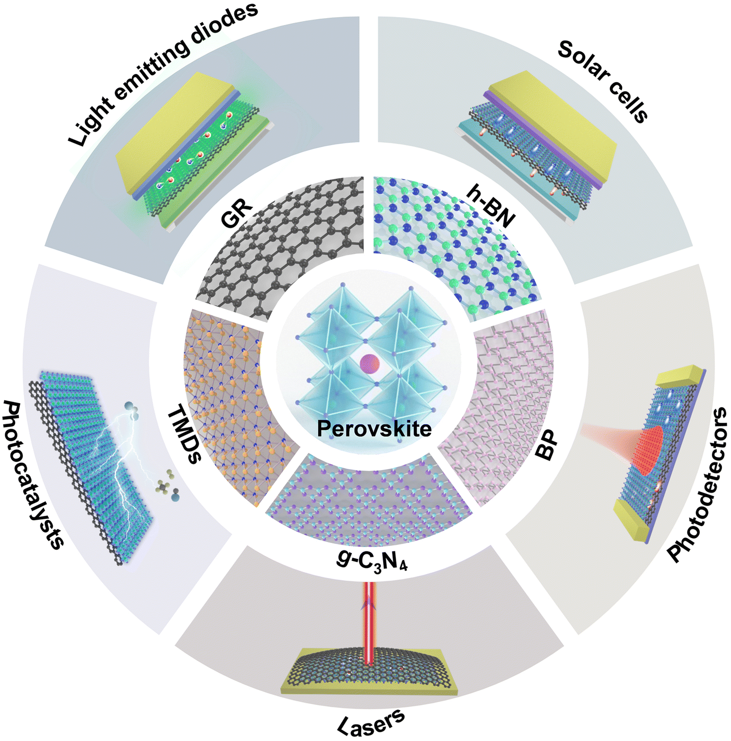 | ||
| Fig. 2 Schematic illustrations of the interfacial engineering of HPs and 2D materials (G, TMDs, BP, g-C3N4 and h-BN) for applications in LEDs, solar cells, photodetectors, lasers and photocatalysts. | ||
2. The structure and surface of HPs and 2D materials
The individual characteristics of HPs and 2D materials have a significant bearing on the design and construction of their interfaces. In this section, the crystal structures and surface properties of HPs and 2D materials, which are essential for the controllable preparation and modification of their hybrid interfaces, are discussed in detail.2.1. Crystal structures of HPs and 2D materials
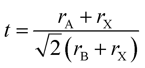
HPs and 2D materials have received significant attention owing to their excellent electronic and optical properties, which are closely related to their crystal structures.74,75 In particular, the formation and migration of photon- or electron-generated carriers are highly dependent on the way their atomic lattices twist and turn. The exploration of these unique properties is still ongoing and a study of the crystal structures of HPs may enhance the understanding of surface physics and chemistry.where rI (I = A, B, or X) refers to the ionic radii of each site (A, B, or X). Fluctuant t values of 0.77–1.10 indicate stable HPs. A slight change in the lattice symmetry and lattice parameters may occur with cation or anion substitution. In an ideal cubic HP, a unit cell contains A cations at the corners, B cations at body-centered positions and X anions at face-centered positions. The B cations unite with six adjacent X anions to form BX6 octahedrons. These octahedrons may experience lattice distortions owing to a size mismatch between the altering cations and anions, which can trigger the formation of derivative structures (i.e., double perovskite structures). The t values of typical lead-containing HPs are shown in Fig. 3a (right) with universal A-site cations and X-site anions. The t value exhibits an increasing trend accompanied by a decrease in the ionic radii at the X-sites, whereas a contrary tendency occurs at the A-sites. This result confirms the suitability of the empirical equation. Exploring the structural features can improve the understanding of the intrinsic performances of HPs and possibly allow high-throughput calculations for designing specific structures for practical applications.
 | ||
| Fig. 3 Crystal structure of (a) HPs, where A-sites can be occupied by Cs+, MA+, FA+ and Rb+, B-sites can be occupied by Pb2+, Sn2+, Cd2+ and Bi3+, X-sites can be occupied by Cl−, Br− and I− (left). Tolerance factor of various HPs for different A-sites (right), (b) G, (c) TMDs, (d) BP, (e) g-C3N4 of s-triazine (left) as well as tri-s-triazine (right) and (f) h-BN. | ||
Graphite oxide (GO) is a derivative of G that can be uniformly dispersed in aqueous solutions. GO is commonly prepared using the method developed by Hummer, wherein G is treated with strong acids and oxidizing agents.93 GO retains the layered structure of G with a net formula of C2O, wherein oxygen functional groups are introduced on each layered sheet. Adjacent GO layers are connected by weak interlayer van der Waals interactions, as well as through hydrogen bonding that originates from trapped water molecules. Owing to the presence of these attractive functional groups, GO is highly compatible with solution-based processes and can be used to fabricate large area high-quality films, which is beneficial for commercial applications.
Reduced graphene oxide (RGO), which is obtained through the chemical reduction of GO, is another important derivative of G. The oxygen-containing functional groups in GO are partially or entirely removed, making RGO more chemically inert. In addition, RGO possesses better electrical conductivity and higher transparency than GO, with various potential applications in optoelectronic devices.94,95 Although the graphene-like structure in RGO is destroyed after oxidation and reduction, the facile solution processability enables easy preparation of films.
Black phosphorus (BP). BP is an allotrope of phosphorus. It exhibits a puckered orthorhombic layered structure with a Cmca (64) space group. Monolayer BP is characterized by a puckered honeycomb structure, where one P atom is covalently bonded with three other atoms. These four P atoms are distributed across two parallel planes, with three atoms on one plane connected to the fourth atom on another plane (Fig. 3d). Adjacent layers are stacked together through a van der Waals force with a distance of 5.4 Å between each layer. BP has a universal direct bandgap that varies from its bulk counterpart (0.3 eV) to a monolayer (2 eV). Owing to its small bandgap, BP can act as an interface layer that bridges the energy gap between two materials with different bandgaps, with significant potential in near-infrared (NIR) optoelectronic applications.
Graphitic carbon nitride (g-C3N4). g-C3N4 has a graphene-like structure, which can be regarded as an N-substituted G matrix via the sp2 hybridization of carbon and nitrogen atoms. Two types of crystal structures, s-triazine and tri-s-triazine, are discussed herein. The s-triazine structure is composed of a periodic array of s-triazine units, which contain periodic single-carbon vacancies, whereas tri-s-triazine is composed of tri-s-triazine subunits connected by planar tertiary amino groups and larger periodic vacancies (Fig. 3e). g-C3N4 has a suitable bandgap of approximately 2.7 eV and can absorb blue-violet light with wavelengths of less than 475 nm from sunlight. Owing to the effective activation of molecular oxygen, g-C3N4 is an excellent material for photocatalysis and photodegradation.
Hexagonal boron nitride (h-BN). h-BN, which is called white graphene, has a lattice structure that is nearly identical to that of G. Monolayer h-BN is made of hexagonal rings with alternating boron and nitride atoms, and two adjacent atoms are coupled via strong covalent B–N bonding (Fig. 3f). The weak van der Waals forces between the two layers can be easily broken and various approaches have been developed to achieve the monolayer exfoliation of h-BN from its bulk mass. Although h-BN is an insulator with a wide bandgap of 5.9 eV, its excellent chemical stability and atomically smooth surface make it an appealing candidate for use as a substrate or an encapsulating layer in the fabrication of optoelectronic devices.
As discussed above, it is clear that B-site cations in HPs are coupled with X-site anions to form BX6 octahedrons by ionic bonds and A-site cations are linked to BX6 octahedrons by noncovalent bonds, while 2D materials are covalently connected. BX6 octahedrons in HPs are typically corner, edge or face sharing, permitting sufficient rotation and distortion with soft lattices. In reality, the optical and electrical properties of HPs, including light absorbance, carrier separation and transfer, self-trapped state and electron-phonon coupling, are closely related to the characteristics of their crystal structures.103–106 As for 2D materials, their structure rigidities are a huge obstruction for spatial rotation due to the fact that atoms are covalently bonded. However, researchers have observed the transition from rigidity to flexibility when G is bended.107 This softening resulted from shear, slip and the onset of superlubricity between the atomic layers and corresponds to a gradual change in scaling power from cubic to linear. These soft characteristics for both HPs and 2D materials are significantly vital to the fabrication of flexible devices, holding the potential for utilization in wearable devices.108–114 The performance loss in HP- or 2D material-based photovoltaic devices caused by the nonradiative recombination of electrons and holes and energy barriers at the interface is inevitable, which is closely related to their crystal structures. To prohibit these recombination pathways, it is fundamentally important to understand the crystal nature of HPs and 2D materials, explore their surface physics and chemistry, and unravel the working mechanisms and interfacial engineering in HP/2D material heterostructures.
2.2. Surface physics and chemistry in HPs and 2D materials
Considering the crystal nature and extreme large specific surface of HPs and 2D materials, their attractive physical, chemical and electronic characteristics are uncovered with a wide range of applications in energy storage and conversion, catalysis and electronics/optoelectronics.115–120 Understanding the individual surface physics and chemistry in HPs and 2D materials is fundamentally important to design novel interfaces, reveal the modification of interfacial behaviors and fabricate desired device architectures. In this section, how individual surface properties aid in the construction of HP/2D materials is discussed in great detail.Studying light–matter interactions is a key requirement for modifying the performances of optoelectronic devices such as light-harvesting and light-emitting devices. Light is a fluctuating electromagnetic field and matter is made up of charged particles, so the interaction between light and matter is electromagnetic. HPs and 2D materials are all direct band gap materials to serve as competent light absorbers that could trigger the formation of carriers with adsorbed light in a specific range of wavelengths, enabling numerous practical applications in photodetection, photovoltaic and light-emitting fields.134–137 The light absorption ability of HPs and 2D materials is different. HPs are well known as fantastic active materials with high absorption coefficients, long diffusion lengths and low trap densities.138–140 It was reported that the optical gain coefficient of HPs is comparable to those of industrial gain materials such as GaAs.141 High transmittance with weak light absorption in 2D materials caused by low dimensionality severely hinders more versatile applications for achieving high optical gains. For instance, only 2.3% and 10% of the incident light could be adsorbed by monolayer G and MoS2 in the range of visible spectrum, respectively.62,142 Much effort has been devoted to enhancing the optical absorption of 2D materials, such as plasmonic hybridization and incorporation into a Fabry−Perot cavity.143–146 By enhancing the photonic scattering effect and plasmonic Purcell effect, or modulating the multiple internal reflection, enhanced Raman scattering and optical absorption are realized. The fabrication of HP/2D material interfaces is an effective approach to improve the optical gain of the light adsorbed layer, enhancing the photocurrent and device performance.
Compared to conventional semiconductors, HPs possess a relatively low binding energy and more stable excitons at room temperature, enabling effective regulation of exciton–phonon coupling modes. Recently, researchers have investigated excitons that could be coupled to a series of phonons, and found that coupling modes are closely related to the species of organic cations and the thickness of inorganic layers.154 Signals of longitudinal optical phonons and longitudinal acoustic phonons have been observed by ultrafast transient absorption spectroscopy and resonant impulsive stimulated Raman spectroscopy.155,156 In addition, reduction of the molecular motion of HPs is appealing to reduce the interfacial exciton–phonon coupling and enhance device performances. As for 2D materials, each atom is covalently connected for a weak exciton–phonon coupling state. The artificial regulation of exciton–phonon coupling has been explored using spatial confinement or carrier localization effects.148,157,158 In brief, the exciton–phonon coupling in HPs and 2D materials could be rationally tuned to achieve abundant free excitons at the interface.
3. Construction, modification and property improvement of HP/2D material interfaces
Based on the crystal structures and the surface physics and chemistry of HPs and 2D materials discussed in Section 2, we explore the construction techniques of HP/2D material interfaces in this section. The synthetic strategies used to construct HP/2D material interfaces are designed based on the dimensions of the HPs and the interfacial engineering required to obtain a favorable bandgap alignment. Subsequently, the modified interfacial properties are discussed in detail.3.1. Architecture of HP/2D material interfaces
The design of HP/2D material interfaces is closely related to the interfacial properties and the device performances and consequently, the preparation of the HPs/2D materials is extremely important. The interfacial properties discussed herein primarily focus on the optical/electronic behaviors of carriers, which directly influence the performance of the resulting optoelectronic devices. Several key aspects must be carefully considered before constructing high-performance optoelectronic devices. First, the choice of HPs and 2D materials should be reasonable. There are several types of HPs and 2D materials, each with different characteristics that must be considered, with a particular focus on their bandgap structures. An unsuitable bandgap match between HPs and 2D materials can lead to carrier mobility disorders, which adversely affect the charge transport. Therefore, a reasonable combination of HPs and 2D materials is essential to obtain desirable properties. Second, the selected HPs and 2D materials should have a strong contact between them, as the distance between HPs and 2D materials influences the interfacial energy transfer. Finally, the type of heterointerface formed between HPs and the 2D materials should be designed carefully. The formation of the heterointerface is the origin of the modification of the carrier dynamics and the type of heterointerface should enhance the overall device performance.In this section, we summarize various recent approaches which were employed for preparing HP/2D material interfaces based on the morphological dimensions of HPs. Herein, we categorise HP/2D material interfaces into four types: zero-dimensional (0D) HP/2D material, one-dimensional (1D) HP/2D material, 2D HP/2D material and three-dimensional (3D) HP/2D material interfaces. The categorisation is mainly based on the coupling modes between HPs and 2D materials, which could be chemically bonded or physically connected. For 0D HP/2D material or 1D HP/2D material interfaces, HPs and 2D materials are typically connected by strong chemical bonds, while they are connected by weak van der Waals forces for 2D HP/2D material or 3D HP/2D material interfaces. Besides, the dimensions of HPs highly depend on their practical applications.159–166 For example, 1D HP nanorods are generally used in lasing devices. The nanorod structure works as an optical resonator to accumulate optical signals, thereby enhancing the quality of spontaneous emission.
 | ||
| Fig. 4 Synthesis of multi-dimensional HP/2D material interfaces. Preparation approaches of: (a) 0D HPs/2D materials (0D HPs: nanospheres or nanocubes); (b) 1D HPs/2D materials (1D HPs: nanowires); (c) 2D HPs/2D materials (2D HPs: nanoplates); (d) 3D HPs/2D materials (3D HPs: films). Graphene strands are depicted as the 2D material here to simplify the synthesis process. The carrier recombination and carrier separation and transfer occur simultaneously at the interface of the HPs and 2D materials. | ||
A precondition of using the lattice mismatching strategy is the existence of sufficient compatibility of lattice parameters between HPs and 2D materials. In addition, layered 2D materials possess two advantages: dangling-bond-free surfaces and flexibility, which permit HP seeds to nucleate and grow on the 2D material matrix. The smooth surface of 2D materials ensures that there is no obstruction to the entrance of the 0D HP precursor into the 2D materials. Furthermore, the flexibility of 2D materials ensures the release of the stresses built up during the incorporation of 0D HPs. Owing to the direct contact between the two materials, the interfacial transfer processes between 0D HPs and 2D materials are extremely rapid. As the crystal structures of the 0D HPs and 2D materials may differ, a nearly identical lattice parameter is required. For instance, a 0D MAPbBr3/MoS2 interface was achieved despite the differences between the crystal phases of the two components. MAPbBr3 quantum dots (QDs) were successfully grown on MoS2 nanosheets and the lattice mismatch between MAPbBr3/MoS2 was reduced to 1% with an optimized alignment. Improved energy transfer from MAPbBr3 to MoS2, with enhanced performance, was further realized in photodetectors.167 Other designs of 0D HP/2D material interfaces, such as MAPbBr3/G, MAPbBr3/GO, CsPbBr3/BP and γ-CsPbBr3/WS2, have been reported as well.168–174 Besides conventional lead HPs, the lead-free double perovskite structured Cs2AgBiBr6 was also coupled with RGO to achieve enhanced photocatalytic activity.175
The surface anchoring synthesis strategy is similar to the lattice mismatching strategy, but the lattice parameter requirements are not as strict as those in the latter. Typically, 2D materials are surface functionalized with organic ligands such as amino groups, carboxylic acid groups and sulfhydryl groups. The organic ligands on the surface of 2D materials actively adsorb lead ions and act as reaction sites for the nucleation and growth of 0D HPs. 0D HPs and 2D materials are chemically connected by ligand molecules, which trigger slower interfacial transfer processes than in 0D HP/2D material interfaces prepared using the lattice mismatching strategy. In addition, the increase in the carbon chain length of the ligand molecules further increases the difficulty of effective transport. In summary, the ligand molecules act as a bridge between the 0D HPs and 2D materials, and the carbon chain lengths of the ligand molecules determine the distance between the 0D HPs and 2D materials. For example, the edges of the heptazine units of porous g-C3N4 nanosheets were functionalized with abundant amino groups to guarantee strong interaction with CsPbBr3 QDs. The CsPbBr3/g-C3N4 interfaces exhibited good stability and outstanding photocatalytic properties under visible light irradiation.176 Surface functionalization is also possible for other 2D materials. Amino-functionalized CsPbBr3/h-BN interfaces exhibited improved stability against heat and demonstrated significant potential for application in white LED devices.177 Polyacrylic acid-grafted GO was used as a surface ligand to protect CsPbBr3 QDs and the resulting CsPbBr3/GO interfaces possessed excellent chemical stability in protic solvents.178 Other organic groups, such as sulfhydryl groups, can also be used as surface ligands. 4-Aminothiophenol functionalized MoSe2 was used as a template to grow CsPbBr3 QDs and the photocurrent of the resulting CsPbBr3/MoSe2 interface-based devices was promising.179 The introduction of surface halogen defects can also be used to effectively construct 0D HP/2D material interfaces. For example, the surface of RGO was treated with an aqueous solution of FeI2 to provide abundant active I-sites, which formed weak bonding interactions with the Pb-oleate precursors. The as-prepared α-CsPbI3/RGO interfaces exhibited enhanced stability and charge transport quality.180
Physical mixing is the easiest method of preparing 0D HP/2D material interfaces. The synthesis process is simple, as it involves the direct mixing of the as-prepared 0D HPs and 2D materials. The two materials overlap with each other at the resulting interface. However, owing to the weak interaction between the two materials, the interfaces prepared using this approach are less stable than those prepared using the lattice mismatching and surface anchoring strategies. Nevertheless, interfacial charge transfer still occurs. Considering the CsPbBr3/BP interface as an example, CsPbBr3 QDs were self-assembled on the surface of BP nanosheets after bath sonication treatment. The PL quenching of CsPbBr3/BP interfaces indicated the occurrence of charge transfer at the interface of the CsPbBr3 QDs and BP nanosheets.181 MAPbI3 coupled with RGO through physical mixing also exhibited outstanding photocatalytic properties.182
The processes used to transfer 1D HPs onto 2D materials include spin-coating and the pick-up and drop method. The spin-coating method is effective for dropping 1D HP precursor solvents onto 2D materials. 1D HPs are uniformly dispersed on 2D materials with the assistance of the centrifugal force and the residual organic solvents are removed after heat treatment. For example, G/CsPbI3 nanorod/G sandwich structures were constructed for weak coherent lasing applications. The CsPbI3 nanorods were fabricated by adding acetone to a CsPbI3 QD solution. Subsequently, a dispersion of CsPbI3 nanorods was spin cast onto the G layer at a speed of 2000 rpm for 20 s. Finally, the bottom G layer was transferred onto the CsPbI3 nanorods.192 MAPbBr3 nanorods were also coupled with a G layer using this synthesis strategy.193 Although the pick-up and drop method is more complicated, it provides precise control. The as-prepared 1D HPs are picked up by a stamp after heat and cooling treatment, then precisely dropped onto the selected 2D material. For example, CsPbBr3 nanorods were synthesized using methyl cyanide as an antisolvent. The target CsPbBr3 nanorods were then kept in contact with a stamp, which could pick up the CsPbBr3 nanorods after the heat and cooling treatment. Finally, the selected CsPbBr3 nanorods were dropped onto WS2 nanosheets.194
2D HPs are commonly prepared using a solvothermal approach or the chemical vapor deposition (CVD) method. The solvothermal approach is simple and convenient, as all the reagents are poured into a flask before subjecting them to heat treatment. The reaction occurs over several minutes without the protection of a N2 atmosphere. For example, SnO powder, hypophosphorous acid (H3PO2), hydroiodic acid (HI) and C6H5C2H4NH3I (PEAI) powders were mixed in a flask and heated to 150 °C with constant magnetic stirring. 2D (PEA)2SnI4 plates were formed after the solution was left to naturally cool to room temperature for 10 min.195 The CVD method is a convenient method for growing high-quality plates. Well-mixed powders with certain molar ratios are heated in a tube furnace. Gaseous precursors react to form HPs owing to the high temperature environment, which exceeds the melting point of the powders. The 2D HPs are finally deposited on the surface of suitable substrates. For instance, a mixture of PbI2 and CsI powders with a molar ratio of 1:1 was placed at the center of a tube furnace. The furnace temperature was set to a target temperature of 540 °C and the growth time was 10 min. 2D CsPbI3 plates were eventually deposited on substrates in a protective atmosphere of highly pure N2.196 A combination of the solvothermal and CVD methods has also been used to synthesize 2D MAPbI3 plates. PbI2 powder was first heated and then cooled to obtain a saturated PbI2 solution. The cooled PbI2 solution was then drop-cast onto the target substrate to precipitate 2D PbI2 nanosheets using air blowing. Finally, MAI powder was vaporized at 120 °C and reacted with the PbI2 substrate to generate 2D MAPbI3 plates.197
Owing to their similar flake structures, 2D HPs and 2D materials can be vertically arranged to form 2D HP/2D material interfaces or 2D material/2D HP interfaces. The transfer process of 2D HPs onto 2D materials or of 2D materials on to 2D HPs is identical, using a viscoelastic stamping method. For example, the as-prepared 2D (PEA)2SnI4 flakes were first exfoliated onto a polydimethylsiloxane (PDMS) stamp. The 2D (PEA)2SnI4/PDMS was then kept in contact with Au electrodes to release the PDMS stamp. This procedure was also used to fabricate 2D MoS2/Au. Finally, the 2D (PEA)2SnI4/Au was brought into contact with MoS2/Au to form a (PEA)2SnI4/MoS2 heterointerface.195 Similarly, 2D h-BN flakes were also transferred onto 2D CsPbI3 flakes using an all-dry PDMS stamp.196
3.2. Electronic energetics tuning of HP/2D material interfaces
As discussed above, morphologically dependent carrier behaviors are changed with different coupling modes. Besides, the energy-level alignment between HPs and 2D materials plays the leading role in affecting the interfacial optical/electronic properties. Numerous approaches have been developed to modify the band gap structures of HPs and 2D materials for achieving desired interfacial properties. In this section, we summarize the energy-level alignment and interfacial electronic energetics tuning of HP/2D material interfaces.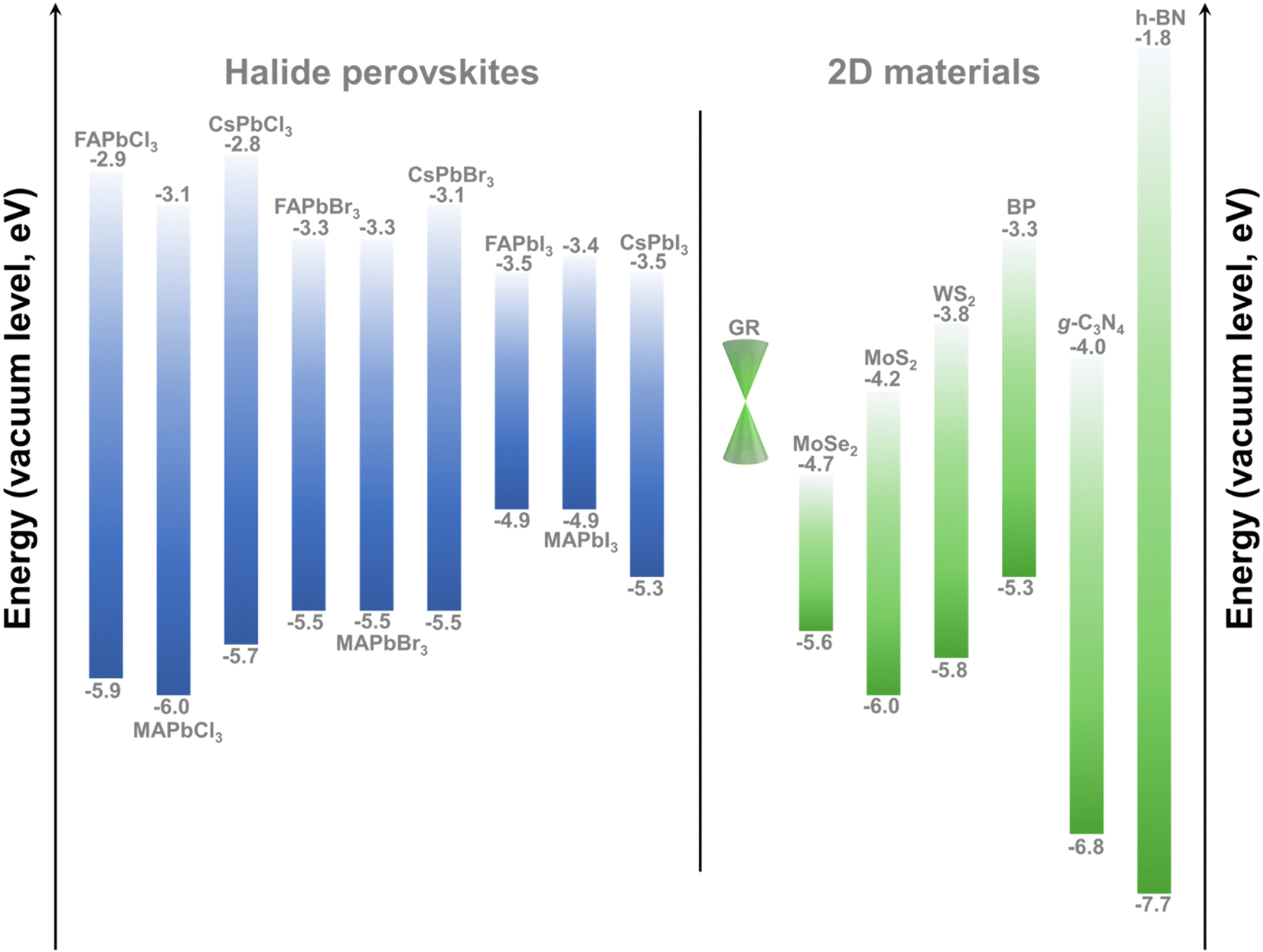 | ||
| Fig. 5 Band structures of HPs with different A sites and halogen species (left) and some bandgap matching 2D materials (right). | ||
The heterointerfaces of HP/2D material interfaces can be categorised into type I, type II and type III heterointerfaces, which have a significant influence on their interfacial behaviors. The type III heterointerface does not affect the carrier recombination or charge transfer between HPs and 2D materials, and has a limited effect on the device performance. Therefore, we only discuss type I and type II heterointerfaces herein. The defining feature of type I heterointerfaces is that component which possesses a higher conduction band offset (CBO) and a lower valence band offset (VBO), such as in CsPbBr3/BP. The electrons and holes in type I band alignment are simultaneously injected into a single component for effective carrier recombination, which triggers bright fluorescence with applications in lighting devices. The defining feature of type II heterointerfaces is that component possessing a higher CBO and VBO than the other component, but the VBO is lower than the CBO of the other component, such as in CsPbI3/g-C3N4. This band alignment accelerates the separation of electrons and holes, and offers significant potential for application in photovoltaic devices and photocatalytic applications. Owing to the component-tunable, thickness-dependent and dangling-bond-free characteristics of HPs and 2D materials, respectively, their bandgap structures can be easily modified to obtain a desired combination.
 | ||
| Fig. 6 Electronic energetics tuning of HPs/2D materials interfaces by (a) thickness regulation, (b) molecular functionalization and (c) chemical doping approaches, and their corresponding bandgap structures are shown in d–f. | ||
3.3. Optoelectronic regulations of HP/2D material interfaces
HPs and 2D materials have tunable bandgaps that enrich their electronic structures and permit the fabrication of various HP/2D material interfaces with desirable interfacial characteristics. As discussed in Section 3.2.1, the type of heterointerface of the HP/2D material interfaces is the key to adjust the interfacial properties. Therefore, while constructing HP/2D material interfaces, the bandgap energy level should be designed such that it accelerates exciton recombination or charge separation and transfer. Interfacial engineering offers significant potential for electronic modification and substantially expands the potential optoelectronic device applications. | ||
| Fig. 7 Interfacial properties of HP/2D material interfaces, including (a) light absorbance, (b) carrier recombination, (c) PL quenching and (d) TRPL decay. Carrier recombination induced by light irradiation accelerates the formation of excitons, whereas charge separation and transfer suppress carrier recombination. | ||
PL quenching. PL emissions from HPs primarily occur during free electron transition from the ground state to the excited state when exposed to an external light source; the related processes are the absorption of light, energy transfer and fluorescence. The strong fluorescence of HPs can be attributed to the violent recombination of photo-induced electrons and holes. However, fluorescence is quenched considerably in type II HP/2D material heterointerfaces.
This is because HPs and 2D materials have matched positions of conduction and valence band edges and excited electrons from the HPs rapidly transfer to the 2D materials through the CBO. This process significantly weakens the recombination of electrons and holes in HPs, inducing fluorescence quenching (Fig. 7c).
TRPL decay. TRPL decay is a profound measurement for monitoring the recombination dynamics of electrons and holes. The TRPL decay of HPs can usually be fitted with exponential curves that correspond to a fast decay τ1 and a slow decay τ2. The fast decay τ1 can be attributed to the trap-mediated nonradiative recombination caused by many-body effects, whereas the slow decay τ2 can be attributed to exciton radiative recombination. The average lifetime of HP/2D material interfaces is shorter than that of pure HPs, which suggests that the number of decay channels increases and carrier extraction is enhanced. The decreased PL lifetime at HP/2D material interfaces is identical to the PL quenching shown in Fig. 7c, which depicts the transfer of photogenerated carriers from HPs to the 2D materials (Fig. 7d). These two phenomena verify that effective charge separation and transfer can be achieved by incorporating 2D materials in HPs.
| Categories of HP/2D materials | Type of stability | Parameters | Values | Ref. |
|---|---|---|---|---|
| MAPbI3/BP | Thermal stability | PCE | 80% (100 °C, 24 h) | 241 |
| MAPbI3/G | Thermal stability | PL intensity | 70% (150 °C, 120 min) | 197 |
| MAPbI3/G | Thermal stability | PCE | 86% (150 °C, 30 min) | 242 |
| Cs0.05(MA0.17FA0.83)0.95Pb(I0.83Br0.17)3/G | Thermal stability | PCE | 90% (85 °C, 500 h) | 207 |
| MAPbI3/G | Photostability (50% RH) | J SC | No obvious change | 217 |
| PCE | No obvious change | |||
| MAPbI3/RGO | Photostability | PCE | 19% (120 h) | 209 |
| MAPbI3/RG | Photostability (65% RH) | PCE | 80% (30 d) | 243 |
| MAPbI3/G | Photostability (N2, RT) | PCE | 93% (30 h) | 244 |
| MAPbI3/FRGO | Photostability (under ambient conditions) | PCE | 70% (30 d) | 245 |
| CsPbBrxI3−x/G | Photostability | Photocurrent | 95% (37 h) | 246 |
| γ-CsPbI3/I−-RGO | Photostability (4 °C, 1% RH) | PLQY | 79% (4 week) | 174 |
| MAPbI3−xClx/RGO | Photostability (50% RH) | V oc | Almost unchanged (100 h) | 72 |
| MAPbI3/BP | Photostability (N2, 20% RH) | PCE | 94% (1000 h) | 247 |
| CsPbI3/h-BN | Moisture stability (in water) | Output intensity | 24 h | 196 |
| MAPbI3/CNT@G | Moisture stability (30–50% RH) | PCE | 80% (500 h) | 248 |
| γ-CsPbI3/RGO | Moisture stability (in water) | PLQY | 70% (4 week) | 249 |
| MAPbI3/MoS2 | Mechanical stability (radius: 5 mm) | Photocurrent ratio | 91% (20000 times) | 250 |
| FAPbI3−xBrx/AuCl3-G | Mechanical stability (radius: 12 mm) | PCE | No significant change (100 times) | 218 |
| MAPbI3/G | Mechanical stability | PCE | 86% (1000 times) | 251 |
| MAPbI3/G | Mechanical stability (radius: 1.75 mm) | PCE | 86% (500 times) | 252 |
| MAPbI3/G | Mechanical stability (radius: 2 mm) | PCE | 85% (500 times) | 253 |
| MAPbBr3/G | Mechanical stability (radius: 7.5 mm) | J SC | 81% (1200 times) | 214 |
| MAPbI3/MoS2 | Long-term stability | PCE | 86% (300 h) | 254 |
| MAPbI3/MoS2 | Long-term stability (20 °C, 20% RH) | PCE | 86% (20 d) | 236 |
| MAPbI3/MoS2:RGO-HS | Long-term stability | PCE | 91% (1032 h) | 124 |
| MAPbI3−xClx/MoS2 | Long-term stability | PCE | 90% (48 h) | 255 |
| MAPbI3−xClx/MoS2 | Long-term stability (15 °C, 20–45% RH) | PCE | 78% (56 d) | 256 |
| MAPbBr3/G | Long-term stability | Photocurrent | 6 mo | 71 |
| PLQY | 6 mo | |||
| Cs0.05(MA0.17FA0.83)0.95Pb(I0.83Br0.17)3/G | Long-term stability (under ambient conditions) | PCE | 88% (500 h) | 257 |
| MAPbI3−xClx/GO-NH3 | Long-term stability (under ambient conditions) | PCE | 72% (96 h) | 219 |
| (PEA)2PbI4/G | Long-term stability | Photocurrent | No obvious change (75 d) | 258 |
| MAPbI3/GO | Long-term stability (N2) | PCE | 80% (2000 h) | 259 |
| (BA)2(MA)n−1PbnI3n+1/h-BN/G | Long-term stability (N2) | Responsivity | 96% (400 h) | 211 |
| CsFAMAPbI3−xBrx/G | Long-term stability (50% RH, RT) | PCE | 94% (30 d) | 260 |
| MAPbI3/G | Long-term stability (under ambient conditions) | Photocurrent | 98% (20 d) | 249 |
| MAPbI3/AuCl3-G | Long-term stability (N2) | PCE | 70% (30 d) | 216 |
| MAPbI3/G-F | Long-term stability (50% RH, RT) | PCE | 82% (30 d) | 198 |
| MAPbI3−xClx/g-C3N4 | Long-term stability (under ambient conditions) | Photocurrent | 66% (7 d) | 239 |
| MAPbI3/MoS2 | Long-term stability | PCE | 91% (550 h) | 261 |
| MAPbI3/BP | Photocatalytic stability | HER rate | No obvious decline (100 h) | 262 |
| CsPbBr3/h-BN | Thermal stability | PL intensity | 74% (heat recycle) | 263 |
| Moisture stability | PL intensity | 72% (110 h) | ||
| CsPbBr3/GO | Thermal stability | PLQY | 77% (85 °C, 5 min) | 178 |
| Moisture stability | PLQY | 70% (12 h) | ||
| CsPbBr3/h-BN | Thermal stability | PL intensity | 80% (120 °C) | 177 |
| Long-term stability | PL intensity | 90% (22 d) | ||
| CsPbX3/h-BN | Thermal stability | PL intensity | 50% (120 °C) | 264 |
| Photostability | PL intensity | 70% (84 h) | ||
| Moisture stability (80% RH) | PL intensity | 60% (12 h) | ||
| MAPbI3/MoS2 | Mechanical stability (radius: 4 mm) | Photocurrent | 57% (3000 times) | 264 |
| Long-term stability (N2, 25 °C, 30% RH) | Photocurrent | 62% (30 d) | ||
| MAPbI3/MoS2 | Mechanical stability (radius: 4 mm) | Responsivity | 80% (1000 times) | 265 |
| Long-term stability (N2, 25 °C, 30% RH) | Responsivity | 78% (30 d) | ||
| FAPbI3−xBrx/TFSA-G | Photostability (60 °C, 30% RH) | PCE | 95% (1000 h) | 221 |
| Mechanical stability | PCE | 85% (5000 times) | ||
| MAPbI3/G | Photostability | PCE | 87% (500 h) | 266 |
| Mechanical stability | Sheet resistance | No obvious change (10000 times) |
The accumulation of heat during the operation of an optoelectronic device is inevitable. Continuous exposure to a thermal field triggers the agglomeration of small grains in HPs and significantly degrades their optoelectronic properties. Therefore, sufficient heat transfer from HPs is essential to eliminate the performance loss due to local overheating. 2D materials, such as G and h-BN, have high thermal conductivity and can provide efficient heat dissipation. For example, CsPbBr3 QDs were successfully coupled with exfoliated h-BN using a one-pot in situ method; the resulting interface had a PL intensity that was almost six times higher than that of pure CsPbBr3 QDs at 100 °C.177 The improved thermal stability can be attributed primarily to the intrinsic super-high thermal conductivity of h-BN, which promotes heat transfer from HPs to the h-BN, thereby suppressing heat accumulation (Fig. 8a). Therefore, local overheating of HPs can be eliminated by ensuring that a high thermal gradient exists between the 2D material and the HPs.178,196,197,263,264
 | ||
| Fig. 8 Stability improvements in HPs after incorporating 2D materials. (a) Stability against heat during heat build-up at the HP/2D material interfaces. The red arrows represent the directions of heat transfer along the surface of the 2D materials. (b) Stability against irradiated light. (c) Stability against moisture. The red arrows indicate that H2O molecules cluster to form a ball, demonstrating the enhanced hydrophobicity at the HP/2D material interfaces. (d) Stability against mechanical stress. The red arrows demonstrate the increase in the flexibility of the HPs owing to the mechanical behavior of the 2D materials. G is used as a representative 2D material in this figure. | ||
Photostability is an important parameter for evaluating the performance of optoelectronic devices. The etching of HPs under exposure to light is a slow process and the crystal structure of HPs is destroyed by extended exposure to light. Notably, the study of the light-related decomposition of HPs is attractive and the associated mechanism has been proposed.275–283 As for mixed halide or/and mixed cation perovskite compositions, it is generally believed that the phase segregation of HPs causes performance loss, which induces an increase in the number of Cs-rich clusters under illumination. Theoretical calculations suggest that light-generated carriers provide the thermodynamic driving force for phase segregation.284 As for single cation and single halide compositions, such as MAPbI3, the released proton from the MA under illumination is the main reason for the decomposition products of MeNH2, HI, and/or iodine.285 In a word, the illumination leads to the segregation of HPs and generates recombination centers which may cause a loss in the device performance. The incorporation of 2D materials ensures the effective extraction of light-generated carriers. The rapid segregation and transfer of carriers hinders the generation of Cs-rich clusters and the device performance remains stable under optical radiation conditions (Fig. 8b).
The stability of HPs against moisture has received significant research attention owing to the low tolerance of ionic crystals to polar solvents and especially to H2O molecules. The etching process of H2O molecules first triggers an increase in the number of surface defects, then collapses the crystal structures of the HPs. Organic ligands with longer carbon chains can protect HPs and offer excellent resistance to H2O molecules. However, organic ligands can hinder carrier behavior. To achieve sufficient charge injections in optoelectronic devices, a suitable balance must be achieved between device performance and moisture stability. The insertion of 2D materials, which have outstanding chemical and oxidation resistance, provides an elegant solution for waterproofing HPs.196 The hydrophobicity of HP/2D material interfaces is higher than that of pure HPs, as demonstrated by the larger contact angles of water droplets with the former (Fig. 8c).245 This can be attributed to the easy functionalization of 2D materials for providing effective protection against H2O molecules.
Flexible optoelectronic devices are suitable for wearable applications owing to their excellent ductility and transparency. The required flexibility is an important consideration in the fabrication of large-area HP films. Owing to the superior mechanical strength of 2D materials, HP/2D material interfaces have a significantly higher stability under mechanical stress than pure HPs. Soft and flexible 2D material-based substrates can protect HP films from damage (Fig. 8d). The construction of flexible films is an increasingly ubiquitous trend in the manufacturing of next-generation optoelectronic devices. Besides these four aspects of stability, the long-term stability at HP/2D material interfaces must be considered as well. Long-term stability is the continuous resistance of the structure to complex external environmental factors. The major difference between long-term stability and other stabilities is that long-term stability refers to the stability under direct exposure to the external environment during testing process, but other stability tests are under specific conditions, such as inert gas protection or specific humidity. In a word, the long-term stability is more convincing for evaluating practical device performance. As there are no intrinsic differences between long-term stability and the other types of stability, long-term stability is not discussed herein.
4. Prospective applications based on HP/2D material interfaces
In this section, we discuss the optoelectronic applications of HP/2D material interfaces with different interfacial properties. HP/2D material interfaces either have type I or type II heterointerfaces, which exhibit different aligned energy levels. The type I heterointerface is beneficial for carrier recombination, demonstrating excellent potential for lighting applications, such as in LEDs. The type II heterointerface promotes effective charge separation and transfer, offering significant potential for photovoltaic and photocatalytic applications, such as in solar cells, photodetectors, lasers, the hydrogen evolution reaction (HER) and carbon dioxide (CO2) reduction. Furthermore, the prospective applications of HP/2D material interfaces are discussed as well to provide future research directions for the development of HPs and 2D materials.4.1. LEDs
HP-based LEDs are promising candidates for next-generation lighting applications owing to their advantages of easy fabrication, high brightness and broad color gamut.286–292 The EQE values are rapidly improved, reaching a value of 9.5% even for blue LEDs.293 In 2021, the EQE of blue LEDs reached an unprecedented value of 12.6% using an interfacial nucleation seeding strategy.230 Although further increases in the efficiency of LEDs are challenging, new device structures can be designed to realize more efficient conversion. Owing to the excellent photoelectric properties of 2D materials, HP/2D material interfaces have significant potential for achieving interfacially enhanced performance.Organic/inorganic hybrid perovskites (OIPs) have several desirable characteristics for application as light-emitting layers in LEDs. However, they have several intrinsic problems, including a long exciton diffusion length and a small exciton binding energy, which severely limit their EL intensity. To eliminate carrier transfer obstructions, four-layer G films were employed as the anode with a self-organized gradient buffer hole-injection layer.214 The device structure of LEDs with G electrodes and an MAPbBr3 emitter is shown in Fig. 9a (left). Its layered structure was confirmed using cross-sectional scanning electron microscopy (SEM). The resulting MAPbBr3/G LEDs had a brighter luminance and higher device efficiency (EQEmax = 3.8%) than the MAPbBr3/ITO LEDs (EQEmax = 2.2%). This improvement can be attributed primarily to the elimination of exciton quenching in the ITO electrode due to the migration of In and Sn species (Fig. 9a, right). Furthermore, G-based LEDs have better flexibility, resulting in significant advances in the design of flexible optoelectronic devices.
 | ||
| Fig. 9 HP/2D material based LED devices with improved stability and luminescent properties. (a) Device structure of LEDs with G electrodes and MAPbBr3 emitter (left) and its luminance at different current densities compared to that of ITO-based LEDs (right). Reproduced from ref. 214. Copyright 2017 Wiley-VCH Verlag GmbH & Co. KGaA, Weinheim. (b) Schematic illustration of the device architecture of LEDs with the BP hole injection layer and CsPbBr3 emitter (left), and EQE characters with or without the BP layer (right). Reproduced from ref. 234. Copyright 2019 Wiley-VCH Verlag GmbH & Co. KGaA, Weinheim. (c) Schematic illustration of enhanced stability of CsPbBr3-based LEDs with a protective h-BN layer against heat and moisture. Reproduced from ref. 263. Copyright 2019 American Chemical Society. (d) CIE diagram of CsPbX3/h-BN-based LEDs. The color gamut (orange hexagons) is 125% of the NTSC standard (black dots) and its color coordinate is (0.372, 0.322) (white hexagon). Reproduced from ref. 177. Copyright 2019 The Royal Society of Chemistry. | ||
Inorganic HPs can also be used for lighting applications. However, their lower energy levels limit the effective transfer of the photogenerated carriers, which significantly weakens their optoelectronic performance. To overcome the large hole injection barriers and high leakage current in LEDs, exfoliated BP flakes with fewer defects can be integrated as a hole-injection layer.234 The device architecture of LEDs with a BP hole-injection layer and a CsPbBr3 emitter is depicted (Fig. 9b, left). The BP interlayer lowers the injection barrier between PEDOT:PSS and CsPbBr3, which triggers a slight enhancement in the PCE. In addition, the incorporation of BP promotes the growth of high-quality CsPbBr3 films. A CsPbBr3 film coated directly on PEDOT:PSS demonstrated a high density of pinholes, whereas a CsPbBr3 film deposited on a BP interlayer exhibited a smooth and uniform morphology with a low pinhole density. The decrease in the pinhole density reduces the current leakage from the LEDs. Consequently, the EQE of the BP-incorporated LEDs increased to 2.8%, whereas that of the BP-free LEDs was only 0.7% (Fig. 9b, right).
In addition to the improved EQE, the stability of HPs in LED devices can be enhanced by constructing HP/2D material interfaces. h-BN is widely used to stabilize HPs owing to its superior heat conductivity and excellent chemical stability, which significantly increases the heat and moisture resistance of HPs (Fig. 9c).177,263 Besides the stability requirements, a wide color gamut is also necessary for the construction of white LEDs. For example, green CsPbBr3/h-BN was combined with a blue chip and red commercial phosphors to fabricate white LEDs. The realization of a wide color gamut was primarily attributed to the high color purity of CsPbBr3/h-BN, which resulted from the negligible loss of luminous performance owing to the presence of h-BN. The color coordinate of LEDs can be adjusted by modifying the proportion of each component. A wide color gamut of 125% of the National Television System Committee (NTSC) standard was achieved as shown in Fig. 9d. The fabricated LEDs possessed a warm light with the color coordinate at (0.372, 0.322), which is close to that of standard white light (0.33, 0.33).
HP/2D material interfaces also have excellent potential for application in displays. Micro-LEDs have attracted significant attention and are considered to be the future of displays. The diminutive matrix techniques of LEDs require a smaller micrometer size, which endows micro-LEDs with extremely high pixel densities. In addition, micro-LEDs have outstanding properties, including high brightness, high color saturation, low power consumption, long lifetime and rapid response, which are extremely desirable for display applications.294–297 However, mass transfer, which ensures the precise control of numerous RGB micro-LED unit arrays, is extremely difficult. It remains a significant obstacle to the practical application of micro-LEDs and must be resolved urgently. The use of HP/2D material interfaces as emitter layers in displays offers the following advantages: (1) the easy surface functionalization of 2D materials permits strong chemical combinations with HPs, which is beneficial for long-term stability as the resulting interfaces are protected from decomposition; (2) the high transparency of 2D materials can effectively maintain the optical properties of HPs; (3) flexible 2D material substrates are favorable for wearable displays; (4) HP/2D material interfaces could provide a possible solution to the mass transfer problem. A prospective HP/2D material interface used in a micro-LED display is depicted in Fig. 10. The HPs are combined with functionalized 2D materials to form a stable luminous unit (Fig. 10c). Color micro-LED units can be prepared by changing the species and ratio of halogens. The color micro-LED units are then transferred stepwise onto the as-deposited GaN film using elastomer PDMS transfer stamps, which form a weak van der Waals force with the 2D material to realize snatching and dropping. Periodical arrays of RGB micro-LED units can be used to construct a micro-LED chip, which functions as a pixel (Fig. 10b). A cross-sectional image of a micro-LED chip with SiO2 as the substrate, GaN as the excitation source, HP/2D materials as the emitter and a control circuit is shown in Fig. 10d. The color of each micro-LED chip can be adjusted by using different on/off ratios for each RGB micro-LED unit. A large-area micro-LED display can be fabricated using numerous well-organized micro-LED chips arranged against a backlight (Fig. 10a). Therefore, HP/2D material interfaces have the potential to promote the commercialization of micro-LEDs.
 | ||
| Fig. 10 Prospective HP/2D material interfaces used as the emitter in micro-LEDs for display applications. (a) The display screen consists of several micro-LED chips. (b) Schematic diagram of a single micro-LED chip; the HP/2D material interfaces are transferred to a GaN chip using a weak van der Waals force. (c) Magnified image of the HP/2D material interface; the surface of the 2D materials is functionalized with organic ligands to form strong chemical bonds with the HPs. (d) Cross-section of the micro-LED chip with the SiO2 substrate, GaN excitation source, HP/2D material interface emitter and the control circuit. | ||
4.2. Solar cells
The efficiency of PSCs has witnessed unprecedented growth, exceeding that of other types of solar cells. The photovoltaic function of organic–inorganic lead HPs was first reported in 2009.8 HP NCs were deposited on a TiO2 layer as visible-light sensitizers and a low PCE of 3.8% was obtained. In 2012, an impressive PCE of 9.7% was achieved for hybrid HPs that primarily originated from the use of a solid hole transport layer (HTL).298 In 2015, a PCE of 20.1% was reported for a PSC that was fabricated using a modified two-step method.299 In 2016, a triple-cation HP composition (FA/MA/Cs) was employed, resulting in an even higher PCE of 21.1%.300 In 2019, bilateral alkylamine treatment was used to suppress charge recombination, achieving a PCE of 22.6%.301 Recently, a record PCE of 25.8% was achieved via coherent interlayers on SnO2 electrodes.10 The pursuit of a further increase in PCE is underway. The typical structure of PSCs is glass/FTO/electronic transport layer (ETL)/perovskite/HTL/Ag, which can result in the separation and transfer of photo-induced carriers. The device architecture of PSCs is extremely important to their performance, and it can be broadly divided into mesoporous and planar (normal and inverted) devices. Since the discovery of single-layer RGO, 2D materials have been widely used in PSCs. A comprehensive review of the applications of 2D materials in PSCs was published recently.302 To avoid repetition, a brief depiction of the roles of 2D materials and the working mechanism of 2D materials considering interfacial performance modification is presented herein. A summary of the device performance and device structures of PSCs with HP/2D material interfaces is presented in Table 2.| Type of 2D material | Function | Device structures | PCE (%) | Ref. |
|---|---|---|---|---|
| G nanofiber | Additive | FTO/TiO2/MAPbI3:G/Spiro-MeOTAD/Au | 19.83 | 303 |
| N-RGO | Additive | FTO/c-TiO2/mp-TiO2/FA0.85MA0.15Pb(I0.85Br0.15)3:N-RGO/Spiro-OMeTAD/Au | 18.7 | 73 |
| BP QDs | Additive | Glass/ITO/PTAA/MAPbI3:BP/PCBM/BCP/Ag | 20 | 241 |
| BP | Additive | FTO/c-TiO2/SnO2/MAPbI3:BP/Spiro-OMeTAD/Ag | 20.23 | 247 |
| MoS2 | HTL | FTO/TiO2/MAPbI3/Spiro-OMeTAD:MoS2/MoO3/Ag | 20.18 | 254 |
| MoS2-PAS | HTL | ITO/PEDOT:PSS:MoS2/MAPbI3/PCBM/Ag | 16.47 | 224 |
| MoS2 | HTL | FTO/TiO2/MAPbI3−xClx/MoS2/P3HT/Au | 7.2 | 255 |
| MoS2 | HTL | ITO/MoS2/MAPbI3/PCBM/Al | 6.01 | 212 |
| RGO-PhOHex | HTL | Cs0.15FA0.85PbI3/P3HT:RGO-PhOHex | 9.8 | 222 |
| FRGO | HTL | ITO/ZnO/C60/MAPbI3/FRGO/PEDOT/MoO3/Ag | 14.9 | 245 |
| G | HTL | ITO/TiO2/MAPbI3/Spiro-OMeTAD/CNT@G/Au | 19.56 | 248 |
| RGO | HTL | ITO/RGO/Cs0.05(MA0.17FA0.83)0.95Pb(I0.83Br0.17)3/PCBM/BCP/Ag | 16.28 | 305 |
| MFGO | HTL | ITO/MFGO/MAPbI3/PC61BM/BCP/Ag | 14.7 | 313 |
| RGO | HTL | FTO/c-TiO2/nc-TiO2/MAPbI3/RGO/Au | 6.6 | 209 |
| GO-AuNP | HTL | ITO/GO-AuNP/MAPbI3/PCBM/BCP/Ag | 14.6 | 314 |
| BP | HTL | FTO/TiO2/MAPbI3/BP/Au | 16.4 | 315 |
| MoS2 | ETL | FTO/MoS2/MAPbI3/Spiro-OMeTAD/Au | 13.1 | 306 |
| NDI-G | ETL | ITO/NDI-G/SnO2/FA0.75MA0.15Cs0.1PbI2.65Br0.35/Spiro-OMeTAD/Au | 20 | 210 |
| G | ETL | FTO/ZnO/G/FA0.85MA0.15Pb(I0.85Br0.15)3/Spiro-OMeTAD/Au | 21 | 244 |
| G nanoribbon | ETL | FTO/G/c-TiO2/m-TiO2/MAPbI3/Spiro-OMeTAD/Ag | 17.7 | 304 |
| RGO | ETL | Glass/ITO/PEDOT:PSS/CH3NH3PbI3−xClx/PCBM:RGO/PFN/Ag | 14.5 | 72 |
| G QDs | ETL | FTO/c-TiO2/mp-TiO2:G/Cs0.05(MA0.17FA0.83)0.95Pb(I0.83Br0.17)3/Spiro-OMeTAD/Au | 14.36 | 257 |
| N-G | ETL | FTO/ZnO/ZnO:N-G/MAPbI3/Spiro-OMeTAD/Ag | 16.8 | 228 |
| GO-Li | ETL | FTO/c-TiO2/m-TiO2/GO-Li/MAPbI3/Spiro-MeOTAD/Au | 11.1 | 220 |
| G | Bottom | PEN/MoO3:G/PEDOT:PSS/MAPbI3/BCP/C60/LiF/Al | 17 | 253 |
| TFSA-G | Bottom | Glass/TFSA-G/PEDOT:PSS/FAPbI3−xBrx/PCBM/Al | 19 | 221 |
| G | Bottom | PET/G/P3HT/CH3NH3PbI3/PC71BM/Ag | 12 | 252 |
| G | Bottom | G/MoO3/PEDOT:PSS/MAPbI3/C60/BCP/LiF/Al | 14 | 251 |
| G | Bottom | Glass/G/PEDOT:PSS/MAPbI3/PCBM/Al | 18 | 217 |
| AuCl3-G | Bottom | PET/AuCl3-G/PEDOT:PSS/MAPbI3/PCBM/Al | 18 | 218 |
| G | Bottom | PES/G/NiOx/MAPbI3/PCBM/AZO/Ag/AZO | 14 | 266 |
| AuNPs-RGO | Bottom | Glass/AuNPs-G/c-TiO2/mp-TiO2/MAPbI3−xClx/Spiro-OMeTAD/Au | 0.62 | 316 |
| G | Bottom | G/MoO3/PEDOT:PSS/MAPbI3/C60/BCP/LiF/Al PEDOT:PSS/MAPbI3/C60/BCP/LiF/Al | 17.1 | 122 |
| N-G | Top | FTO/TiO2/MAPbI3/N-G | 10.3 | 308 |
| G | Top | FTO/SnO2/Cs0.05(MA0.17FA0.83)0.95Pb(I0.83Br0.17)3/Spiro-OMeTAD/G | 18.7 | 207 |
| N-G QDs | Interfacial | N-G/FTO/TiO2/γ-CsPbI3/PTAA/Au | 16 | 229 |
| G-NH3 | Interfacial | FTO/TiO2/MAPbI3/G-NH3/Spiro-OMeTAD/Au | 15 | 208 |
| G | Interfacial | Glass/FTO/TiO2/CsFAMAPbI3-−xBrx/CuSCN/G/Au | 15.8 | 260 |
| GO-NH3 | Interfacial | ITO/PEDOT:PSS/GO-NH3/MAPbI3−xClx/PCBM/Ag | 16.11 | 219 |
| G-F | Interfacial | Glass/ITO/PEDOT:PSS/MAPbI3/PCBM/G-F/Al | 14.3 | 198 |
| RG | Interfacial | FTO/TiO2/RG/MAPbI3/Spiro-OMeTAD/Au | 17.2 | 243 |
| BP QDs | Interfacial | ITO/PEDOT/BP/MAPbI3/PCBM/Ag | 16.69 | 309 |
| MoS2 RGO-HS | HTL Interfacial | Glass/FTO/c-TiO2/mp-TiO2/MAPbI3/MoS2/RGO-HS/Spiro-OMeTAD/Au | 20.12 | 124 |
| MoS2 TETA-G | ETL bottom | Glass/TETA-G/MoS2/MAPbI3/PTAA/Au | 14.27 | 265 |
| MoS2 G | ETL bottom | Glass/G/MoS2/MAPbI3/PCBM/BCP/Al | 13.09 | 317 |
| GO GO-Li | HTL ETL | FTO/GO/HPs/TiO2/GO-Li/Al | 10.2 | 311 |
| GO GO | Bottom additive | ITO/GO/MAPbI3:GO/PCBM/Ag | 15.2 | 259 |
 | ||
| Fig. 11 Typical device structures of solar cells with different HP species and 2D materials. (a) Device structure of the MAPbI3:g-C3N4-based solar cell: g-C3N4 acts as an additive, forming a high quality MAPbI3 film. Reproduced from ref. 123. Copyright 2018 Wiley-VCH Verlag GmbH & Co. KGaA, Weinheim. (b) Structure of MAPbI3/RGO-based solar cells: RGO works as an HTL to accelerate hole transfer. Reproduced from ref. 209. Copyright 2016 Elsevier Ltd. (c) Schematic structure of MAPbI3/G-based solar cells, wherein G is the bottom electrode. Reproduced from ref. 122. Copyright 2016 Wiley-VCH Verlag GmbH & Co. KGaA, Weinheim. (d) Schematic architecture of FA0.83MA0.17PbI2.63Br0.37/NDI-G-based solar cells, wherein G works as an ETL to accelerate electron transfer; the expanded scheme depicts the chemical structure of NDI and the bonding condition of NDI-G with perovskite films. Reproduced from ref. 209. Copyright 2016 Elsevier Ltd. (c) Schematic structure of MAPbI3/G-based solar cells, wherein G is the bottom electrode. Reproduced from ref. 210. Copyright 2018 American Chemical Society. (e) Device structure of Cs0.05(MA0.17FA0.83)0.95Pb(I0.83Br0.17)3/G-based solar cells, wherein G works as the top electrode. Reproduced from ref. 207. Copyright 2019 The Royal Society of Chemistry. (f) Schematic architecture of MAPbI3/NH3-G-based solar cells, wherein G works as an interfacial layer to protect the perovskite film from surface traps; the expanded scheme shows the bonding condition of NH3-G with perovskite films. Reproduced from ref. 208. Copyright 2016 The Royal Society of Chemistry. (g) Structure of MAPbI3/f-GO/MoS2-based solar cells, wherein two types of 2D materials work collaboratively to realize highly efficient solar cells; the expanded scheme shows the bonding condition of f-GO/MoS2 with perovskite films; f-RGO and MoS2 work as the interfacial layer and HTL, respectively. Reproduced from ref. 124. Copyright 2018 American Chemical Society. | ||
G and its derivatives are versatile and can be employed to achieve different functions.122,124,207–209 Although 2D materials, in whichever form, can achieve higher performance, their working mechanisms must be explored further. A comparison between the insertion locations of RGO was performed and the distinguishing performances were analyzed.310 Apart from the independent use of 2D materials as a single component in PSCs, numerous studies have focused on the hybrid combination of two 2D materials. A PSC with a hybrid combination of RGO as an interlayer and MoS2 as an HTL yielded a high PCE of more than 20% (Fig. 11g).124 The development of HP/2D material solar cells is still in its infancy and there is large space for improvement. Compared to the record PCE of 25.8% in PSCs, HP/2D material solar cells delivered a PCE of 21.0%, which was achieved by introducing monolayer G at the interface of the ZnO layer and HP layer.10,244 One should note that HP/2D material solar cells have many advantages such as enhanced optical absorption, improved crystallization and preferred orientation of HPs, improved morphology with nearly complete coverage, better matched energy-level-alignment and improved stability, which are closely related to device performances. The challenge for HP/2D material solar cells is how to balance the energy level and the thickness of layer transport, which originate from the negative correlations between the thickness and open-circuit voltage. To this regard, we envision that monolayer or nanosized 2D materials may further promote the PCE of PSCs. Therefore, the use of 2D materials offers significant potential for designing highly effective PSCs. Moreover, a variety of potential 2D material combinations offer infinite possibilities.259,265,311,312
4.3. Photodetectors
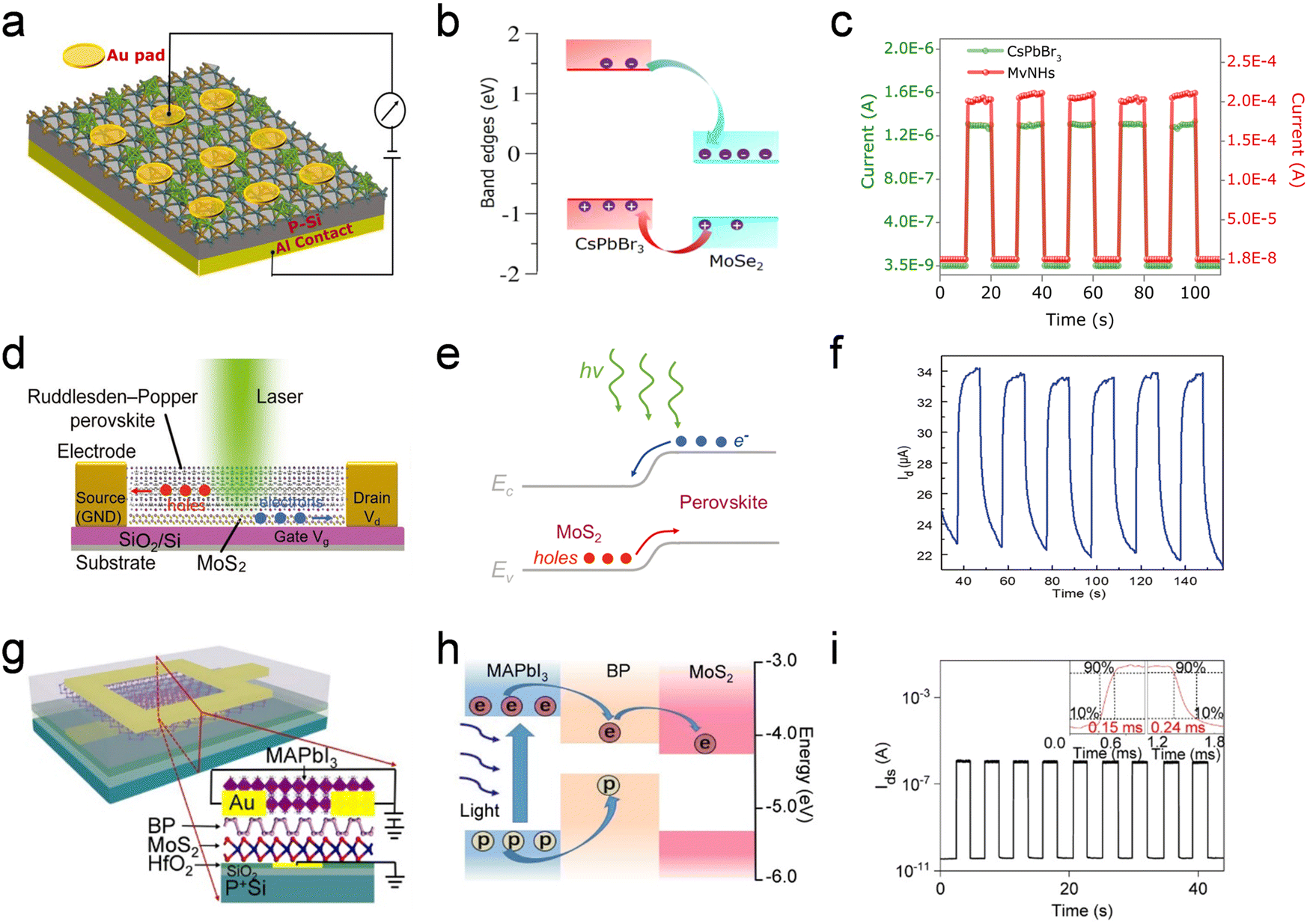
Photodetectors are optoelectronic devices that are used to convert optical signals into electrical signals under light irradiation. The parameters used to evaluate the performance of photodetectors primarily include the photocurrent, EQE, on/off ratio, response time, responsivity and detectivity.318–322 An ideal photodetector should satisfy all the related performance requirements; however, some contradictions exist for some performance parameters, such as the need to simultaneously maintain a high responsivity and a fast response time. Therefore, optimal light-absorbing and charge transfer layers must be selected to achieve high performance. Owing to their excellent light absorption coefficient, long charge carrier diffusion length and low-temperature synthesis, HPs are an attractive option for application in the light-absorbing layer. However, the response speed of HP-based photodetectors is limited by the long lifetime of the trapped carriers. 2D materials can be inserted to modify the interfacial properties, triggering the synergistic effect of the photogating mechanism and the modulation of Schottky barriers.323–325Various HP/2D material interfaces can be used to enhance specific performance aspects of photodetectors. A CsPbBr3/4-aminothiophnol MoSe2 interface was designed to overcome the distinguishable surface chemistry between two classes of materials (Fig. 12a). Close contact between the CsPbBr3 and MoSe2 layer was ensured by constructing a bridge that led to the formation of a donor–bridge–acceptor system, which facilitated faster charge diffusion across the CsPbBr3/MoSe2 interfaces (Fig. 12b). Consequently, the photocurrent of the interface was significantly higher than that of both the pure CsPbBr3 NCs and the pristine MoSe2 nanosheets (Fig. 12c).179 Phosphorus-doped g-C3N4, which has a reduced band gap owing to chemical doping, was coupled with MAPbClxI3−x to form a type-II heterointerface.239 The design of the interface promoted effective charge separation and transfer, significantly decreasing the dark current from 10−9 to 10−11, increasing the on/off ratio from 103 to 105 and enhancing the photo-detectivity by more than one order of magnitude. A vertical photodetector was fabricated combining the superior properties of MAPbBr3 QDs and G; the resulting device had a large photoresponsivity (>109 A W−1) and a fast response time (50 μs).71 Owing to the easy surface functionalization and chemical doping of G and its derivatives, well-aligned energy levels can be designed with a high carrier mobility.168,211,237,246,249,326–329 2D Ruddlesden–Popper HPs, which possess a relatively higher stability, were coupled with MoS2 to enhance light absorption and suppress charge recombination, with an additional RGO channel for favored charge transfer.195,235,330 The device architecture of an ultrathin 2D (BA)2PbI4/MoS2 interface is shown in Fig. 12d. The SiO2/Si substrate serves as a back gate and one Au electrode serves as the drain electrode. The schematic energy band diagram indicates that the (BA)2PbI4 layer effectively generated excitons under illumination; the electron–hole pairs are separated by the built-in electric field at the interface between (BA)2PbI4 and MoS2 (Fig. 12e). The ultrathin 2D (BA)2PbI4/MoS2 interface exhibited significantly higher photoresponsivity (six orders of magnitude) and detectivity (two orders of magnitude) owing to facile charge transfer (Fig. 12f).331 Other HPs have also been successfully combined with MoS2 to obtain high performances.167,199,223,250,332–334
 | ||
| Fig. 12 Photodetectors based on HP/2D material interfaces with enhanced interfacial charge separation and transfer. (a) Schematic illustration of the CsPbBr3/MoSe2-based photodiode. (b) Band alignment and charge transfer at the CsPbBr3/MoSe2 interface. (c) Optical switching characteristics of devices without or with MoSe2, which were recorded by switching the light source (100 mW cm−2) at a 0 V bias. Reproduced from ref. 179. Copyright 2020 American Chemical Society. (d) Schematic description of (BA)2(MA)n−1PbnI3n+1/MoS2-based photodetectors. (e) Energy band diagram of the (BA)2(MA)n−1PbnI3n+1/MoS2 interface. (f) Photo switching characteristics of the (BA)2(MA)n−1PbnI3n+1/MoS2 hybrid photodetector under alternating illumination ON and OFF. Reproduced from ref. 331. Copyright 2019 Wiley-VCH Verlag GmbH & Co. KGaA, Weinheim. (g) Schematic illustration of the MAPbI3/BP/MoS2-based photodetector. (h) Band diagram of MAPbI3/BP/MoS2 and photocarrier transfer under laser illumination. (i) Dynamic response of MAPbI3/BP/MoS2-based photodetectors. The inset shows the τrise (τdecay) value of the device recorded using an oscilloscope. Reproduced from ref. 337. Copyright 2019 American Chemical Society. | ||
WS2, when integrated with either 1D CsPbBr3 nanorods or MAPbBr3 films, suppresses the dark current and exhibits an ultrahigh on/off ratio and photo-detectivity.194,335 A Schottky barrier-controlled MAPbI3−xClx/BP photodetector was fabricated with ultrahigh sensitivity and a fast response speed.336 The incorporation of BP accumulated the electron detrapping process in MAPbI3−xClx under optical conditions. The exploration of the interfacial engineering between CsPbBr3 and BP demonstrated the repressive effect of surface ligands on charge transfer, which improved the understanding of the charge transfer process in multi-dimensional composites.169 Hybrid 2D materials, such as BP/MoS2, have tunable energy levels and can be used to achieve both fast response and high responsivity.337 Other types of 2D materials (WSe2 and MoSe2) have also been designed to accumulate the charge separation and transfer process and realize high-performance photodetectors.338–341 In addition to the utilization of single 2D materials, multicomponent 2D materials have been constructed by various scholars. A schematic diagram of a MAPbI3/BP/MoS2 photodetector is shown in Fig. 12g. The hybrid BP/MoS2 has a type II heterointerface, whereas MAPbI3/BP has a type II heterointerface (Fig. 12h). The photo-generated photocarrier diffused into the BP layer, which was followed by photocarrier separation and collection owing to the existence of a built-in electric field at the BP/MoS2 interface. The on/off switching characteristics of the MAPbI3/BP/MoS2 device exhibited good reliability and fast on/off switching repetition in multiple-cycle tests (Fig. 12i). The high-resolution temporal photoresponses of τrise and τdecay were 150 μs and 240 μs, respectively. This indicates that the response speed of the MAPbI3/BP/MoS2 device is much faster than that of conventional photogate devices.337
The stability issues of HP-based photodetectors can also be modified by introducing 2D materials. A MAPbI3−xClx/BP-based photodetector exhibited excellent stability under a light source that was switched on and off multiple times.336 The stable photocurrent suggested that the device had outstanding reproducibility. The power-dependent fittings of the EQE, photoresponsivity and detectivity were exponential, which can be attributed to the higher possibility of scattering and recombination under stronger illumination.
NIR photodetectors have several promising optoelectronic applications with a wide range of civil and military uses.342–345 The collection and utilization of unobservable NIR signals are extremely valuable for numerous practical applications. The most commonly used NIR-sensitive materials are PbS, PbSe and InSb, which trigger a change in conductivity when exposed to NIR radiation; however, they have some drawbacks.134,346,347 For instance, thermal sources and light interfere with NIR signals, inducing a decline in responsivity and detectivity. Therefore, the exploration of highly stable materials that are sensitive to NIR is an urgent requirement. Recent studies have shown that organic–inorganic HPs have excellent potential for application in NIR photodetectors.348–351 A MAPbI3-based photodetector exhibited an ultrabroadband photoresponse ranging from UV to terahertz (THz) at room temperature.352 This exciting phenomenon affirms the possibility of using HPs as NIR absorbing layers. Although HP-based NIR photodetectors are imprudent and unviable for practical use currently, we believe that HPs can be used to improve the performance of NIR photodetectors in the future. A prospective HP/G-based NIR photodetector is shown in Fig. 13. It comprises an underlying HP layer and a 2D material layer that function as a light-absorbing layer and a charge-transfer layer, respectively. Owing to the unprecedented absorption coefficient of HPs, the prospective interface could have an extremely low detection threshold, whereas the excellent bandgap structure of G would allow effective charge separation and transfer. Therefore, the combination of HPs and 2D materials could enable the realization of NIR photodetectors with good detectivity and responsivity, with several applications in meteorological monitoring, imaging and military reconnaissance. The excellent performance of HP/2D material-based NIR photodetectors could significantly improve the monitoring and reliability of weather forecasts. In addition, owing to a faster responsivity and higher resolution, HP/2D material-based NIR imaging technology could significantly improve the working efficiency of public security, especially during disasters such as the COVID-19 pandemic. Furthermore, precise and sensitive monitoring could be achieved for military reconnaissance. Considering the potential advantages offered by HP/2D material interfaces in the collection and transfer of NIR signals, extensive study on the use of HPs in NIR imaging is the need of the hour.
 | ||
| Fig. 13 Prospective HP/2D material-based NIR photodetector that can be used in meteorological monitoring, imaging and military reconnaissance. The interface is used as the NIR absorbing layer and charge-transfer layer. | ||
4.4. Lasers
HPs are suitable candidates for application in photonic sources owing to their excellent photoelectronic properties.141,159,353,354 Over the past five years, single-crystalline MAPbX3 nanowires have been used to develop a lasing device that has a lower carrier density than conventional semiconductors.355 The lasing action with HPs provides the possibility to surpass the diffraction limit of lasers.356–358 The use of HP/2D material interfaces can potentially improve the performance of HP-based lasers. With a focus on heat management of the accumulated heat under high-power energy excitation, h-BN was employed as a capping layer on top of a CsPbI3-based laser (Fig. 14a).196 3D atomic force microscopy (AFM) was used to depict the height variances of each layer and the yellow region represents the h-BN layer (Fig. 14b). As shown, h-BN fully covered the CsPbI3 layer with a smooth surface. As shown in the emission spectra of the CsPbI3-based laser (Fig. 14c), a shoulder emission peak appeared at a lower pump intensity after h-BN capping. This suggests that a lower threshold laser was achieved by inserting h-BN, which can primarily be attributed to the rapid elimination of heat accumulation in the CsPbI3 layer. The behavior and enhanced performance of a MAPbBr3-based laser with an additive G layer were explored at a high pump density.193 The output power of the MAPbBr3-based laser was either flat or decreased slightly at a high pumping power, but increased rapidly at a low pumping power (Fig. 14d). This suggested that the total output power was severely limited and the output power at a high pumping power must be improved. Excluding the influence of competing modes and other effects, numerical calculations were performed using the finite element method (Fig. 14e). The result demonstrated that the maximal gain was insufficient only with mode-1. However, the output intensity increased by more than four times, and the threshold decreased by approximately 20% with a perovskite/G interface. | ||
| Fig. 14 HP-based lasers with enhanced stability, lower threshold and higher Q factors after integration with 2D materials. (a) Schematic diagram of laser lying on a muscovite mica substrate under h-BN capping; inset: Ball-and-stick model showing h-BN and CsPbI3 stacking at the interface of the interface. (b) 3D representation of the AFM topographic data of the structure; different colors indicate the variation in the height of the structure. (c) Emission spectra of CsPbI3 as a function of pump intensity before and after h-BN capping; the left and right insets depict the normalized spectral maps after and before h-BN capping, respectively. At a pump intensity close to the lasing threshold, a shoulder appears on the long-wavelength side of the broad spontaneous emission peak; after h-BN capping the shoulder occurs at much lower pump intensity. Reproduced from ref. 196. Copyright 2018 American Chemical Society. (d) Output intensity of the MAPbBr3/G-based laser as a function of pumping density; inset depicts the laser spectra at high pumping densities. (e) Numerically calculated Q factors of long-lived resonances; inset shows the numerically calculated field pattern. Reproduced from ref. 193. Copyright 2016 Wiley-VCH Verlag GmbH & Co. KGaA, Weinheim. | ||
4.5. Photocatalysts
Owing to the remarkable increase in PCE provided by HPs, they have also been employed in photocatalytic devices for the HER and CO2 reduction. MAPbI3 powder was first reported to drive the photocatalytic splitting of HI in the HER.359 This demonstrated the potential of HPs as novel photocatalysts. Owing to the matched bandgap structure of 2D materials, which provides effective charge separation and transfer, HP/2D material interfaces have been designed to drive photochemical reactions at the interface. A MAPbBr3/BP interface was designed with a type I heterointerface to accelerate the transfer of saturated HI solution into H2 (Fig. 15a).262 As MAPbBr3 possesses a more negative conduction band (CB) potential and a more positive valence band (VB) potential than BP, it facilitates the migration of photogenerated e− and h+ from MAPbBr3 to BP. This triggers the reduction of protons to generate H2. As the loading amount of BP increases, the HER rate first increases and then decreases, with an optimal value of 3742 μmol h−1 g−1 achieved at a loading amount of 1.2% (Fig. 15b). A CsPbBr3/GO interface with aligned energy levels was built to convert CO2 into solar fuels (Fig. 15c). After 12 h of simulated sunlight exposure using a 100 W Xe lamp, the yields of the CO2 reduction products, with and without GO, were as shown in Fig. 15d. The CsPbBr3/GO interface yielded higher amounts of H2, CO and CH4, which demonstrates that it generates a more rapid photochemical process than pure CsPbBr3. Additionally, the higher average electron consumption (Relectron) confirmed the enhanced electron extraction ability of conductive GO. A CsPbBr3/g-C3N4 interface was constructed for effective photocatalytic reduction of CO2 (Fig. 15e).176 The type II heterointerface of the interface promoted photogenerated e− from CsPbBr3 to g-C3N4 through the CBO, and h+ from g-C3N4 to CsPbBr3 through the VBO. An outstanding yield of 68 μmol h−1 g−1, which is approximately seven times higher than that obtained from bulk g-C3N4, was obtained from photocatalytic CO2 reduction using the CsPbBr3/g-C3N4 interface in an ethyl acetate system (Fig. 15f).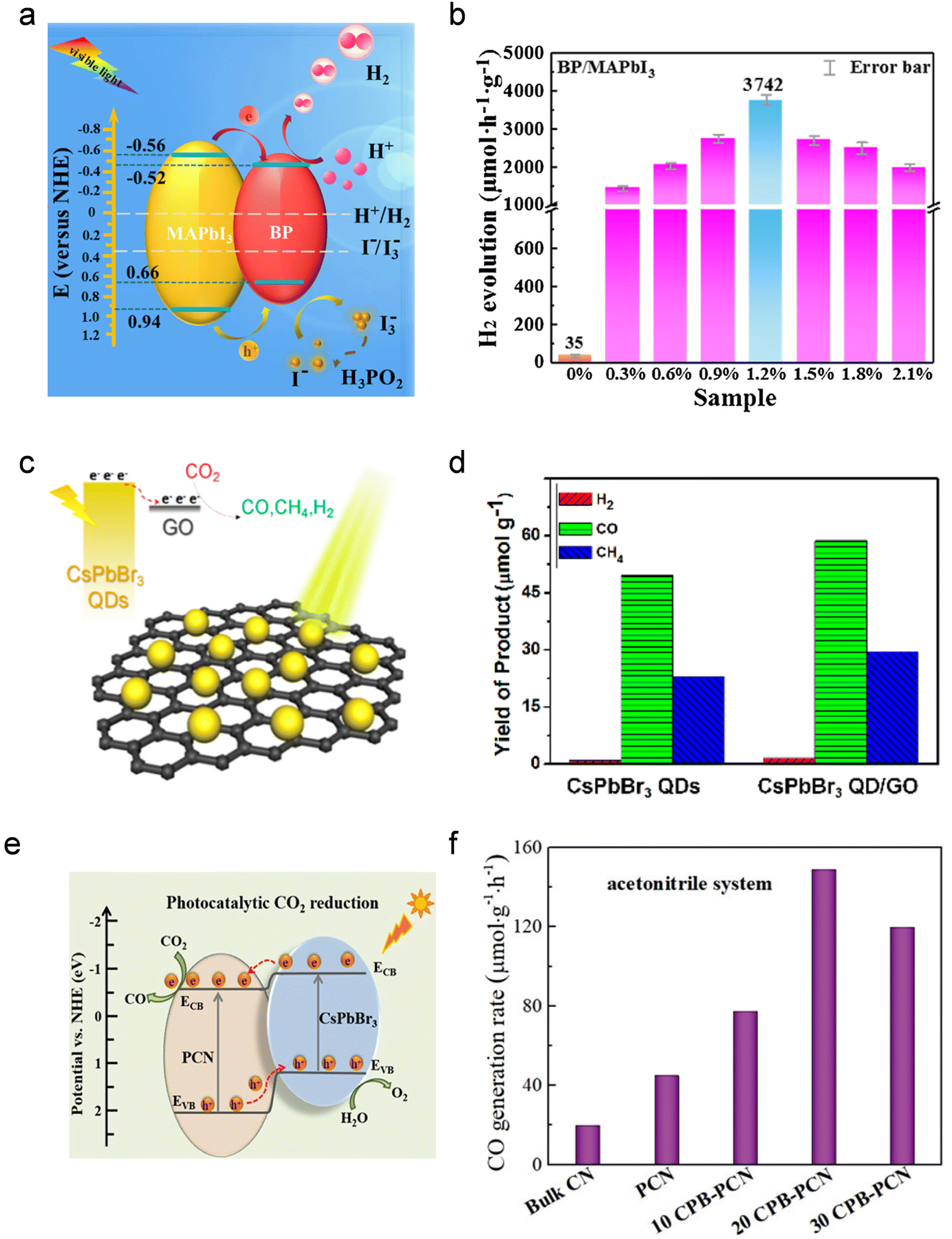 | ||
| Fig. 15 Photocatalytic mechanism and performance of HP/2D material interfaces considering the HER and CO2 reduction. (a) Schematic illustration of photogenerated charge transfer across the MAPbI3/BP interface under visible light (λ ≥ 420 nm) illumination. (b) Photocatalytic HER rates of MAPbI3/BP with different BP contents. Reproduced from ref. 262. Copyright 2019 Elsevier Ltd. (c) Schematic diagram of CO2 reduction at the CsPbBr3/GO interface. (d) Comparison of yield of CO2 reduction products after 12 h of photochemical reaction without and with GO. Reproduced from ref. 172. Copyright 2017 American Chemical Society. (e) Schematic illustration of CO2 reduction at the CsPbBr3/g-C3N4 interface. (f) Yield of CO in the acetonitrile/water system with different g-C3N4 contents. Reproduced from ref. 176. Copyright 2018 Wiley-VCH Verlag GmbH & Co. KGaA, Weinheim. | ||
In addition to the use of tunable bandgap 2D materials, mixed halogen HPs can be employed in photocatalytic applications. The CsPbBrCl2/g-C3N4 interface was employed to degrade complex anionic dyes.360 O2 does not spontaneously transform into the active radical ˙O2− as the redox potential of O2/˙O2− is lower than the CB edge of g-C3N4; similar obstacles exist for the OH−/˙OH and H2O/˙OH reactions at the VB edge of CsPbBrCl2. The unmatched band gap hinders the effective decomposition of Eosin B. The formation of the CsPbBrCl2/g-C3N4 interface facilitates the photocatalytic degradation of toxic Eosin B dye into non-toxic products, which generates an initiative electron and hole transfer process. A lead-free double perovskite Cs2AgBiBr6/RGO interface was applied to the HER in a saturated HBr aqueous solution. A high yield of 489 μmol h−1 g−1 was obtained under visible light irradiation for over 10 h and the continuous photocatalytic HER was achieved with an excellent stability of over 120 h. The superior photocatalytic performance can be attributed to the accumulated transfer of electrons from Cs2AgBiBr6 to RGO through M–O–C bonds. The HER activity and stability of MAPbBr3/RGO were studied further. Compared with pure MAPbBr3 and MAPbBr3/Pt, MAPbBr3/RGO elevated the HER activity significantly (approximately 67 times). The activity did not exhibit any noticeable decline after 20 experimental cycles. Thickness-dependent WS2 nanosheets were coupled with γ-CsPbI3 to explore their photocatalytic properties.173 It was observed that few-layered WS2 nanosheets exhibit better photocatalytic performance with superior charge transfer, generating sufficient hydroxyl radicals for the degradation of methylene blue (MB).
5. Conclusions and prospects
Herein, we provide a timely and comprehensive review on the construction of HP/2D material interfaces, summarizing the recent advances with an emphasis on the interfacial properties and relevant applications. Insights into the synthetic strategies, interfacial properties and applications of HP/2D material interfaces will trigger new possibilities to create novel interfaces, architectures and devices, leading to the conceptual development of related domains. Although significant achievements have been made in the development of HPs and 2D materials, HP/2D material interfaces are still in the initial research stages and are far from practical application. Consequently, we propose several research directions for HP/2D material interfaces, which could provide guidance for future development in this field.The development of new HPs and 2D materials is a considerable challenge. The bandgap tunability of HPs can be used to generate emissions across the entire visible spectrum, and their soft crystal structure makes them suitable for component substitution, to achieve unprecedented characteristics. Previous studies have revealed that the incorporation of larger organic A cations induces a high distortion level in the inorganic structures of HPs, resulting in broadband white-light emission. This is because the highly distorted B–X framework promotes the generation of additional transient photoexcited STE states resulting from strong electron−phonon coupling.361 Notably, studies on NIR emission from HPs are of great importance and worthy of more attention. NIR emission is a vital part of the lighting field and has several applications in food detection, plant lighting and thermal imaging. As typical phosphors suffer from low efficiency and a narrow peak width, HPs with NIR emission could better satisfy practical demands. In reality, NIR emission LEDs based on iodine-containing HPs have been achieved with promising EQEs.287,351,362,363 We believe that chemical doping or structural distortion may further help regulate the NIR emission from HPs. Recently, some studies have been conducted on Cr3+ doping in phosphors, which could also be applied to HPs for achieving NIR emission. Controlling structural distortion in HPs might also help achieve NIR emission. Although the correlation between STE states and white-light emission is unclear, structural distortions generally correspond to trap levels. Theoretically, deeper trap levels could be realized by adjusting the structural distortions of matched HPs, thereby spontaneously transferring the bandgaps of HPs from the visible region to the NIR region. In addition, there is an urgent need to develop lead-free HPs. The toxicity of lead is a grave threat to the human body and the environment, which severely hinders the large-scale application of lead-containing HPs. Moreover, new 2D materials, such as phosphorene, silicene and germanene, should be developed and combined with HPs to form interfaces for various applications owing to their different properties.
The design ideas of HP/2D material interfaces and their corresponding interfacial properties should be studied systematically. The interface plays a crucial role in carrier recombination and charge separation and transfer between HPs and 2D materials, which in turn affects the device performance. However, it is a challenge to construct a desired HP/2D material interface due to the lack of theoretical guidance on the connection between interfacial properties and device fabrication protocols. To realize suitable optoelectronic devices, the potential barrier at the interface, which is determined by the potential differences between HPs and 2D materials, should be considered carefully. The combination mode of the interface is important as well. As discussed in Section 3.1, the preparation of HP/2D material interfaces is closely related to their interfacial behavior. The interfaces of low-dimensional HPs/2D materials are formed by lattice mismatching or bonding anchoring, whereas weak van der Waals forces are used to form high-dimensional HP/2D material hybrid structures. Understanding the formation of HP/2D material interfaces can promote the development of interfacial modifications and various device designs. Furthermore, stacked designs of HPs and 2D materials should be explored. In recent years, research on the twist angle in bilayer 2D materials has increased significantly.364–367 The electronic band structure of ‘twisted bilayer graphene’ exhibits flat bands near zero Fermi energy, with twist angles of approximately 1.1°, resulting in correlated insulating states at half-filling. This suggests that the interfacial behavior of bilayer 2D materials is completely modified at a certain angle. HP/2D material interfaces are similar to bilayer 2D materials and some unexpected interfacial properties are yet be unearthed.
The stability of HP/2D material interfaces must be enhanced as it is a significant factor that hinders their practical application. High stability requires sufficient surface passivation which may in return degrade the performance as excessive surface passivation could affect the interfacial charge behavior of HPs. To this regard, a surface ligand with an appropriate carbon chain length is the key to maintain the balance between the stability and performance.368–370 The development of suitable packing technologies is a probable approach to solve this problem, but packing instruments are expensive and the related technology is complicated. Nevertheless, there is considerable belief that the intrinsic stability of HP/2D material interfaces can be improved. In our opinion, HPs can be embedded into a 2D material matrix to achieve a balance between stability and performance. The 2D material could serve as a protective layer without offsetting the charge behavior. However, this requires precise control over the construction of HP/2D material interfaces. The stepwise synthesis method could be adapted to design HP/2D material interfaces with excellent stability. The as-prepared HP grains would serve as crystal nuclei for the epitaxial growth of 2D materials, guaranteeing strong contact between the two materials and sufficient protection of the inner HPs. Although this idea does not consider the potential difficulties that may occur during the synthesis process, it could be a suitable avenue for overcoming the stability problems of HP/2D material interfaces.
Conflicts of interest
There are no conflicts to declare.Acknowledgements
This work was supported by the National Natural Science Foundation of China (Grant No. 52072349 and 52172162), the Natural Science Foundation of Zhejiang Province (LR22E020004), the Fundamental Research Funds for the Central Universities, China University of Geosciences (Wuhan) (No. 162301202610), the Natural Science Foundation of Guangdong Province (2022A1515012145) and Shenzhen Science and Technology Program (No. JCYJ20220530162403007). This work was performed in part at the Melbourne Center for Nanofabrication (MCN) in the Victorian Node of the Australian National Fabrication Facility (ANFF).Notes and references
- Y.-S. Park, S. Guo, N. S. Makarov and V. I. Klimov, ACS Nano, 2015, 9, 10386–10393 CrossRef CAS PubMed.
- J. Lin, Y. Lu, X. Li, F. Huang, C. Yang, M. Liu, N. Jiang and D. Chen, ACS Energy Lett., 2021, 6, 519–528 CrossRef CAS.
- H. Liu, Z. Wu, J. Shao, D. Yao, H. Gao, Y. Liu, W. Yu, H. Zhang and B. Yang, ACS Nano, 2017, 11, 2239–2247 CrossRef CAS.
- J. Liu, B. Shabbir, C. Wang, T. Wan, Q. Ou, P. Yu, A. Tadich, X. Jiao, D. Chu, D. Qi, D. Li, R. Kan, Y. Huang, Y. Dong, J. Jasieniak, Y. Zhang and Q. Bao, Adv. Mater., 2019, 31, e1901644 CrossRef PubMed.
- Y. Wang, X. Li, J. Song, L. Xiao, H. Zeng and H. Sun, Adv. Mater., 2015, 27, 7101–7108 CrossRef CAS PubMed.
- H. Huang, A. S. Susha, S. V. Kershaw, T. F. Hung and A. L. Rogach, Adv. Sci, 2015, 2, 1500194 CrossRef.
- K. Wu, G. Liang, Q. Shang, Y. Ren, D. Kong and T. Lian, J. Am. Chem. Soc., 2015, 137, 12792–12795 CrossRef CAS.
- A. Kojima, K. Teshima, Y. Shirai and T. Miyasaka, J. Am Chem. Soc., 2009, 131, 6050–6051 CrossRef CAS.
- Q. Jiang, Y. Zhao, X. Zhang, X. Yang, Y. Chen, Z. Chu, Q. Ye, X. Li, Z. Yin and J. You, Nat. Photon, 2019, 13, 460–466 CrossRef CAS.
- H. Min, D. Y. Lee, J. Kim, G. Kim, K. S. Lee, J. Kim, M. J. Paik, Y. K. Kim, K. S. Kim, M. G. Kim, T. J. Shin and S. Il Seok, Nature, 2021, 598, 444–450 CrossRef CAS PubMed.
- Z. Liu, W. Qiu, X. Peng, G. Sun, X. Liu, D. Liu, Z. Li, F. He, C. Shen, Q. Gu, F. Ma, H. L. Yip, L. Hou, Z. Qi and S. J. Su, Adv. Mater., 2021, 33, e2103268 CrossRef.
- F. Bella, Electrochim. Acta, 2015, 175, 151–161 CrossRef CAS.
- A. Abate, J. P. Correa-Baena, M. Saliba, M. S. Su'ait and F. Bella, Chem. – Eur. J, 2018, 24, 3083–3100 CrossRef CAS.
- F. Bella, P. Renzi, C. Cavallo and C. Gerbaldi, Chem. – Eur. J, 2018, 24, 12183–12205 CrossRef CAS.
- L. Fagiolari and F. Bella, Energy Environ. Sci., 2019, 12, 3437–3472 RSC.
- W.-J. Gao, J. Xia, J. Xiao, H.-J. Yu, D. Wang, A. Shinohara, C. Jia, D.-B. Kuang and G. Shao, Chem. Eng. J, 2022, 437, 135197 CrossRef CAS.
- S. Mattiello, G. Lucarelli, A. Calascibetta, L. Polastri, E. Ghiglietti, S. K. Podapangi, T. M. Brown, M. Sassi and L. Beverina, ACS Sustainable Chem. Eng, 2022, 10, 4750–4757 CrossRef CAS.
- E. Pulli, E. Rozzi and F. Bella, Energy Convers. Manage., 2020, 219, 112982 CrossRef.
- J. C. de Haro, E. Tatsi, L. Fagiolari, M. Bonomo, C. Barolo, S. Turri, F. Bella and G. Griffini, ACS Sustainable Chem. Eng, 2021, 9, 8550–8560 CrossRef CAS.
- T. M. W. J. Bandara, J. M. C. Hansadi and F. Bella, Ionics, 2022, 28, 2563–2583 CrossRef CAS.
- L. Fagiolari, M. Sampò, A. Lamberti, J. Amici, C. Francia, S. Bodoardo and F. Bella, Energy Storage Mater, 2022, 51, 400–434 CrossRef.
- J. A. Dawson, A. J. Naylor, C. Eames, M. Roberts, W. Zhang, H. J. Snaith, P. G. Bruce and M. S. Islam, ACS Energy Lett, 2017, 2, 1818–1824 CrossRef CAS.
- N. Vicente, D. Bresser, S. Passerini and G. Garcia-Belmonte, ChemElectroChem, 2019, 6, 456–460 CrossRef CAS.
- Q. Wang, T. Yang, H. Wang, J. Zhang, X. Guo, Z. Yang, S. Lu and W. Qin, CrystEngComm, 2019, 21, 1048–1059 RSC.
- D. Ramirez, Y. Suto, N. C. Rosero-Navarro, A. Miura, K. Tadanaga and F. Jaramillo, Inorg. Chem., 2018, 57, 4181–4188 CrossRef CAS.
- N. Vicente and G. Garcia-Belmonte, J. Phys. Chem. Lett., 2017, 8, 1371–1374 CrossRef CAS.
- M. Tathavadekar, S. Krishnamurthy, A. Banerjee, S. Nagane, Y. Gawli, A. Suryawanshi, S. Bhat, D. Puthusseri, A. D. Mohite and S. Ogale, J. Mater. Chem. A, 2017, 5, 18634–18642 RSC.
- J. Wu, X. Li, Y. Zhao, L. Liu, W. Qu, R. Luo, R. Chen, Y. Li and Q. Chen, J. Mater. Chem. A, 2018, 6, 20896–20903 RSC.
- L. Zhang, J. Miao, J. Li and Q. Li, Adv. Funct. Mater., 2020, 30, 2003653 CrossRef CAS.
- F. Bella, G. Griffini, J.-P. Correa-Baena, G. Saracco, M. Grätzel, A. Hagfeldt, S. Turri and C. Gerbaldi, Science, 2016, 354, 203–206 CrossRef CAS.
- I. Popoola, M. Gondal, L. Oloore, A. Popoola and J. AlGhamdi, Electrochim. Acta, 2020, 332, 135536 CrossRef CAS.
- J. A. Sichert, Y. Tong, N. Mutz, M. Vollmer, S. Fischer, K. Z. Milowska, R. Garcia Cortadella, B. Nickel, C. Cardenas-Daw, J. K. Stolarczyk, A. S. Urban and J. Feldmann, Nano Lett, 2015, 15, 6521–6527 CrossRef CAS PubMed.
- G. Li, H. Wang, T. Zhang, L. Mi, Y. Zhang, Z. Zhang, W. Zhang and Y. Jiang, Adv. Funct. Mater., 2016, 26, 8478–8486 CrossRef CAS.
- J. Song, J. Li, X. Li, L. Xu, Y. Dong and H. Zeng, Adv. Mater., 2015, 27, 7162–7167 CrossRef CAS PubMed.
- L. J. Chen, C. R. Lee, Y. J. Chuang, Z. H. Wu and C. Chen, J. Phys. Chem. Lett., 2016, 7, 5028–5035 CrossRef CAS PubMed.
- V. A. Hintermayr, A. F. Richter, F. Ehrat, M. Doblinger, W. Vanderlinden, J. A. Sichert, Y. Tong, L. Polavarapu, J. Feldmann and A. S. Urban, Adv. Mater., 2016, 28, 9478–9485 CrossRef CAS.
- I. Rosa-Pardo, M. Rando-Brotons, S. Pocoví-Martínez, R. E. Galian and J. Pérez Prieto, ChemNanoMat, 2019, 5, 328–333 CrossRef CAS.
- H. Liu, Z. Wu, H. Gao, J. Shao, H. Zou, D. Yao, Y. Liu, H. Zhang and B. Yang, ACS Appl. Mater. Interfaces, 2017, 9, 42919–42927 CrossRef CAS.
- A. Kostopoulou, K. Brintakis, N. K. Nasikas and E. Stratakis, Nanophotonics, 2019, 8, 1607–1640 CAS.
- A. Kostopoulou, E. Kymakis and E. Stratakis, J. Mater. Chem. A, 2018, 6, 9765–9798 RSC.
- H.-R. Xia, W.-T. Sun and L.-M. Peng, Chem Commun, 2015, 51, 13787–13790 RSC.
- A. Kostopoulou, D. Vernardou, K. Savva and E. Stratakis, Nanoscale, 2019, 11, 882–889 RSC.
- H. Kong, J. Wu, Y. Han, Y. Zhang, N. Zhou, Q. Chen, W. Sun, H. Zhou and L.-M. Peng, J. Energy Chem, 2022, 72, 73–80 CrossRef CAS.
- S. Hou, Y. Guo, Y. Tang and Q. Quan, ACS Appl. Mater. Interfaces, 2017, 9, 18417–18422 CrossRef CAS.
- B. A. Nejand, V. Ahmadi, S. Gharibzadeh and H. R. Shahverdi, ChemSusChem, 2016, 9, 302–313 CrossRef CAS PubMed.
- C. Lu, I. T. Choi, J. Kim and H. K. Kim, J. Mater. Chem. A, 2017, 5, 20263–20276 RSC.
- M. L. Petrus, T. Bein, T. J. Dingemans and P. Docampo, J. Mater. Chem. A, 2015, 3, 12159–12162 RSC.
- S. Sajid, A. M. Elseman, H. Huang, J. Ji, S. Dou, H. Jiang, X. Liu, D. Wei, P. Cui and M. Li, Nano Energy, 2018, 51, 408–424 CrossRef CAS.
- Y. Liu, Z. Yang, D. Cui, X. Ren, J. Sun, X. Liu, J. Zhang, Q. Wei, H. Fan, F. Yu, X. Zhang, C. Zhao and S. F. Liu, Adv. Mater., 2015, 27, 5176–5183 CrossRef CAS PubMed.
- S. D. Stranks, R. L. Z. Hoye, D. Di, R. H. Friend and F. Deschler, Adv. Mater., 2019, 31, e1803336 CrossRef.
- Y. Hu, Y. Chu, Q. Wang, Z. Zhang, Y. Ming, A. Mei, Y. Rong and H. Han, Joule, 2019, 3, 2076–2085 CrossRef CAS.
- L. Meng, J. You and Y. Yang, Nat. Commun., 2018, 9, 5265 CrossRef CAS.
- C. Qin, A. S. D. Sandanayaka, C. Zhao, T. Matsushima, D. Zhang, T. Fujihara and C. Adachi, Nature, 2020, 585, 53–57 CrossRef CAS.
- S. G. Benka, Phys. Today, 2005, 58, 9 Search PubMed.
- K. S. Novoselov, V. I. Fal'ko, L. Colombo, P. R. Gellert, M. G. Schwab and K. Kim, Nature, 2012, 490, 192–200 CrossRef CAS.
- K. Novoselov and A. K. SGeim, Nature, 2007, 6, 183–191 CrossRef.
- K. Kim, J. Y. Choi, T. Kim, S. H. Cho and H. J. Chung, Nature, 2011, 479, 338–344 CrossRef CAS PubMed.
- A. K. Geim and I. V. Grigorieva, Nature, 2013, 499, 419–425 CrossRef CAS PubMed.
- K. Khan, A. K. Tareen, M. Aslam, R. Wang, Y. Zhang, A. Mahmood, Z. Ouyang, H. Zhang and Z. Guo, J. Mater. Chem. C, 2020, 8, 387–440 RSC.
- C. Tan, X. Cao, X. J. Wu, Q. He, J. Yang, X. Zhang, J. Chen, W. Zhao, S. Han, G. H. Nam, M. Sindoro and H. Zhang, Chem. Rev., 2017, 117, 6225–6331 CrossRef CAS PubMed.
- K. S. Novoselov, A. K. Geim, S. V. Morozov, D. Jiang, Y. Zhang, S. V. Dubonos, I. V. Grigorieva and A. A. Firsov, Science, 2004, 306, 666–669 CrossRef CAS PubMed.
- A. K. Geim and K. S. Novoselov, Nat. Mater., 2007, 6, 183 CrossRef CAS PubMed.
- J. Wang, F. Ma, W. Liang and M. Sun, Mater. Today Phys., 2017, 2, 6–34 CrossRef.
- X. Chen, H. Yang, B. Wu, L. Wang, Q. Fu and Y. Liu, Adv. Mater., 2019, 31, e1805582 CrossRef PubMed.
- J. Kim, S. S. Baik, S. H. Ryu, Y. Sohn, S. Park, B.-G. Park, J. Denlinger, Y. Yi, H. J. Choi and K. S. Kim, Science, 2015, 349, 723–726 CrossRef CAS PubMed.
- M. Chhowalla, Z. Liu and H. Zhang, Chem. Soc. Rev., 2015, 44, 2584–2586 RSC.
- S. Susarla, A. Kutana, J. A. Hachtel, V. Kochat, A. Apte, R. Vajtai, J. C. Idrobo, B. I. Yakobson, C. S. Tiwary and P. M. Ajayan, Adv. Mater., 2017, 29, 1702457 CrossRef.
- C. Li, Q. Cao, F. Wang, Y. Xiao, Y. Li, J. J. Delaunay and H. Zhu, Chem. Soc. Rev., 2018, 47, 4981–5037 RSC.
- Y. Li, H. Shao, Z. Lin, J. Lu, L. Liu, B. Duployer, P. O. A. Persson, P. Eklund, L. Hultman, M. Li, K. Chen, X. H. Zha, S. Du, P. Rozier, Z. Chai, E. Raymundo-Pinero, P. L. Taberna, P. Simon and Q. Huang, Nat. Mater., 2020, 19, 894–899 CrossRef CAS.
- P. Simon and Y. Gogotsi, Nat. Mater., 2020, 19, 1151–1163 CrossRef CAS PubMed.
- K. P. Bera, G. Haider, Y. T. Huang, P. K. Roy, C. R. Paul Inbaraj, Y. M. Liao, H. I. Lin, C. H. Lu, C. Shen, W. Y. Shih, W. H. Shih and Y. F. Chen, ACS Nano, 2019, 13, 12540–12552 CrossRef CAS.
- G. Kakavelakis, T. Maksudov, D. Konios, I. Paradisanos, G. Kioseoglou, E. Stratakis and E. Kymakis, Adv. Energy Mater, 2017, 7, 1602120 CrossRef.
- M. Hadadian, J. P. Correa-Baena, E. K. Goharshadi, A. Ummadisingu, J. Y. Seo, J. Luo, S. Gholipour, S. M. Zakeeruddin, M. Saliba, A. Abate, M. Gratzel and A. Hagfeldt, Adv. Mater., 2016, 28, 8681–8686 CrossRef CAS PubMed.
- Q. A. Akkerman, V. D'Innocenzo, S. Accornero, A. Scarpellini, A. Petrozza, M. Prato and L. Manna, J. Am. Chem. Soc., 2015, 137, 10276–10281 CrossRef CAS PubMed.
- L. Protesescu, S. Yakunin, M. I. Bodnarchuk, F. Krieg, R. Caputo, C. H. Hendon, R. X. Yang, A. Walsh and M. V. Kovalenko, Nano Lett, 2015, 15, 3692–3696 CrossRef CAS PubMed.
- J. Liang, Q. Fang, H. Wang, R. Xu, S. Jia, Y. Guan, Q. Ai, G. Gao, H. Guo, K. Shen, X. Wen, T. Terlier, G. P. Wiederrecht, X. Qian, H. Zhu and J. Lou, Adv. Mater., 2020, 32, e2004111 CrossRef.
- M. I. Saidaminov, J. Almutlaq, S. Sarmah, I. Dursun, A. A. Zhumekenov, R. Begum, J. Pan, N. Cho, O. F. Mohammed and O. M. Bakr, ACS Energy Lett, 2016, 1, 840–845 CrossRef CAS.
- B. Saparov, F. Hong, J.-P. Sun, H.-S. Duan, W. Meng, S. Cameron, I. G. Hill, Y. Yan and D. B. Mitzi, Chem. Mater., 2015, 27, 5622–5632 CrossRef CAS.
- A. Wang, X. Yan, M. Zhang, S. Sun, M. Yang, W. Shen, X. Pan, P. Wang and Z. Deng, Chem. Mater., 2016, 28, 8132–8140 CrossRef CAS.
- M. Xia, J. H. Yuan, G. Niu, X. Du, L. Yin, W. Pan, J. Luo, Z. Li, H. Zhao, K. H. Xue, X. Miao and J. Tang, Adv. Funct. Mater., 2020, 30, 1910648 CrossRef CAS.
- Z. Xiao, Z. Song and Y. Yan, Adv. Mater., 2019, 31, e1803792 CrossRef PubMed.
- W. Zhang, K. Tao, C. Ji, Z. Sun, S. Han, J. Zhang, Z. Wu and J. Luo, Inorg. Chem., 2018, 57, 4239–4243 CrossRef CAS.
- W. Pan, H. Wu, J. Luo, Z. Deng, C. Ge, C. Chen, X. Jiang, W.-J. Yin, G. Niu, L. Zhu, L. Yin, Y. Zhou, Q. Xie, X. Ke, M. Sui and J. Tang, Nat. Photon, 2017, 11, 726–732 CrossRef CAS.
- R. Yang, R. Li, Y. Cao, Y. Wei, Y. Miao, W. L. Tan, X. Jiao, H. Chen, L. Zhang, Q. Chen, H. Zhang, W. Zou, Y. Wang, M. Yang, C. Yi, N. Wang, F. Gao, C. R. McNeill, T. Qin, J. Wang and W. Huang, Adv. Mater., 2018, 30, e1804771 CrossRef.
- B. M. Benin, D. N. Dirin, V. Morad, M. Wçrle, S. Yakunin, G. Rainm, O. Nazarenko, M. Fischer, I. Infante and M. V. Kovalenko, Angew. Chem., Int. Ed, 2018, 57, 11329–11333 CrossRef CAS.
- M.-H. Du, ACS Energy Lett, 2020, 5, 464–469 CrossRef CAS.
- R. Gautier, F. Massuyeau, G. Galnon and M. Paris, Adv. Mater., 2019, 31, e1807383 CrossRef.
- X. Liu, X. Xu, B. Li, L. Yang, Q. Li, H. Jiang and D. Xu, Small, 2020, 16, e2002547 CrossRef.
- J. Yu, J. Kong, W. Hao, X. Guo, H. He, W. R. Leow, Z. Liu, P. Cai, G. Qian, S. Li, X. Chen and X. Chen, Adv. Mater., 2019, 31, e1806385 Search PubMed.
- R. Zeng, L. Zhang, Y. Xue, B. Ke, Z. Zhao, D. Huang, Q. Wei, W. Zhou and B. Zou, J. Phys. Chem. Lett., 2020, 11, 2053–2061 CrossRef CAS PubMed.
- Z. G. Dai, X. H. Xiao, W. Wu, Y. P. Zhang, L. Liao, S. S. Guo, J. J. Ying, C. X. Shan, M. T. Sun and C. Z. Jiang, Light: Sci. Appl., 2015, 4, e342–e342 CrossRef CAS.
- X. Zhang, Z. Dai, S. Si, X. Zhang, W. Wu, H. Deng, F. Wang, X. Xiao and C. Jiang, Small, 2017, 13, 1603347 CrossRef.
- V. Chandra and K. S. Kim, Chem. Commun., 2011, 47, 3942–3944 RSC.
- S. Xi, L. Wang, H. Xie and W. Yu, ACS Nano, 2022, 16, 3843–3851 CrossRef CAS PubMed.
- Y. Lu, X. L. Liu, L. He, Y. X. Zhang, Z. Y. Hu, G. Tian, X. Cheng, S. M. Wu, Y. Z. Li, X. H. Yang, L. Y. Wang, J. W. Liu, C. Janiak, G. G. Chang, W. H. Li, G. Van Tendeloo, X. Y. Yang and B. L. Su, Nano Lett, 2020, 20, 3122–3129 CrossRef CAS PubMed.
- D. Jariwala, V. K. Sangwan, L. J. Lauhon, T. J. Marks and M. C. Hersam, ACS Nano, 2014, 8, 1102–1120 CrossRef CAS PubMed.
- H. Wang, H. Yuan, S. Sae Hong, Y. Li and Y. Cui, Chem. Soc. Rev., 2015, 44, 2664–2680 RSC.
- J. Kim, S. Byun, A. J. Smith, J. Yu and J. Huang, J. Phys. Chem. Lett., 2013, 4, 1227–1232 CrossRef CAS PubMed.
- Q. H. Wang, K. Kalantar-Zadeh, A. Kis, J. N. Coleman and M. S. Strano, Nat. Nanotech, 2012, 7, 699–712 CrossRef CAS.
- K. F. Mak and J. Shan, Nat. Photon, 2016, 10, 216–226 CrossRef CAS.
- H. Guo, N. Lu, L. Wang, X. Wu and X. C. Zeng, J. Phys. Chem. C, 2014, 118, 7242–7249 CrossRef CAS.
- B. Ouyang, Z. Mi and J. Song, J. Phys. Chem. C, 2016, 120, 8927–8935 CrossRef CAS.
- J. You, Z. Hong, Y. M. Yang, Q. Chen, M. Cai, T.-B. Song, C.-C. Chen, S. Lu, Y. Liu, H. Zhou and Y. Yang, ACS Nano, 2014, 8, 1674–1680 CrossRef CAS PubMed.
- Y. Luo, S. Aharon, M. Stuckelberger, E. Magaña, B. Lai, M. I. Bertoni, L. Etgar and D. P. Fenning, Adv. Funct. Mater., 2018, 28, 1706995 CrossRef.
- W. Chen, Y. Shi, J. Chen, P. Ma, Z. Fang, D. Ye, Y. Lu, Y. Yuan, J. Zhao and Z. Xiao, Adv. Mater., 2021, 33, e2104842 CrossRef PubMed.
- M. Fahim, I. Firdous, S.-W. Tsang and W. A. Daoud, Nano Energy, 2022, 96, 107058 CrossRef CAS.
- E. Han, J. Yu, E. Annevelink, J. Son, D. A. Kang, K. Watanabe, T. Taniguchi, E. Ertekin, P. Y. Huang and A. M. van der Zande, Nat. Mater., 2020, 19, 305–309 CrossRef CAS PubMed.
- X. Li, D. Yu, J. Chen, Y. Wang, F. Cao, Y. Wei, Y. Wu, L. Wang, Y. Zhu, Z. Sun, J. Ji, Y. Shen, H. Sun and H. Zeng, ACS Nano, 2017, 11, 2015–2023 CrossRef CAS PubMed.
- Q. Tu, I. Spanopoulos, P. Yasaei, C. C. Stoumpos, M. G. Kanatzidis, G. S. Shekhawat and V. P. Dravid, ACS Nano, 2018, 12, 10347–10354 CrossRef CAS PubMed.
- S. Das, D. Pandey, J. Thomas and T. Roy, Adv. Mater., 2019, 31, e1802722 CrossRef PubMed.
- J. Du, H. Yu, B. Liu, M. Hong, Q. Liao, Z. Zhang and Y. Zhang, Small Methods, 2021, 5, e2000919 CrossRef PubMed.
- Z. Lin, Z. Wan, F. Song, B. Huang, C. Jia, Q. Qian, J. S. Kang, Y. Wu, X. Yan, L. Peng, C. Wan, J. Zhou, Z. Sofer, I. Shakir, Z. Almutairi, S. Tolbert, X. Pan, Y. Hu, Y. Huang and X. Duan, Chemistry, 2021, 7, 1887–1902 CrossRef CAS.
- B. Zhao, Z. Wan, Y. Liu, J. Xu, X. Yang, D. Shen, Z. Zhang, C. Guo, Q. Qian, J. Li, R. Wu, Z. Lin, X. Yan, B. Li, Z. Zhang, H. Ma, B. Li, X. Chen, Y. Qiao, I. Shakir, Z. Almutairi, F. Wei, Y. Zhang, X. Pan, Y. Huang, Y. Ping, X. Duan and X. Duan, Nature, 2021, 591, 385–390 CrossRef CAS PubMed.
- Z. Yan, D. Xu, Z. Lin, P. Wang, B. Cao, H. Ren, F. Song, C. Wan, L. Wang, J. Zhou, X. Zhao, J. Chen, Y. Huang and X. Duan, Science, 2022, 375, 852–859 CrossRef CAS PubMed.
- S. Yu, X. Wu, Y. Wang, X. Guo and L. Tong, Adv. Mater., 2017, 29, 1606128 CrossRef.
- N. R. Glavin, R. Rao, V. Varshney, E. Bianco, A. Apte, A. Roy, E. Ringe and P. M. Ajayan, Adv. Mater., 2020, 32, e1904302 CrossRef.
- X. Zhang, L. Hou, A. Ciesielski and P. Samorì, Adv. Energy. Mater, 2016, 6, 1600671 CrossRef.
- X. Cai, Y. Luo, B. Liu and H. M. Cheng, Chem. Soc. Rev., 2018, 47, 6224–6266 RSC.
- L. Shi and T. Zhao, J. Mater. Chem. A, 2017, 5, 3735–3758 RSC.
- P. Chen, T. L. Atallah, Z. Lin, P. Wang, S. J. Lee, J. Xu, Z. Huang, X. Duan, Y. Ping, Y. Huang, J. R. Caram and X. Duan, Nature, 2021, 599, 404–410 CrossRef CAS.
- T. Takagahara and K. Takeda, Phys. Rev. B: Condens. Matter, 1992, 46, 15578–15581 CrossRef CAS.
- H. Sung, N. Ahn, M. S. Jang, J.-K. Lee, H. Yoon, N.-G. Park and M. Choi, Adv. Energy Mater, 2016, 6, 1501873 CrossRef.
- L.-L. Jiang, Z.-K. Wang, M. Li, C.-C. Zhang, Q.-Q. Ye, K.-H. Hu, D.-Z. Lu, P.-F. Fang and L.-S. Liao, Adv. Funct. Mater., 2018, 28, 1705875 CrossRef.
- L. Najafi, B. Taheri, B. Martin-Garcia, S. Bellani, D. Di Girolamo, A. Agresti, R. Oropesa-Nunez, S. Pescetelli, L. Vesce, E. Calabro, M. Prato, A. E. Del Rio Castillo, A. Di Carlo and F. Bonaccorso, ACS Nano, 2018, 12, 10736–10754 CrossRef CAS.
- H. Chen, X.-L. Zhang, Y.-Y. Zhang, D. Wang, D.-L. Bao, Y. Que, W. Xiao, S. Du, M. Ouyang, S. T. Pantelides and H.-J. Gao, Science, 2019, 365, 1036–1040 CrossRef CAS.
- Y. Jiang, L. Qiu, E. J. Juarez-Perez, L. K. Ono, Z. Hu, Z. Liu, Z. Wu, L. Meng, Q. Wang and Y. Qi, Nat. Energy, 2019, 4, 585–593 CrossRef CAS.
- J. Jiang, X. Zou, Y. Lv, Y. Liu, W. Xu, Q. Tao, Y. Chai and L. Liao, Nat. Commun., 2020, 11, 4266 CrossRef CAS.
- K. Leng, L. Wang, Y. Shao, I. Abdelwahab, G. Grinblat, I. Verzhbitskiy, R. Li, Y. Cai, X. Chi, W. Fu, P. Song, A. Rusydi, G. Eda, S. A. Maier and K. P. Loh, Nat. Commun., 2020, 11, 5483 CrossRef CAS PubMed.
- K. Leng, I. Abdelwahab, I. Verzhbitskiy, M. Telychko, L. Chu, W. Fu, X. Chi, N. Guo, Z. Chen, Z. Chen, C. Zhang, Q. H. Xu, J. Lu, M. Chhowalla, G. Eda and K. P. Loh, Nat. Mater., 2018, 17, 908–914 CrossRef CAS.
- M. L. Aubrey, A. Saldivar Valdes, M. R. Filip, B. A. Connor, K. P. Lindquist, J. B. Neaton and H. I. Karunadasa, Nature, 2021, 597, 355–359 CrossRef CAS PubMed.
- J. Zhou, Z. Lin, H. Ren, X. Duan, I. Shakir, Y. Huang and X. Duan, Adv. Mater., 2021, 33, e2004557 CrossRef.
- P. Wang, B. Wang, Y. Liu, L. Li, H. Zhao, Y. Chen, J. Li, S. F. Liu and K. Zhao, Angew. Chem., Int. Ed., 2020, 59, 23100–23106 CrossRef CAS.
- N. Rivera and I. Kaminer, Nat. Rev. Phys., 2020, 2, 538–561 CrossRef.
- J. Gao, S. C. Nguyen, N. D. Bronstein and A. P. Alivisatos, ACS Photonics, 2016, 3, 1217–1222 CrossRef CAS.
- W. Shi, X. Zhang, H. S. Chen, K. Matras-Postolek and P. Yang, J. Mater. Chem. C, 2021, 9, 5732–5739 RSC.
- R. Cheng, D. Li, H. Zhou, C. Wang, A. Yin, S. Jiang, Y. Liu, Y. Chen, Y. Huang and X. Duan, Nano Lett, 2014, 14, 5590–5597 CrossRef CAS.
- C. H. Lee, G. H. Lee, A. M. van der Zande, W. Chen, Y. Li, M. Han, X. Cui, G. Arefe, C. Nuckolls, T. F. Heinz, J. Guo, J. Hone and P. Kim, Nat. Nanotech, 2014, 9, 676–681 CrossRef CAS.
- J. Song, L. Xu, J. Li, J. Xue, Y. Dong, X. Li and H. Zeng, Adv. Mater., 2016, 28, 4861–4869 CrossRef CAS PubMed.
- X. Gao, X. Zhang, W. Yin, H. Wang, Y. Hu, Q. Zhang, Z. Shi, V. L. Colvin, W. W. Yu and Y. Zhang, Adv. Sci, 2019, 6, 1900941 CrossRef CAS PubMed.
- Q. Fan, G. V. Biesold-McGee, J. Ma, Q. Xu, S. Pan, J. Peng and Z. Lin, Angew. Chem., Int. Ed, 2020, 59, 1030–1046 CrossRef CAS.
- B. R. Sutherland and E. H. Sargent, Nat. Photon, 2016, 10, 295–302 CrossRef CAS.
- K. F. Mak, C. Lee, J. Hone, J. Shan and T. F. Heinz, Phys. Rev. Lett., 2010, 105, 136805 CrossRef.
- J. H. Kim, H. S. Lee, G. H. An, J. Lee, H. M. Oh, J. Choi and Y. H. Lee, ACS Nano, 2020, 14, 11985–11994 CrossRef CAS PubMed.
- X. Huang, X. Feng, L. Chen, L. Wang, W. C. Tan, L. Huang and K.-W. Ang, Nano Energy, 2019, 62, 667–673 CrossRef CAS.
- S. Zhang, Y. Zhong, F. Yang, Q. Cao, W. Du, J. Shi and X. Liu, Photonics Res., 2020, 8, A72 CrossRef CAS.
- D. H. Luong, H. S. Lee, G. Ghimire, J. Lee, H. Kim, S. J. Yun, G. H. An and Y. H. Lee, Small, 2018, 14, e1802949 CrossRef PubMed.
- S. Peng, Q. Wei, B. Wang, Z. Zhang, H. Yang, G. Pang, K. Wang, G. Xing, X. W. Sun and Z. Tang, Angew. Chem., Int. Ed., 2020, 59, 22156–22162 CrossRef CAS.
- L. Chen, O. Skibitzki, L. Pedesseau, A. Letoublon, J. Stervinou, R. Bernard, C. Levallois, R. Piron, M. Perrin, M. A. Schubert, A. Moreac, O. Durand, T. Schroeder, N. Bertru, J. Even, Y. Leger and C. Cornet, ACS Nano, 2020, 14, 13127–13136 CrossRef.
- L. Ni, U. Huynh, A. Cheminal, T. H. Thomas, R. Shivanna, T. F. Hinrichsen, S. Ahmad, A. Sadhanala and A. Rao, ACS Nano, 2017, 11, 10834–10843 CrossRef CAS.
- S. Xue, T. Zhang, C. Yi, S. Zhang, X. Jia, L. H. Santos, C. Fang, Y. Shi, X. Zhu and J. Guo, Phys. Rev. B: Condens. Matter, 2019, 100, 195409 CrossRef CAS.
- A. D. Wright, C. Verdi, R. L. Milot, G. E. Eperon, M. A. Perez-Osorio, H. J. Snaith, F. Giustino, M. B. Johnston and L. M. Herz, Nat. Commun., 2016, 7, 11755 CrossRef.
- N. Driza, S. Blanco-Canosa, M. Bakr, S. Soltan, M. Khalid, L. Mustafa, K. Kawashima, G. Christiani, H. U. Habermeier, G. Khaliullin, C. Ulrich, M. Le Tacon and B. Keimer, Nat. Mater., 2012, 11, 675–681 CrossRef CAS PubMed.
- Z. Wang, S. McKeown Walker, A. Tamai, Y. Wang, Z. Ristic, F. Y. Bruno, A. de la Torre, S. Ricco, N. C. Plumb, M. Shi, P. Hlawenka, J. Sanchez-Barriga, A. Varykhalov, T. K. Kim, M. Hoesch, P. D. King, W. Meevasana, U. Diebold, J. Mesot, B. Moritz, T. P. Devereaux, M. Radovic and F. Baumberger, Nat. Mater., 2016, 15, 835–839 CrossRef CAS.
- Z. Guo, X. Wu, T. Zhu, X. Zhu and L. Huang, ACS Nano, 2016, 10, 9992–9998 CrossRef CAS.
- J. Nishida, J. P. Breen, K. P. Lindquist, D. Umeyama, H. I. Karunadasa and M. D. Fayer, J. Am. Chem. Soc., 2018, 140, 9882–9890 CrossRef CAS PubMed.
- F. Thouin, D. A. Valverde-Chavez, C. Quarti, D. Cortecchia, I. Bargigia, D. Beljonne, A. Petrozza, C. Silva and A. R. Srimath Kandada, Nat. Mater., 2019, 18, 349–356 CrossRef CAS PubMed.
- R. Heitz, I. Mukhametzhanov, O. Stier, A. Madhukar and D. Bimberg, Phy. Rev. Lett, 1999, 83, 4654–4657 CrossRef CAS.
- I. Lucci, S. Charbonnier, L. Pedesseau, M. Vallet, L. Cerutti, J. B. Rodriguez, E. Tournié, R. Bernard, A. Létoublon, N. Bertru, A. Le Corre, S. Rennesson, F. Semond, G. Patriarche, L. Largeau, P. Turban, A. Ponchet and C. Cornet, Phy. Rev. Mater, 2018, 2, 060401 CrossRef CAS.
- Z. Liu, J. Yang, J. Du, Z. Hu, T. Shi, Z. Zhang, Y. Liu, X. Tang, Y. Leng and R. Li, ACS Nano, 2018, 12, 5923–5931 CrossRef CAS.
- L. Wang, Y. Xue, M. Cui, Y. Huang, H. Xu, C. Qin, J. Yang, H. Dai and M. Yuan, Angew. Chem., Int. Ed., 2020, 59, 6442–6450 CrossRef CAS.
- X. Wang, Y. Wang, T. Zhang, X. Liu and Y. Zhao, Angew. Chem., Int. Ed., 2020, 59, 1469–1473 CrossRef CAS.
- M. Gramlich, B. J. Bohn, Y. Tong, L. Polavarapu, J. Feldmann and A. S. Urban, J. Phys. Chem. Lett., 2020, 11, 5361–5366 CrossRef CAS PubMed.
- J.-F. Liao, H.-S. Rao, B.-X. Chen, D.-B. Kuang and C.-Y. Su, J. Mater. Chem. A, 2017, 5, 2066–2072 RSC.
- S. Pan, Y. Chen, Z. Wang, Y.-W. Harn, J. Yu, A. Wang, M. J. Smith, Z. Li, V. V. Tsukruk, J. Peng and Z. Lin, Nano Energy, 2020, 77, 105043 CrossRef CAS.
- D. Yang, Y. Zou, P. Li, Q. Liu, L. Wu, H. Hu, Y. Xu, B. Sun, Q. Zhang and S.-T. Lee, Nano Energy, 2018, 47, 235–242 CrossRef CAS.
- H. C. Cheng, G. Wang, D. Li, Q. He, A. Yin, Y. Liu, H. Wu, M. Ding, Y. Huang and X. Duan, Nano Lett, 2016, 16, 367–373 CrossRef CAS PubMed.
- Z. Zhang, F. Sun, Z. Zhu, J. Dai, K. Gao, Q. Wei, X. Shi, Q. Sun, Y. Yan, H. Li, H. Yu, G. Xing, X. Huang and W. Huang, Sci. China Mater., 2018, 62, 43–53 CrossRef.
- B. Pradhan, S. Das, J. Li, F. Chowdhury, J. Cherusseri, D. Pandey, D. Dev, A. Krishnaprasad, E. Barrios, A. Towers, A. Gesquiere, L. Tetard, T. Roy and J. Thomas, Sci. Adv., 2020, 6, 5225 CrossRef.
- K. Chen, Y. Wang, J. Liu, J. Kang, Y. Ge, W. Huang, Z. Lin, Z. Guo, Y. Zhang and H. Zhang, Nanoscale, 2019, 11, 16852–16859 RSC.
- H. Huang, J. Li, Y. Yi, J. Wang, Y. Kang, P. K. Chu, H. C. Ong and X. F. Yu, Chem. Commun., 2018, 54, 2365–2368 RSC.
- Q. Wang, L. Tao, X. Jiang, M. Wang and Y. Shen, Appl. Surf. Sci., 2019, 465, 607–613 CrossRef CAS.
- Y. F. Xu, M. Z. Yang, B. X. Chen, X. D. Wang, H. Y. Chen, D. B. Kuang and C. Y. Su, J. Am. Chem. Soc., 2017, 139, 5660–5663 CrossRef CAS.
- Q. Zhang, M. Tai, Y. Zhou, Y. Zhou, Y. Wei, C. Tan, Z. Wu, J. Li and H. Lin, ACS Sustainable Chem. Eng, 2019, 8, 1219–1229 CrossRef.
- Q. Zhang, Y. Zhou, Y. Wei, M. Tai, H. Nan, Y. Gu, J. Han, X. Yin, J. Li and H. Lin, J. Mater. Chem. C, 2020, 8, 2569–2578 RSC.
- T. Wang, D. Yue, X. Li and Y. Zhao, Appl. Catal., B, 2020, 268, 118399 CrossRef CAS.
- M. Ou, W. Tu, S. Yin, W. Xing, S. Wu, H. Wang, S. Wan, Q. Zhong and R. Xu, Angew. Chem., Int. Ed, 2018, 57, 13570–13574 CrossRef CAS PubMed.
- L. Qiu, J. Hao, Y. Feng, X. Qu, G. Li, Y. Wei, G. Xing, H. Wang, C. Yan and J. Lin, J. Mater. Chem. C, 2019, 7, 4038–4042 RSC.
- A. Pan, M. J. Jurow, F. Qiu, J. Yang, B. Ren, J. J. Urban, L. He and Y. Liu, Nano Lett, 2017, 17, 6759–6765 CrossRef CAS PubMed.
- M. S. Hassan, P. Basera, S. Bera, M. Mittal, S. K. Ray, S. Bhattacharya and S. Sapra, ACS Appl. Mater. Interfaces, 2020, 12, 7317–7325 CrossRef CAS.
- Q. Zhang, H. Nan, Y. Zhou, Y. Gu, M. Tai, Y. Wei, F. Hao, J. Li, D. Oron and H. Lin, J. Mater. Chem. C, 2019, 7, 6795–6804 RSC.
- S. Muduli, P. Pandey, G. Devatha, R. Babar, M. Thripuranthaka, D. C. Kothari, M. Kabir, P. P. Pillai and S. Ogale, Angew. Chem., Int. Ed., 2018, 57, 7682–7686 CrossRef CAS.
- Y. Wu, P. Wang, X. Zhu, Q. Zhang, Z. Wang, Y. Liu, G. Zou, Y. Dai, M. H. Whangbo and B. Huang, Adv. Mater., 2018, 30, 1704342 CrossRef PubMed.
- S. Sun, D. Yuan, Y. Xu, A. Wang and Z. Deng, ACS Nano, 2016, 10, 3648–3657 CrossRef CAS PubMed.
- C. Zhang, J. Chen, L. Kong, L. Wang, S. Wang, W. Chen, R. Mao, L. Turyanska, G. Jia and X. Yang, Adv. Funct. Mater., 2021, 31, 2100438 CrossRef CAS.
- L. Zhang, S. Shen, M. Li, L. Li, J. Zhang, L. Fan, F. Cheng, C. Li, M. Zhu, Z. Kang, J. Su, T. Zhai and Y. Gao, Adv. Opt. Mater., 2019, 7, 1801744 CrossRef.
- C. K. Ng, H. Deng, H. Li, W. Yin, T. Alan and J. J. Jasieniak, J. Mater. Chem. C, 2021, 9, 313–321 RSC.
- A. Ishii and T. Miyasaka, Sci. Adv., 2020, 6, eabd3274 CrossRef CAS PubMed.
- J. Wu, X. Cong, S. Niu, F. Liu, H. Zhao, Z. Du, J. Ravichandran, P. H. Tan and H. Wang, Adv. Mater., 2019, 31, e1902118 CrossRef.
- G. Chen, Y. Qiu, H. Gao, Y. Zhao, J. Feng, L. Jiang and Y. Wu, Adv. Funct. Mater., 2020, 30, 1908894 CrossRef CAS.
- C. Wang, Y. Liu, X. Feng, C. Zhou, Y. Liu, X. Yu and G. Zhao, Angew. Chem., Int. Ed., 2019, 58, 11642–11646 CrossRef CAS PubMed.
- X. Xu, X. Zhang, W. Deng, J. Jie and X. Zhang, Small Methods, 2018, 2, 1700340 CrossRef.
- J.-H. Kim, Q. Van Le, T. P. Nguyen, T. H. Lee, H. W. Jang, W. S. Yun, S. M. Jeong, J. Lee, S. Y. Kim and H. Kim, Nano Energy, 2020, 70, 104497 CrossRef CAS.
- C. Zhang, K. Wang, N. Yi, Y. Gao, M. Zhu, W. Sun, S. Liu, K. Xu, S. Xiao and Q. Song, Adv. Opt. Mater., 2016, 4, 2057–2062 CrossRef CAS.
- Q. Xu, Z. Yang, D. Peng, J. Xi, P. Lin, Y. Cheng, K. Liu and C. Pan, Nano Energy, 2019, 65, 104001 CrossRef CAS.
- C. Fang, H. Wang, Z. Shen, H. Shen, S. Wang, J. Ma, J. Wang, H. Luo and D. Li, ACS Appl. Mater. Interfaces, 2019, 11, 8419–8427 CrossRef CAS PubMed.
- H. Yu, X. Cheng, Y. Wang, Y. Liu, K. Rong, Z. Li, Y. Wan, W. Gong, K. Watanabe, T. Taniguchi, S. Wang, J. Chen, Y. Ye and L. Dai, ACS Photonics, 2018, 5, 4520–4528 CrossRef CAS.
- Z. Wang, Q. Ou, Y. Zhang, Q. Zhang, H. Y. Hoh and Q. Bao, ACS Appl. Mater. Interfaces, 2018, 10, 24258–24265 CrossRef CAS.
- G.-H. Kim, H. Jang, Y. J. Yoon, J. Jeong, S. Y. Park, B. Walker, I.-Y. Jeon, Y. Jo, H. Yoon, M. Kim, J.-B. Baek, D. S. Kim and J. Y. Kim, Nano Lett, 2017, 17, 6385–6390 CrossRef CAS.
- H. Wu, H. Si, Z. Zhang, Z. Kang, P. Wu, L. Zhou, S. Zhang, Z. Zhang, Q. Liao and Y. Zhang, Adv. Sci, 2018, 5, 1801219 CrossRef.
- Q. A. Akkerman and L. Manna, ACS Energy Lett, 2020, 5, 604–610 CrossRef CAS PubMed.
- J. Young and J. M. Rondinelli, J. Phys. Chem. Lett., 2016, 7, 918–922 CrossRef CAS PubMed.
- M. Hu, C. Ge, J. Yu and J. Feng, J. Phys. Chem. C, 2017, 121, 27053–27058 CrossRef CAS.
- K. T. Butler, J. Mater. Chem. C, 2018, 6, 12045–12051 RSC.
- P. Wang, H. Xia, Q. Li, F. Wang, L. Zhang, T. Li, P. Martyniuk, A. Rogalski and W. Hu, Small, 2019, 15, e1904396 CrossRef.
- I. H. Abidi, L.-T. Weng, C. P. J. Wong, A. Tyagi, L. Gan, Y. Ding, M. Li, Z. Gao, R. Xue, M. D. Hossain, M. Zhuang, X. Ou and Z. Luo, Chem. Mater., 2018, 30, 1718–1728 CrossRef CAS.
- Y. Gao, S. Kim, S. Zhou, H. C. Chiu, D. Nelias, C. Berger, W. de Heer, L. Polloni, R. Sordan, A. Bongiorno and E. Riedo, Nat. Mater., 2015, 14, 714–720 CrossRef CAS PubMed.
- C. Zhang, S. Wang, H. Zhang, Y. Feng, W. Tian, Y. Yan, J. Bian, Y. Wang, S. Jin, S. M. Zakeeruddin, M. Grätzel and Y. Shi, Energy Environ. Sci., 2019, 12, 3585–3594 RSC.
- X. Wen, J. Wu, D. Gao and C. Lin, J. Mater. Chem. A, 2016, 4, 13482–13487 Search PubMed.
- A. L. Palma, L. Cinà, S. Pescetelli, A. Agresti, M. Raggio, R. Paolesse, F. Bonaccorso and A. Di Carlo, Nano Energy, 2016, 22, 349–360 CrossRef CAS.
- X. Zhao, L. Tao, H. Li, W. Huang, P. Sun, J. Liu, S. Liu, Q. Sun, Z. Cui, L. Sun, Y. Shen, Y. Yang and M. Wang, Nano Lett, 2018, 18, 2442–2449 CrossRef CAS PubMed.
- Y. Shao, Y. Liu, X. Chen, C. Chen, I. Sarpkaya, Z. Chen, Y. Fang, J. Kong, K. Watanabe, T. Taniguchi, A. Taylor, J. Huang and F. Xia, Nano Lett, 2017, 17, 7330–7338 CrossRef CAS PubMed.
- U. Dasgupta, S. Chatterjee and A. J. Pal, Sol. Energy Mater. Sol. Cells, 2017, 172, 353–360 CrossRef CAS.
- P. Wang, C. Jia, Y. Huang and X. Duan, Matter, 2021, 4, 552–581 CrossRef CAS.
- H. K. Seo, H. Kim, J. Lee, M. H. Park, S. H. Jeong, Y. H. Kim, S. J. Kwon, T. H. Han, S. Yoo and T. W. Lee, Adv. Mater., 2017, 29, 1605587 CrossRef.
- Y. Wang, Y. Zhou, T. Zhang, M.-G. Ju, L. Zhang, M. Kan, Y. Li, X. C. Zeng, N. P. Padture and Y. Zhao, Mater. Horiz., 2018, 5, 868–873 Search PubMed.
- J. M. Kim, C. W. Jang, J. H. Kim, S. Kim and S.-H. Choi, Appl. Surf. Sci., 2018, 455, 1131–1136 CrossRef CAS.
- J. H. Heo, D. H. Shin, S. Kim, M. H. Jang, M. H. Lee, S. W. Seo, S.-H. Choi and S. H. Im, Chem. Eng. J., 2017, 323, 153–159 Search PubMed.
- J. H. Heo, D. H. Shin, M. H. Jang, M. L. Lee, M. G. Kang and S. H. Im, J. Mater. Chem. A, 2017, 5, 21146–21152 RSC.
- S. Feng, Y. Yang, M. Li, J. Wang, Z. Cheng, J. Li, G. Ji, G. Yin, F. Song, Z. Wang, J. Li and X. Gao, ACS Appl. Mater. Interfaces, 2016, 8, 14503–14512 CrossRef CAS.
- A. Agresti, S. Pescetelli, L. Cinà, D. Konios, G. Kakavelakis, E. Kymakis and A. D. Carlo, Adv. Funct. Mater., 2016, 26, 2686–2694 Search PubMed.
- J. H. Heo, D. H. Shin, D. H. Song, D. H. Kim, S. J. Lee and S. H. Im, J. Mater. Chem. A, 2018, 6, 8251–8258 RSC.
- T. Gatti, F. Lamberti, P. Topolovsek, M. Abdu-Aguye, R. Sorrentino, L. Perino, M. Salerno, L. Girardi, C. Marega, G. A. Rizzi, M. A. Loi, A. Petrozza and E. Menna, Sol. RRL, 2018, 2, 1800013 CrossRef.
- D. H. Kang, S. R. Pae, J. Shim, G. Yoo, J. Jeon, J. W. Leem, J. S. Yu, S. Lee, B. Shin and J. H. Park, Adv. Mater., 2016, 28, 7799–7806 CrossRef CAS.
- R. Dai, Y. Wang, J. Wang and X. Deng, ChemSusChem, 2017, 10, 2869–2874 CrossRef CAS.
- Y. Liu, Y. Shen, L. Sun, J. Li, C. Liu, W. Ren, F. Li, L. Gao, J. Chen, F. Liu, Y. Sun, N. Tang, H. M. Cheng and Y. Du, Nat. Commun., 2016, 7, 10921 CrossRef CAS.
- D. Deng, K. S. Novoselov, Q. Fu, N. Zheng, Z. Tian and X. Bao, Nat. Nanotech, 2016, 11, 218–230 CrossRef CAS.
- B. Peng, G. Yu, Y. Zhao, Q. Xu, G. Xing, X. Liu, D. Fu, B. Liu, J. R. Tan, W. Tang, H. Lu, J. Xie, L. Deng, T. C. Sum and K. P. Loh, ACS Nano, 2016, 10, 6383–6391 CrossRef CAS.
- P. S. Chandrasekhar, A. Dubey and Q. Qiao, Sol. Energy, 2020, 197, 78–83 CrossRef CAS.
- H. Bian, Q. Wang, S. Yang, C. Yan, H. Wang, L. Liang, Z. Jin, G. Wang and S. Liu, J. Mater. Chem. A, 2019, 7, 5740–5747 RSC.
- Y. Shen, H. Y. Wu, Y. Q. Li, K. C. Shen, X. Gao, F. Song and J. X. Tang, Adv. Funct. Mater., 2021, 31, 2103870 CrossRef CAS.
- M. Abdi-Jalebi, Z. Andaji-Garmaroudi, S. Cacovich, C. Stavrakas, B. Philippe, J. M. Richter, M. Alsari, E. P. Booker, E. M. Hutter, A. J. Pearson, S. Lilliu, T. J. Savenije, H. Rensmo, G. Divitini, C. Ducati, R. H. Friend and S. D. Stranks, Nature, 2018, 555, 497–501 Search PubMed.
- Q. Dong, Y. Fang, Y. Shao, P. Mulligan, J. Qiu, L. Cao and J. Huang, Science, 2015, 347, 967–970 Search PubMed.
- S. D. Stranks, G. E. Eperon, G. Grancini, C. Menelaou, M. J. P. Alcocer, T. Leijtens, L. M. Herz, A. Petrozza and H. J. Snaith, Science, 2013, 342, 341–344 CrossRef CAS PubMed.
- A. G. Ricciardulli, S. Yang, N. B. Kotadiya, G.-J. A. H. Wetzelaer, X. Feng and P. W. M. Blom, Adv. Electron. Mater., 2019, 5, 1800687 CrossRef.
- Z.-Y. Peng, J.-L. Xu, J.-Y. Zhang, X. Gao and S.-D. Wang, Adv. Mater. Interfaces, 2018, 5, 1800505 CrossRef.
- Z. Liu, K. Liu, F. Zhang, S. M. Jain, T. He, Y. Jiang, P. Liu, J. Yang, H. Liu and M. Yuan, Sol. Energy, 2020, 195, 436–445 Search PubMed.
- V. Q. Dang, G.-S. Han, T. Q. Trung, L. T. Duy, Y.-U. Jin, B.-U. Hwang, H.-S. Jung and N.-E. Lee, Carbon, 2016, 105, 353–361 CrossRef CAS.
- X. Gong, L. Guan, Q. Li, Y. Li, T. Zhang, H. Pan, Q. Sun, Y. Shen, C. Grätzel, S. M. Zakeeruddin, M. Grätzel and M. Wang, Sci. Adv, 2020, 6, 5661 CrossRef PubMed.
- Z. Liu, Y. Zhu, J. K. El-Demellawi, D. B. Velusamy, A. M. El-Zohry, O. M. Bakr, O. F. Mohammed and H. N. Alshareef, ACS Energy Lett, 2019, 4, 2315–2322 CrossRef CAS.
- M. Solis de la Fuente, S. Kaur, Q. Hu, E. S. Barnard, P. Dudenas, A. Kusoglu, T. P. Russell, J. J. Urban and R. Prasher, ACS Energy Lett, 2019, 5, 109–116 CrossRef.
- W. Yang, J. Chen, X. Lian, J. Li, F. Yao, G. Wu, W. Qiu, C. Jin, P. Heremans and H. Chen, Sol. RRL, 2019, 3, 1900132 CrossRef.
- S. W. Tong, J. Balapanuru, D. Fu and K. P. Loh, ACS Appl. Mater. Interfaces, 2016, 8, 29496–29503 CrossRef CAS.
- M. M. Tavakoli, R. Tavakoli, S. Hasanzadeh and M. H. Mirfasih, J. Phys. Chem. C, 2016, 120, 19531–19536 CrossRef CAS.
- M. M. Tavakoli, R. Tavakoli, P. Yadav and J. Kong, J. Mater. Chem. A, 2019, 7, 679–686 RSC.
- J. H. Yu, C. H. Lee, H. I. Joh, J. S. Yeo and S. I. Na, Nanoscale, 2017, 9, 17167–17173 Search PubMed.
- A. Surendran, X. Yu, R. Begum, Y. Tao, Q. J. Wang and W. L. Leong, ACS Appl. Mater. Interfaces, 2019, 11, 27064–27072 Search PubMed.
- Y. Wang, H. Zhang, T. Zhang, W. Shi, M. Kan, J. Chen and Y. Zhao, Sol. RRL, 2019, 3, 1900197 CrossRef.
- X. Li, T. Tong, Q. Wu, S. Guo, Q. Song, J. Han and Z. Huang, Adv. Funct. Mater., 2018, 28, 1800475 CrossRef.
- J. Li, S. Yuan, G. Tang, G. Li, D. Liu, J. Li, X. Hu, Y. Liu, J. Li, Z. Yang, S. F. Liu, Z. Liu, F. Gao and F. Yan, ACS Appl. Mater. Interfaces, 2017, 9, 42779–42787 Search PubMed.
- B. Sun, S. Xi, Z. Liu, X. Liu, Z. Wang, X. Tan, T. Shi, J. Zhou and G. Liao, Appl. Surf. Sci., 2019, 493, 389–395 CrossRef CAS.
- I. Jeon, J. Yoon, N. Ahn, M. Atwa, C. Delacou, A. Anisimov, E. I. Kauppinen, M. Choi, S. Maruyama and Y. Matsuo, J. Phys. Chem. Lett., 2017, 8, 5395–5401 CrossRef CAS PubMed.
- Z. Liu, P. You, C. Xie, G. Tang and F. Yan, Nano Energy, 2016, 28, 151–157 Search PubMed.
- J. Yoon, H. Sung, G. Lee, W. Cho, N. Ahn, H. S. Jung and M. Choi, Energy Environ. Sci., 2017, 10, 337–345 RSC.
- L.-L. Jiang, Z.-K. Wang, M. Li, C.-H. Li, P.-F. Fang and L.-S. Liao, J. Mater. Chem. A, 2019, 7, 3655–3663 RSC.
- R. Ray, A. S. Sarkar and S. K. Pal, Sol. Energy, 2019, 193, 95–101 CrossRef CAS.
- P. Huang, Z. Wang, Y. Liu, K. Zhang, L. Yuan, Y. Zhou, B. Song and Y. Li, ACS Appl. Mater. Interfaces, 2017, 9, 25323–25331 CrossRef CAS.
- M. Ebrahimi, A. Kermanpur, M. Atapour, S. Adhami, R. H. Heidari, E. Khorshidi, N. Irannejad and B. Rezaie, Sol. Energy Mater. Sol. Cells, 2020, 208, 110407 CrossRef CAS.
- L. Zhao, H. Tian, S. H. Silver, A. Kahn, T.-L. Ren and B. P. Rand, Joule, 2018, 2, 2133–2144 CrossRef CAS.
- C.-C. Chung, S. Narra, E. Jokar, H.-P. Wu and E. W.-G. Diau, J. Mater. Chem. A, 2017, 5, 13957–13965 RSC.
- J. Lee, S. Singh, S. Kim and S. Baik, Carbon, 2020, 157, 731–740 CrossRef CAS.
- A. Capasso, F. Matteocci, L. Najafi, M. Prato, J. Buha, L. Cinà, V. Pellegrini, A. D. Carlo and F. Bonaccorso, Adv. Energy Mater., 2016, 6, 1600920 Search PubMed.
- R. Li, X. Li, J. Wu, X. Lv, Y.-Z. Zheng, Z. Zhao, X. Ding, X. Tao and J.-F. Chen, Appl. Catal. B: Environ., 2019, 259, 118075 Search PubMed.
- Y. Li, L. Dong, N. Chen, Z. Guo, Y. Lv, J. Zheng and C. Chen, ACS Appl. Mater. Interfaces, 2019, 11, 8242–8249 CrossRef CAS.
- Z. Wu, P. Wang, J. Wu, J. Wei, Y. Sun, N. Wang and Z. Zhao, J. Lumin., 2020, 219, 116941 CrossRef CAS.
- D. H. Shin, J. S. Ko, S. K. Kang and S. H. Choi, ACS Appl. Mater. Interfaces, 2020, 12, 4586–4593 CrossRef CAS.
- V.-D. Tran, S. V. N. Pammi, B.-J. Park, Y. Han, C. Jeon and S.-G. Yoon, Nano Energy, 2019, 65, 104018 CrossRef CAS.
- B. W. Park and S. I. Seok, Adv. Mater., 2019, 31, e1805337 Search PubMed.
- B. Conings, J. Drijkoningen, N. Gauquelin, A. Babayigit, J. D'Haen, L. D'Olieslaeger, A. Ethirajan, J. Verbeeck, J. Manca, E. Mosconi, F. D. Angelis and H.-G. Boyen, Adv. Energy Mater., 2015, 5, 1500477 CrossRef.
- L. Ma, D. Guo, M. Li, C. Wang, Z. Zhou, X. Zhao, F. Zhang, Z. Ao and Z. Nie, Chem. Mater., 2019, 31, 8515–8522 CrossRef CAS.
- Z. Xiao, K. Z. Du, W. Meng, J. Wang, D. B. Mitzi and Y. Yan, J. Am. Chem. Soc., 2017, 139, 6054–6057 CrossRef CAS.
- A. Ciccioli and A. Latini, J. Phys. Chem. Lett., 2018, 9, 3756–3765 CrossRef CAS PubMed.
- B. R. Sutherland, Joule, 2017, 1, 423–424 CrossRef CAS.
- S. Chen, X. Zhang, J. Zhao, Y. Zhang, G. Kong, Q. Li, N. Li, Y. Yu, N. Xu, J. Zhang, K. Liu, Q. Zhao, J. Cao, J. Feng, X. Li, J. Qi, D. Yu, J. Li and P. Gao, Nat. Commun., 2018, 9, 4807 CrossRef PubMed.
- Y. Lin, B. Chen, Y. Fang, J. Zhao, C. Bao, Z. Yu, Y. Deng, P. N. Rudd, Y. Yan, Y. Yuan and J. Huang, Nat. Commun., 2018, 9, 4981 Search PubMed.
- S. Colella, M. Todaro, S. Masi, A. Listorti, D. Altamura, R. Caliandro, C. Giannini, E. Carignani, M. Geppi, D. Meggiolaro, G. Buscarino, F. De Angelis and A. Rizzo, ACS Energy Lett, 2018, 3, 1840–1847 CrossRef CAS.
- J. Holovský, A. Peter Amalathas, L. Landová, B. Dzurňák, B. Conrad, M. Ledinský, Z. Hájková, O. Pop-Georgievski, J. Svoboda, T. C.-J. Yang and Q. Jeangros, ACS Energy Lett., 2019, 4, 3011–3017 CrossRef.
- E. J. Juarez-Perez, L. K. Ono, M. Maeda, Y. Jiang, Z. Hawash and Y. Qi, J. Mater. Chem. A, 2018, 6, 9604–9612 RSC.
- S. Ruan, M.-A. Surmiak, Y. Ruan, D. P. McMeekin, H. Ebendorff-Heidepriem, Y.-B. Cheng, J. Lu and C. R. McNeill, J. Mater. Chem. C, 2019, 7, 9326–9334 RSC.
- Natalia N. Shlenskaya, N. A. Belich, M. Grätzel, E. A. Goodilin and A. B. Tarasov, J. Mater. Chem. A, 2018, 6, 1780–1786 RSC.
- R. P. Xu, Y. Q. Li, T. Y. Jin, Y. Q. Liu, Q. Y. Bao, C. O'Carroll and J. X. Tang, ACS Appl. Mater. Interfaces, 2018, 10, 6737–6746 CrossRef CAS.
- W. Chi and S. K. Banerjee, Chem. Mater., 2021, 33, 1540–1570 CrossRef CAS.
- Y. Cheng and L. Ding, Energy Environ. Sci., 2021, 14, 3233–3255 RSC.
- S.-J. Woo, J. S. Kim and T.-W. Lee, Nat. Photon, 2021, 15, 630–634 CrossRef CAS.
- J. He, J. Su, Z. Lin, S. Zhang, Y. Qin, J. Zhang, J. Chang and Y. Hao, J. Phys. Chem. C, 2019, 123, 7158–7165 Search PubMed.
- T. A. Berhe, W.-N. Su, C.-H. Chen, C.-J. Pan, J.-H. Cheng, H.-M. Chen, M.-C. Tsai, L.-Y. Chen, A. A. Dubale and B.-J. Hwang, Energy Environ. Sci., 2016, 9, 323–356 RSC.
- Y. Miao, L. Cheng, W. Zou, L. Gu, J. Zhang, Q. Guo, Q. Peng, M. Xu, Y. He, S. Zhang, Y. Cao, R. Li, N. Wang, W. Huang and J. Wang, Light: Sci. Appl., 2020, 9, 89 CrossRef CAS.
- Z. Xiao, R. A. Kerner, L. Zhao, N. L. Tran, K. M. Lee, T.-W. Koh, G. D. Scholes and B. P. Rand, Nat. Photon, 2017, 11, 108–115 CrossRef CAS.
- K. Lin, J. Xing, L. N. Quan, F. P. G. de Arquer, X. Gong, J. Lu, L. Xie, W. Zhao, D. Zhang, C. Yan, W. Li, X. Liu, Y. Lu, J. Kirman, E. H. Sargent, Q. Xiong and Z. Wei, Nature, 2018, 562, 245–248 CrossRef CAS.
- Y. Miao, Y. Ke, N. Wang, W. Zou, M. Xu, Y. Cao, Y. Sun, R. Yang, Y. Wang, Y. Tong, W. Xu, L. Zhang, R. Li, J. Li, H. He, Y. Jin, F. Gao, W. Huang and J. Wang, Nat. Commun., 2019, 10, 3624 CrossRef.
- R. F. Service, Science, 2019, 364, 918 Search PubMed.
- Y. Tian, C. Zhou, M. Worku, X. Wang, Y. Ling, H. Gao, Y. Zhou, Y. Miao, J. Guan and B. Ma, Adv. Mater., 2018, 30, e1707093 CrossRef PubMed.
- L. Zhao, K. M. Lee, K. Roh, S. U. Z. Khan and B. P. Rand, Adv. Mater., 2019, 31, e1805836 CrossRef.
- Y. Liu, J. Cui, K. Du, H. Tian, Z. He, Q. Zhou, Z. Yang, Y. Deng, D. Chen, X. Zuo, Y. Ren, L. Wang, H. Zhu, B. Zhao, D. Di, J. Wang, R. H. Friend and Y. Jin, Nat. Photon, 2019, 13, 760–764 CrossRef CAS.
- Z. Liu, C.-H. Lin, B.-R. Hyun, C.-W. Sher, Z. Lv, B. Luo, F. Jiang, T. Wu, C.-H. Ho, H.-C. Kuo and J.-H. He, Light: Sci. Appl., 2020, 9, 83 CrossRef CAS.
- Y. Yin, Z. Hu, M. U. Ali, M. Duan, L. Gao, M. Liu, W. Peng, J. Geng, S. Pan, Y. Wu, J. Hou, J. Fan, D. Li, X. Zhang and H. Meng, Adv. Mater. Technol., 2020, 5, 2000251 Search PubMed.
- Y. Huang, E. L. Hsiang, M. Y. Deng and S. T. Wu, Light: Sci. Appl., 2020, 9, 105 CrossRef CAS PubMed.
- J. H. Kang, B. Li, T. Zhao, M. A. Johar, C. C. Lin, Y. H. Fang, W. H. Kuo, K. L. Liang, S. Hu, S. W. Ryu and J. Han, ACS Appl. Mater. Interfaces, 2020, 12, 30890–30895 CrossRef CAS.
- M. M. Lee, J. Teuscher, T. Miyasaka, T. N. Murakami and H. J. Snaith, Science, 2012, 338, 643–647 Search PubMed.
- W. S. Yang, J. H. Noh, N. J. Jeon, Y. C. Kim, S. Ryu, J. Seo and S. I. Seok, Science, 2015, 348, 1234–1237 Search PubMed.
- M. Saliba, T. Matsui, J. Y. Seo, K. Domanski, J. P. Correa-Baena, M. K. Nazeeruddin, S. M. Zakeeruddin, W. Tress, A. Abate, A. Hagfeldt and M. Gratzel, Energy Environ. Sci., 2016, 9, 1989–1997 RSC.
- W.-Q. Wu, Z. Yang, P. N. Rudd, Y. Shao, X. Dai, H. Wei, J. Zhao, Y. Fang, Q. Wang, Y. Liu, Y. Deng, X. Xiao, Y. Feng and J. Huang, Sci. Adv., 2019, 5, eaav8925 CrossRef CAS PubMed.
- P. You, G. Tang and F. Yan, Mater. Today Energy, 2019, 11, 128–158 CrossRef CAS.
- Y. Li and W. W. Leung, ChemSusChem, 2018, 11, 2921–2929 CrossRef CAS PubMed.
- X. Meng, X. Cui, M. Rager, S. Zhang, Z. Wang, J. Yu, Y. W. Harn, Z. Kang, B. K. Wagner, Y. Liu, C. Yu, J. Qiu and Z. Lin, Nano Energy, 2018, 52, 123–133 CrossRef CAS.
- X. Yin, Y. Zhou, J. Han, H. Nan, M. Tai, Y. Gu, J. Li and H. Lin, J. Mater. Chem. A, 2018, 6, 20702–20711 RSC.
- R. Singh, A. Giri, M. Pal, K. Thiyagarajan, J. Kwak, J.-J. Lee, U. Jeong and K. Cho, J. Mater. Chem. A, 2019, 7, 7151–7158 RSC.
- P. O'Keeffe, D. Catone, A. Paladini, F. Toschi, S. Turchini, L. Avaldi, F. Martelli, A. Agresti, S. Pescetelli, A. E. Del Rio Castillo, F. Bonaccorso and A. Di Carlo, Nano Lett., 2019, 19, 684–691 CrossRef PubMed.
- Y. Zhu, S. Jia, J. Zheng, Y. Lin, Y. Wu and J. Wang, J. Mater. Chem. C, 2018, 6, 3097–3103 RSC.
- W. Chen, K. Li, Y. Wang, X. Feng, Z. Liao, Q. Su, X. Lin and Z. He, J. Phys. Chem. Lett., 2017, 8, 591–598 CrossRef CAS.
- K. T. Cho, G. Grancini, Y. Lee, D. Konios, S. Paek, E. Kymakis and M. K. Nazeeruddin, ChemSusChem, 2016, 9, 3040–3044 CrossRef CAS PubMed.
- E. Nouri, M. R. Mohammadi and P. Lianos, Chem. Commun., 2017, 53, 1630–1633 RSC.
- A. Agresti, S. Pescetelli, B. Taheri, A. E. D. R. Castillo, L. Cin, F. Bonaccorso and A. D. Carlo, ChemSusChem, 2016, 9, 2609–2619 CrossRef CAS PubMed.
- J.-S. Yeo, C.-H. Lee, D. Jang, S. Lee, S. M. Jo, H.-I. Joh and D.-Y. Kim, Nano Energy, 2016, 30, 667–676 CrossRef CAS.
- S. S. Bhosale, E. Jokar, A. Fathi, C.-M. Tsai, C.-Y. Wang and E. W.-G. Diau, Adv. Funct. Mater., 2018, 28, 1803200 CrossRef.
- S. K. Muduli, E. Varrla, S. A. Kulkarni, G. Han, K. Thirumal, O. Lev, S. Mhaisalkar and N. Mathews, J. Power Sources, 2017, 371, 156–161 CrossRef CAS.
- M. Batmunkh, C. J. Shearer, M. J. Biggs and J. G. Shapter, J. Mater. Chem. A, 2016, 4, 2605–2616 RSC.
- D. H. Shin, S. H. Shin and S.-H. Choi, Appl. Surf. Sci., 2020, 514, 145880 CrossRef CAS.
- S. F. Leung, K. T. Ho, P. K. Kung, V. K. S. Hsiao, H. N. Alshareef, Z. L. Wang and J. H. He, Adv. Mater., 2018, 30, 1704611 CrossRef PubMed.
- H. Sun, W. Tian, F. Cao, J. Xiong and L. Li, Adv. Mater., 2018, 30, e1706986 CrossRef PubMed.
- J. Xue, Z. Zhu, X. Xu, Y. Gu, S. Wang, L. Xu, Y. Zou, J. Song, H. Zeng and Q. Chen, Nano Lett, 2018, 18, 7628–7634 CrossRef CAS.
- L. Dou, Y. M. Yang, J. You, Z. Hong, W. H. Chang, G. Li and Y. Yang, Nat. Commun., 2014, 5, 5404 CrossRef CAS.
- H. Sun, T. Lei, W. Tian, F. Cao, J. Xiong and L. Li, Small, 2017, 13, 1701042 CrossRef.
- C. Ma, D. Xu, P. Wang, Z. Lin, J. Zhou, C. Jia, J. Huang, S. Li, Y. Huang and X. Duan, Nano Res., 2021, 14, 3395–3401 CrossRef CAS.
- W. Liu, J. Lv, L. Peng, H. Guo, C. Liu, Y. Liu, W. Li, L. Li, L. Liu, P. Wang, S. C. Bodepudi, K. Shehzad, G. Hu, K. Liu, Z. Sun, T. Hasan, Y. Xu, X. Wang, C. Gao, B. Yu and X. Duan, Nat. Electron., 2022, 5, 281–288 CrossRef CAS.
- Y. Liu, X. Duan, H. J. Shin, S. Park, Y. Huang and X. Duan, Nature, 2021, 591, 43–53 CrossRef CAS PubMed.
- C. Xie and F. Yan, ACS Appl. Mater. Interfaces, 2017, 9, 1569–1576 CrossRef CAS.
- Z. Chen, Z. Kang, C. Rao, Y. Cheng, N. Liu, Z. Zhang, L. Li and Y. Gao, Adv. Electron. Mater, 2019, 5, 1900168 CrossRef.
- L. Qin, L. Wu, B. Kattel, C. Li, Y. Zhang, Y. Hou, J. Wu and W.-L. Chan, Adv. Funct. Mater., 2017, 27, 1704173 CrossRef.
- Z. Sun, L. Aigouy and Z. Chen, Nanoscale, 2016, 8, 7377–7383 RSC.
- H. Wang, X. Wang, Y. Chen, S. Zhang, W. Jiang, X. Zhang, J. Qin, J. Wang, X. Li, Y. Pan, F. Liu, Z. Shi, H. Zhang, L. Tu, H. Wang, H. Long, D. Li, T. Lin, J. Wang, Y. Zhan, H. Shen, X. Meng and J. Chu, Adv. Opt. Mater., 2020, 8, 1901402 CrossRef CAS.
- Q. Fu, X. Wang, F. Liu, Y. Dong, Z. Liu, S. Zheng, A. Chaturvedi, J. Zhou, P. Hu, Z. Zhu, F. Bo, Y. Long and Z. Liu, Small, 2019, 15, e1902890 CrossRef.
- X. Song, X. Liu, D. Yu, C. Huo, J. Ji, X. Li, S. Zhang, Y. Zou, G. Zhu, Y. Wang, M. Wu, A. Xie and H. Zeng, ACS Appl. Mater. Interfaces, 2018, 10, 2801–2809 CrossRef CAS.
- F. Bai, J. Qi, F. Li, Y. Fang, W. Han, H. Wu and Y. Zhang, Adv. Mater. Interfaces, 2018, 5, 1701275 CrossRef.
- Y. Wang, R. Fullon, M. Acerce, C. E. Petoukhoff, J. Yang, C. Chen, S. Du, S. K. Lai, S. P. Lau, D. Voiry, D. O’Carroll, G. Gupta, A. D. Mohite, S. Zhang, H. Zhou and M. Chhowalla, Adv. Mater., 2017, 29, 1603995 CrossRef PubMed.
- C. Ma, Y. Shi, W. Hu, M. H. Chiu, Z. Liu, A. Bera, F. Li, H. Wang, L. J. Li and T. Wu, Adv. Mater., 2016, 28, 3683–3689 CrossRef CAS PubMed.
- X. Zou, Y. Li, G. Tang, P. You and F. Yan, Small, 2019, 15, e1901004 CrossRef PubMed.
- L. Wang, X. Zou, J. Lin, J. Jiang, Y. Liu, X. Liu, X. Zhao, Y. F. Liu, J. C. Ho and L. Liao, ACS Nano, 2019, 13, 4804–4813 CrossRef CAS PubMed.
- Q. Qiu and Z. Huang, Adv. Mater., 2021, 33, e2008126 CrossRef.
- J. Chu, F. Wang, L. Yin, L. Lei, C. Yan, F. Wang, Y. Wen, Z. Wang, C. Jiang, L. Feng, J. Xiong, Y. Li and J. He, Adv. Funct. Mater., 2017, 27, 1701342 CrossRef.
- F. I. Alzakia, B. Tang, S. J. Pennycook and S. C. Tan, Mater. Horiz., 2020, 7, 3325–3338 RSC.
- P. Gant, P. Huang, D. Pérez de Lara, D. Guo, R. Frisenda and A. Castellanos-Gomez, Mater. Today, 2019, 27, 8–13 CrossRef CAS.
- J. Huang, J. Lee, J. Vollbrecht, V. V. Brus, A. L. Dixon, D. X. Cao, Z. Zhu, Z. Du, H. Wang, K. Cho, G. C. Bazan and T. Q. Nguyen, Adv. Mater., 2020, 32, e1906027 CrossRef PubMed.
- Y. Yao, Y. Liang, V. Shrotriya, S. Xiao, L. Yu and Y. Yang, Adv. Mater., 2007, 19, 3979–3983 CrossRef CAS.
- Q. Li, Y. Guo and Y. Liu, Chem. Mater., 2019, 31, 6359–6379 CrossRef CAS.
- L. Shen, Y. Zhang, Y. Bai, X. Zheng, Q. Wang and J. Huang, Nanoscale, 2016, 8, 12990–12997 RSC.
- A. Y. Chang, W. Liu, D. V. Talapin and R. D. Schaller, ACS Nano, 2014, 8, 8513–8519 CrossRef CAS.
- J. Y. Zhang, J. L. Xu, T. Chen, X. Gao and S. D. Wang, ACS Appl. Mater. Interfaces, 2019, 11, 44430–44437 CrossRef CAS.
- G. Xing, M. H. Kumar, W. K. Chong, X. Liu, Y. Cai, H. Ding, M. Asta, M. Gratzel, S. Mhaisalkar, N. Mathews and T. C. Sum, Adv. Mater., 2016, 28, 8191–8196 Search PubMed.
- Q. Zhang, S. T. Ha, X. Liu, T. C. Sum and Q. Xiong, Nano Lett, 2014, 14, 5995–6001 Search PubMed.
- C. Xie, X. Zhao, E. W. Y. Ong and Z. K. Tan, Nat. Commun., 2020, 11, 4213 CrossRef CAS.
- X. Zhao and Z.-K. Tan, Nat. Photon, 2019, 14, 215–218 CrossRef.
- Y. Li, Y. Zhang, T. Li, M. Li, Z. Chen, Q. Li, H. Zhao, Q. Sheng, W. Shi and J. Yao, Nano Lett., 2020, 5646–5654 CrossRef.
- P. Liu, X. He, J. Ren, Q. Liao, J. Yao and H. Fu, ACS Nano, 2017, 11, 5766–5773 CrossRef CAS.
- M. Saliba, S. M. Wood, J. B. Patel, P. K. Nayak, J. Huang, J. A. Alexander-Webber, B. Wenger, S. D. Stranks, M. T. Horantner, J. T. Wang, R. J. Nicholas, L. M. Herz, M. B. Johnston, S. M. Morris, H. J. Snaith and M. K. Riede, Adv. Mater., 2016, 28, 923–929 CrossRef CAS.
- H. Zhu, Y. Fu, F. Meng, X. Wu, Z. Gong, Q. Ding, M. V. Gustafsson, M. T. Trinh, S. Jin and X. Y. Zhu, Nat. Mater., 2015, 14, 636–642 CrossRef CAS PubMed.
- G. Walters, B. R. Sutherland, S. Hoogland, D. Shi, R. Comin, D. P. Sellan and E. H. Sargent, ACS Nano, 2015, 9, 9340 CrossRef CAS PubMed.
- S.-T. Ha, C. Shen, J. Zhang and Q. Xiong, Nat. Photon, 2015, 10, 115–121 CrossRef.
- Z. Gu, K. Wang, W. Sun, J. Li, S. Liu, Q. Song and S. Xiao, Adv. Opt. Mater., 2016, 4, 472–479 CrossRef CAS.
- S. Park, W. J. Chang, C. W. Lee, S. Park, H.-Y. Ahn and K. T. Nam, Nat. Energy, 2016, 2, 16185 CrossRef.
- T. Paula, D. Dasa, B. K. Dasb, S. Sarkarb, S. Maitic and K. K. Chattopadhyay, J. Hazard. Mater., 2019, 380, 120855 CrossRef.
- L. Mao, Y. Wu, C. C. Stoumpos, B. Traore, C. Katan, J. Even, M. R. Wasielewski and M. G. Kanatzidis, J. Am. Chem. Soc., 2017, 139, 11956–11963 CrossRef CAS.
- Y. Cao, N. Wang, H. Tian, J. Guo, Y. Wei, H. Chen, Y. Miao, W. Zou, K. Pan, Y. He, H. Cao, Y. Ke, M. Xu, Y. Wang, M. Yang, K. Du, Z. Fu, D. Kong, D. Dai, Y. Jin, G. Li, H. Li, Q. Peng, J. Wang and W. Huang, Nature, 2018, 562, 249–253 CrossRef CAS.
- W. Xu, Q. Hu, S. Bai, C. Bao, Y. Miao, Z. Yuan, T. Borzda, A. J. Barker, E. Tyukalova, Z. Hu, M. Kawecki, H. Wang, Z. Yan, X. Liu, X. Shi, K. Uvdal, M. Fahlman, W. Zhang, M. Duchamp, J.-M. Liu, A. Petrozza, J. Wang, L.-M. Liu, W. Huang and F. Gao, Nat. Photon, 2019, 13, 418–424 Search PubMed.
- Y. Cao, V. Fatemi, A. Demir, S. Fang, S. L. Tomarken, J. Y. Luo, J. D. Sanchez-Yamagishi, K. Watanabe, T. Taniguchi, E. Kaxiras, R. C. Ashoori and P. Jarillo-Herrero, Nature, 2018, 556, 80–84 CrossRef CAS.
- Y. Cao, V. Fatemi, S. Fang, K. Watanabe, T. Taniguchi, E. Kaxiras and P. Jarillo-Herrero, Nature, 2018, 556, 43–50 CrossRef CAS PubMed.
- Y. Cao, D. Rodan-Legrain, O. Rubies-Bigorda, J. M. Park, K. Watanabe, T. Taniguchi and P. Jarillo-Herrero, Nature, 2020, 583, 215–220 Search PubMed.
- A. Uri, S. Grover, Y. Cao, J. A. Crosse, K. Bagani, D. Rodan-Legrain, Y. Myasoedov, K. Watanabe, T. Taniguchi, P. Moon, M. Koshino, P. Jarillo-Herrero and E. Zeldov, Nature, 2020, 581, 47–52 CrossRef CAS.
- F. Zhang, S. Y. Park, C. Yao, H. Lu, S. P. Dunfield, C. Xiao, S. Uličná, X. Zhao, L. Du Hill, X. Chen, X. Wang, L. E. Mundt, K. H. Stone, L. T. Schelhas, G. Teeter, S. Parkin, E. L. Ratcliff, Y.-L. Loo, J. J. Berry, M. C. Beard, Y. Yan, B. W. Larson and K. Zhu, Science, 2022, 375, 71–76 Search PubMed.
- G. Wu, R. Liang, M. Ge, G. Sun, Y. Zhang and G. Xing, Adv. Mater., 2022, 34, e2105635 Search PubMed.
- G. Yang, Z. Ren, K. Liu, M. Qin, W. Deng, H. Zhang, H. Wang, J. Liang, F. Ye, Q. Liang, H. Yin, Y. Chen, Y. Zhuang, S. Li, B. Gao, J. Wang, T. Shi, X. Wang, X. Lu, H. Wu, J. Hou, D. Lei, S. K. So, Y. Yang, G. Fang and G. Li, Nat. Photon, 2021, 15, 681–689 CrossRef CAS.
Footnote |
| † These authors contributed equally to this work. |
| This journal is © The Royal Society of Chemistry 2023 |