
 Open Access Article
 This Open Access Article is licensed under a
 Creative Commons Attribution 3.0 Unported Licence
Superconducting single-photon detectors in the mid-infrared for physical chemistry and spectroscopy
Jascha A.
Lau†
 ab,
Varun B.
Verma
c,
Dirk
Schwarzer
ab and
Alec M.
Wodtke
*abd
ab,
Varun B.
Verma
c,
Dirk
Schwarzer
ab and
Alec M.
Wodtke
*abd
aInstitute for Physical Chemistry, University of Goettingen, Tammannstraße 6, 37077 Goettingen, Germany
bDepartment of Dynamics at Surfaces, Max Planck Institute for Multidisciplinary Sciences, Am Faßberg 11, 37077 Goettingen, Germany. E-mail: alec.wodtke@mpinat.mpg.de
cNational Institute of Standards and Technology, Boulder, CO, USA
dInternational Center for Advanced Studies of Energy Conversion, University of Goettingen, Tammannstraße 6, 37077 Goettingen, Germany
First published on 17th January 2023
Abstract
Applications of vibrational spectroscopy throughout the field of physical chemistry are limited by detectors with poor temporal resolution, low detection efficiency, and high background levels. Up to now, the field has relied upon detectors based on semiconducting materials with small bandgaps, which unavoidably leads to a compromise between good spectral response and noise at long wavelengths. However, a revolution in mid-infrared light detection is underway based on the interactions of photons with superconducting materials, which function under fundamentally different operating principles. Superconducting detectors were first used to detect light at shorter wavelengths. However, recent developments in their sensitivity toward mid-infrared wavelengths up to 10 μm provide new opportunities for applications in molecular science, such as infrared emission experiments, exoplanet spectroscopy and single molecule microscopy. In this tutorial review, we provide background information needed for the non-expert in superconducting light detection to apply these devices in the field of mid-infrared molecular spectroscopy. We present and compare the detection mechanisms and current developments of three types of superconducting detectors: superconducting nanowire single-photon detectors (SNSPDs), transition edge sensors (TESs), and microwave kinetic inductance detectors (MKIDs). We also highlight existing applications of SNSPDs for laser-induced infrared fluorescence experiments and discuss their potential for other molecular spectroscopy applications. Ultimately, superconducting infrared detectors have the potential to approach the sensitivity and characteristics of established single-photon detectors operating in the UV/Vis region, which have existed for almost a century and become an indispensable tool within the field of physical chemistry.
 Jascha A. Lau | Jascha Lau obtained his PhD in Chemistry under the supervision of Alec Wodtke from the University of Göttingen in 2021. His PhD research focused on infrared emission studies of vibrational energy transfer between CO molecules on a NaCl surface using superconducting nanowire single-photon detectors (SNSPDs). For this work, he received the Otto Hahn Award by the Max Planck Society in 2022. He is currently a postdoctoral research fellow in the group of Daniel Neumark at the University of California, Berkeley, working on high-resolution photoelectron spectroscopy of vibrationally excited anions. |
 Varun B. Verma | Varun Verma obtained his PhD in Electrical Engineering from the University of Illinois at Urbana-Champaign in 2010 in the group of Jim Coleman. His PhD work focused on the development of nanoscale-patterned active layers for semiconductor lasers. As a postdoc at NIST he demonstrated single-photon emitters using patterned single quantum dots. He is now a staff electrical engineer at NIST, working on the development of superconducting single-photon detectors. |
 Dirk Schwarzer | Dirk Schwarzer received his PhD in Chemistry at the University of Göttingen, Germany, in 1989. He worked as a postdoctoral fellow in Graham R. Fleming's group in Chicago before he became research assistant at the Max Planck Institute for Biophysical Chemistry in Göttingen in 1990. In 1999, he completed his habilitation in Physical Chemistry at the University of Göttingen and became adjunct Professor at the Chemistry Faculty in 2002. Since 2010 he is working in the Department of Dynamics at Surfaces at the Max Planck Institute for Biophysical Chemistry. His research interests are time-resolved spectroscopy, dynamics of elementary chemical processes in gases, liquids and at interfaces, intra- and intermolecular vibrational energy transfer dynamics, as well as photochemical kinetics. |
 Alec M. Wodtke | Alec Wodtke is an experimentalist studying chemical reaction dynamics. As Professor at UCSB, he developed methods for studying collision dynamics of highly vibrationally excited molecules. This produced results on topics from the quantum nature of chemical isomerization to the role of hot molecules in stratospheric ozone production. In 2010, he was awarded a Humboldt Professorship and became a Max Planck Director and University Professor in Germany. He now studies problems in fundamental surface chemistry emphasizing interactions between experiment and theory, work that was rewarded with an ERC Advanced Grant Award in 2017 and the Gerhard Ertl Lecture Award in 2022. |
Key learning points1. The principles and limitations of conventional infrared and single-photon detectors.2. The principles of superconducting detectors and what makes them different. 3. What is needed to implement superconducting detectors in a chemistry lab. 4. What drives vibrational dynamics in the condensed phase. 5. Potential future applications of superconducting mid-infrared detectors. |
1. Introduction
Molecular vibrational spectroscopy is central to many topics in chemistry, having proven essential to structure determination of unstable species,1 the study of intramolecular vibrational energy flow,2 chemical kinetics and reaction dynamics (resulting in one Nobel Prize),3 the invention of chemical lasers,4 and the identification of important trace species in our atmosphere.5 Despite this, many experimental techniques that are well established for electronic transitions still lack counterparts for vibrational transitions. For example, vibrational microscopy still suffers from poor detector performance,6 while visible fluorescence microscopy can be performed for single molecules.7These facts on the ground are directly connected to the poor performance of photodetectors that must operate in the mid-infrared where vibrational spectroscopy is most useful (see Fig. 1).8 The poor performance stems from the fact that semiconductor-based infrared detectors rely on small bandgaps in order to detect photons at long wavelengths. However, this comes at the price of increased thermal noise (dark current noise), even when cryogenic cooling down to ∼4 K is employed.
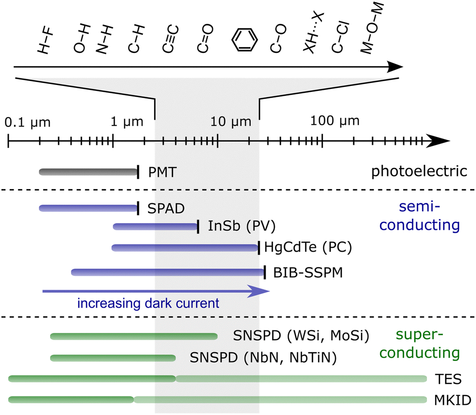 | ||
| Fig. 1 Overview of the typical spectral range covered by a selection of photodetectors relying on the photoelectric effect, semiconductors and superconductors as indicated by the coloured horizontal bars. A vertical bar at the long wavelength end indicates the upper limit imposed by the material's band structure for photocathodes and semiconductors, whereas the wavelength related to the energy gap in low-temperature superconductors is beyond the scale shown here. MKIDs and TESs essentially span the complete spectral range shown here but single-photon sensitivity above 1.55 and 4 μm, respectively, has yet to be demonstrated, as implied by the lighter green colour. Note that for SNSPDs, the upper edge of ∼10 μm does not correspond to a fundamental limit and only reflects currently accessible wavelengths. The region between 2.5 and 25 μm, highlighted in grey, indicates the spectral region where most fundamental vibrational frequencies are found. Selected examples of group frequencies are shown in addition.8 PMT: photomultiplier tube; SPAD: single-photon avalanche photodiode; PV: photovoltaic; PC: photoconductive; BIB-SSPM: blocked impurity band solid-state photomultiplier; SNSPD: superconducting nanowire single-photon detector; TES: transition edge sensor; MKID: microwave kinetic inductance detector. | ||
With their inherently smaller energy gaps and unique operating mechanisms, superconducting infrared detectors have the potential to revolutionize mid-infrared detection for vibrational spectroscopy. In addition, they also operate not much below the cryogenic temperatures that are already required for the best performing semiconducting IR detectors.
Their potential for the mid- and even far-infrared also makes them interesting candidates for future space telescopes. Some mission concepts by NASA, such as the Origins space telescope (OST), already include plans for superconducting transition edge sensors (TESs) and microwave kinetic inductance detectors (MKIDs).9 Superconducting nanowire single-photon detectors (SNSPDs) are another class of promising candidates for mid-infrared instruments of future space telescopes, which will be important for the search for extra-terrestrial life through exoplanet spectroscopy.10
Despite the great potential of superconducting detectors for the mid-IR, most applications of these novel detectors have so far been outside the mid-IR range.11,12 However, recent advances in the development of SNSPDs for the mid-IR region have made possible the first applications in molecular spectroscopy.13–17 These and many additional experiments able to profit from such detectors will be highlighted throughout this review.
As the tutorial review is intended to be read by chemists at every level, it is organized as follows: Section 2 introduces fundamental concepts of (single) photon detection and general requirements for modern experiments relying on vibrational spectroscopy. Section 3 gives an overview of commonly used semiconducting IR detectors as well as the most important single-photon detectors for the UV/Vis to mid-IR range and discusses their limitations. Additionally, a short introduction to infrared detector arrays and cameras is given in Section 4. Section 5 introduces three types of superconducting IR detectors, explains their operating principles, and highlights current developments. In Section 6, the currently available studies in chemistry based on superconducting detectors are presented. Finally, Section 7 summarizes expected future developments of superconducting detectors and presents our analysis of other experiments and techniques that could profit from the implementation of such devices.
2. Fundamentals of photon detection and requirements in molecular science
This section introduces important definitions and concepts, which will be used to discuss advantages and shortcomings of different detector types throughout this review. It provides a glossary of important concepts to those, not necessarily experts in detector physics, who are seeking the best detector for use in mid-infrared spectroscopy applications. A more complete overview for the reader who wishes to delve deeper can be found in ref. 18. In addition, Section 7 and Table 1 provide a quantitative discussion of detector requirements, which will only briefly be discussed here.| Figure of merit | Amorphous SNSPD (WSi, MoSi) | Polycrystalline SNSPD (NbN, NbTiN) | TES | MKID | Requirements for IR emission experiments |
|---|---|---|---|---|---|
| a Saturated internal efficiency (∼100%) up to 7.4 μm. The 50% value refers to the peak SDE expected for optical stacks optimized for different wavelengths within the 2–10 μm range based on simulations.10 b Saturated internal efficiency (∼100%) up to 3 μm and 80% for 4 μm. | |||||
| Wavelength range (single-photon sensitivity) | 0.3–10 μm32,33 | UV – 4 μm34,35 | <4 μm36 | <1.55 μm37 | 2.5–25 μm |
| System detection efficiency | 98% (1550 nm)38 | 99.5% (1350 nm)39 | 98% (805 nm)41 | 17%43 | ≈100% |
| 50%a (2–10 μm)10,33 | 98% (1590 nm)40 | 98% (850 nm)42 | |||
| 70%b (2000 nm)34 | |||||
| Timing jitter | 10.3 ps (1550 nm)44 | 4.3 ps (1500 nm)47 | 25 ns (850 nm)48 | 1 μs (1550 nm) | 1–100 ps |
| 76 ps (1550 nm)45 | 14.3 ps (2000 nm)34 | 4.1 ns (1550 nm)49 | |||
| 150 ps (1550 nm)46 | |||||
| Dark counts (counts s−1) | 0.0132 | 0.151 | 0.0652 | — | <0.01–1 |
| 0.008653 | |||||
| 0.00000650 | |||||
| Maximum count rate (counts s−1) | 107![[thin space (1/6-em)]](https://www.rsc.org/images/entities/char_2009.gif) 45 45 |
1.5 × 10955 |
10553,56 |
2 × 10343 |
106–108 |
| 1.2 × 10⁹ (64 pixel array)54 | |||||
| Number of pixels | 102457 | 6458 | 3660 | 202443 | — |
| 2044061 |
|||||
| 59059 | |||||
2.1. Sensitivity
The sensitivity of a detector is determined by its signal-to-noise ratio (SNR), which is simply the ratio of the absolute signal level to the detected noise. A related quantity is the noise equivalent power (NEP), which describes the power of incident light (P, in Watts) needed to generate a signal equal to the noise level (SNR = 1) for an electrical bandwidth, Δν = 1/(2τint), of 1 Hz (equivalent to ½ second of integration time, τint):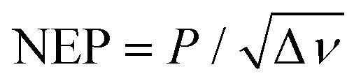 | (1) |
 | (2) |
2.2. System detection efficiency (SDE)
The system detection efficiency describes the overall probability that a photon emitted by the investigated sample or light source will be detected and is influenced by three factors (SDE = internal efficiency × absorption efficiency × coupling efficiency). Internal efficiency (sometimes referred to as quantum efficiency) describes the probability that an absorbed photon produces a detectable event, e.g. by releasing photoelectrons, exciting electrons to the conduction band in a semiconductor or inducing a normal-conducting state in a superconductor. As the name would suggest, absorption efficiency describes the probability that a photon reaching the detector will be absorbed. The coupling efficiency describes the probability that a photon emitted by the investigated sample or light source will reach the detector. It can be limited by geometrical constraints, e.g. the acceptance angle of the collection optics or a mismatch between the detector area and the cross section of an optical fiber, as well as reflection and absorption losses. Note that detectors are often characterized using setups with optimized coupling efficiency, for which SDEs near 100% are achieved. We emphasize that the SDE will often be reduced in a spectroscopic setup where additional optical components may be required.2.3. Noise
 :
:| P(k counts) = Nke−N/k! | (3) |
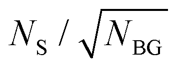
 . The total noise is determined by both signal (NS) and background counts (NBG).
 | (4) |
Accordingly, the SNR is given by:
 | (5) |
 . The ideal case (NS ≫ NBG) still involves shot noise arising from the detected signal and the SNR is given by
 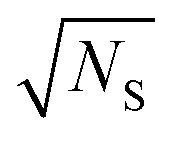 . Note that photon noise can always be reduced with increased integration time τint; here, the SNR scales with τint1/2.
The NEP of a shot noise-limited photon-counting detector at wavelength λ is given by:19
 | (6) |
2.4. Timing jitter
Jitter refers to temporal fluctuations in the rising edge of the measured electrical signal, which produce an uncertainty in the arrival time of the detected photon. Detector jitter ultimately limits the achievable time resolution of experiments relying on photon detection and therefore directly relates to the timescales of molecular processes that can be studied with that detector. Radiative lifetimes of vibrations are typically on the ms timescale; however, the timescales of many vibrational energy transfer processes can be much shorter and thus require comparably small jitter down to picoseconds.2.5. Stability
All detectors utilize some form of signal amplification (gain) in their operation, which may fluctuate over the timescale of the experiment. Gain fluctuation can be caused by small variations in temperature, bias voltage or bias current, limiting the stability of the measurement. These fluctuations are important to minimize in high-sensitivity experiments where long integration times over several hours are necessary. Such experiments include astronomical observations or single molecule spectroscopy, for example.2.6. Maximum count rate (MCR)
After a detection event, most photon detectors exhibit dead time, the time required before another photon can be detected. This limits the maximum count rate (MCR) of the detector. When exceeding the MCR, the detector saturates and produces non-linear signals, which are no longer proportional to the incident photon flux. Low MCRs may thus limit the SNR that can be obtained for a given integration time or prevent operation when background count rates are high.3. Conventional detector technologies
3.1. Semiconductor-based infrared detectors
Photodetectors based on intrinsic (pure) semiconductors, rely on the internal photoelectric effect, where photon absorption produces free charge carriers – electrons in the conduction band or holes in the valence band – capable of producing an electrical signal (see Fig. 2a). Obviously, it is impossible to detect a photon whose energy is less than the bandgap, limiting the maximum detectable wavelength for intrinsic semiconductors. Doping with extrinsic semiconductors (Fig. 2b–d) can be used to manipulate the band structure–extending the sensitivity to longer wavelengths.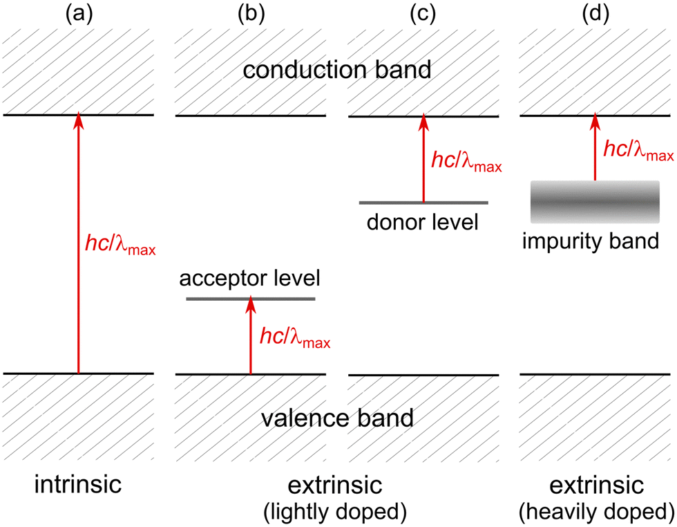 | ||
| Fig. 2 Schematic of the band structure in different types of doped semiconductors: (a) an undoped (intrinsic) semiconductor; (b) a p-doped semiconductor at low dopant concentrations; (c) an n-doped semiconductor at low dopant concentrations; (d) an n-doped semiconductor at sufficiently high dopant concentrations to form an impurity band. Red arrows indicate the lowest energy photon that can be absorbed in each type of semiconductor, giving rise to a long-wavelength limit of λmax. | ||
Doping introduces additional energy levels associated with the impurity atoms that are located between the valence and conduction band. For p-type semiconductors, acceptor levels lie close to the valence band, allowing electron excitation to the acceptor levels, leaving holes in the valence band that are the primary charge carriers (Fig. 2b). For lightly doped n-type semiconductors, donor levels close to the conduction band allow excitation of electrons from impurity levels to the conduction band and those electrons become the primary charge carriers (Fig. 2c). Higher levels of n-doping, necessary to achieve strong photon absorption, lead to overlap of the donor electron wavefunctions producing an impurity band (Fig. 2d), as discussed later in more detail.
Semiconductor-based photoconductive and photovoltaic detectors, whose operating mechanisms can be found in ref. 20, are commonly integrated in standard mid-infrared applications, such as FTIR spectrometers or other types of IR absorption experiments. They are easy to use as typically neither complex electronics nor thermal shielding is required. The detectors are available at moderate cost and cooling can be achieved with liquid nitrogen. Commonly used materials are InSb, which is sensitive out to ∼5.5 μm (1800 cm−1), or HgCdTe (MCT), whose bandgap energy depends on the Hg/Cd ratio in the Hg1−xCdxTe alloy20 and can be used to produce bandgaps as small as ∼0.05 eV providing sensitivity in the mid-IR. However, large dark currents remain a problem when attempting to access low vibrational frequencies in the so-called “fingerprint” region below ∼1500 cm−1 and limit their performance to peak D* values on the order of 1010 to 1011 cm Hz1/2 W−1.
3.2. Conventional single-photon detectors
In contrast to photoconductive and photovoltaic detectors, which convert a stream of incident photons into measurable voltages and currents, single-photon detectors detect individual light particles. Historically, the key feature of all well-established single-photon detectors is the electron multiplier, where a single electron produced by a single photon is detected in an avalanche-like process. We next discuss three specific devices used in the UV/Vis to mid-IR region. An excellent overview of other types of single-photon detectors can be found in ref. 21.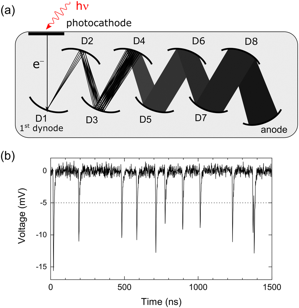 | ||
| Fig. 3 (a) Schematic design and operating principle of a photomultiplier tube. A single photon hitting the photocathode ejects a photoelectron that is repeatedly amplified through formation of multiple secondary electrons at each dynode (D1–D8). The amplified electron current is collected by the anode. (b) Simulated voltage output at the anode of a PMT. The pulses are assumed to arrive at an average rate of 107 counts s−1 with an average pulse height of 10 mV, where white noise was added to each point. The dotted line indicates a threshold at which all observed pulses would be detected in a pulse counting experiment. | ||
Achieving high sensitivity requires background elimination; optical shielding or even “lights out” operation may be required. The PMT sensitivity is ultimately limited by dark counts, produced by thermally induced electron emission from the photocathode. For cooled PMTs, dark count rates can be on the order of 1 s−1,21 making them highly sensitive single-photon detectors. However, PMTs are only useful when the photon energy exceeds the work function of the photocathode material, limiting their use to wavelengths shorter than ∼1000 nm.
The key advantage of single-photon counting is easy operation within the photon noise limit, as illustrated in Fig. 3b by a simulated PMT pulse sequence. Although the shape of individual pulses is altered by detector noise and the pulse amplitude varies due to gain noise, each peak can be clearly identified. By setting a proper threshold, high efficiency counting electronics can convert the signal into time-resolved photon counts, where detector noise and signal fluctuations become irrelevant. Note, however, that the absolute photon flux must be kept below a maximum count rate that is small enough to avoid pulses overlapping in time.
In single-photon avalanche photodiodes (SPADs), this avalanche process produces “clicks” from individual photons when a saturation current is reached. However, because of the saturation, the bias voltage must be reset after every detection event resulting in a significant dead time. The dead time may be aggravated by after-pulsing, where electrons that were caught in trap sites within the gain region are released during the detector reset and trigger a second avalanche. This is especially severe for the infrared where it can lead to dead times of up to 10 μs.21 Such a dead time limits the maximum counting rate. SPADs are available for the UV/Vis to near-IR region, where their detection efficiency, temporal response and dark count rates compete with the properties of PMTs.21 They are, however, far superior to PMTs in imaging applications within SPAD arrays (see Section 4).
The blocked impurity band solid-state photomultiplier (BIB-SSPM) overcomes this problem. A thin undoped blocking layer (BL) is introduced in contact with a heavily doped infrared-active layer (IRL). This is shown in Fig. 4(a) for a Si:As BIB-SSPN as developed by Petroff et al.26 In that device, n-doped silicon is used for the IRL, where arsenic serves as an electron donor (D → D+ + e−). Typical donor concentrations are 5 × 1017 cm−3. During growth of the IRL, a second acceptor dopant (A + e− → A−) is added at about 1/1000th the concentration of the donor. This results in similar concentrations of D+ and A−. While the D+ charges are mobile due to impurity band conduction, the A− cores are immobile. When a positive bias voltage is applied to the device, the concentration of mobile D+ charge carriers is therefore depleted within a few μm at the IRL/BL interface, while the A− concentration remains unchanged (Fig. 4b). This produces a strong electric field within the depletion region (Fig. 4c). This depletion region, if carefully grown and properly biased, can serve as a gain region, similar to that of a SPAD (see Fig. 4d). Electrons created by photon absorption in the IRL first drift toward the gain region, where they are accelerated to sufficiently high energies to cause multiple impact ionization of neutral donor atoms D. The secondary electrons then travel through the BL and are detected. The Si:As BIB-SSPM exhibits high gain (∼4 × 10⁴) as well as short pulses (∼1 μs) that make high count rates and sub-microsecond response possible.26
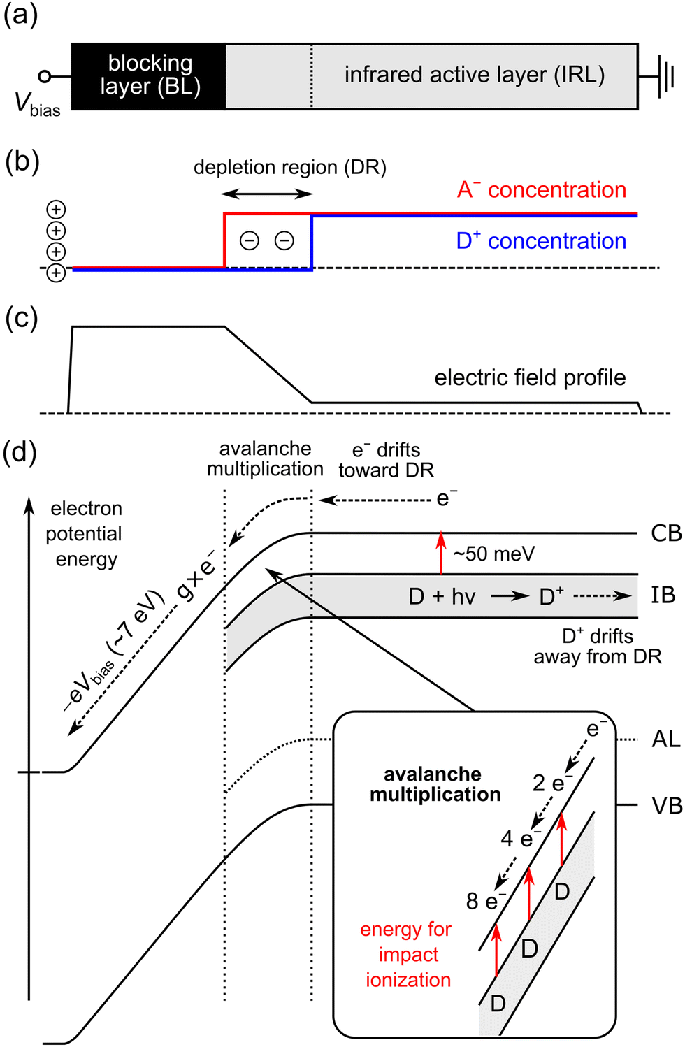 | ||
| Fig. 4 (a) Structure of a blocked impurity band solid-state photomultiplier (BIB-SSPM) according to Petroff et al.26 The blocking layer (BL) is composed of intrinsic silicon while the infrared-active layer (IRL) is strongly doped with a high concentration of As and a smaller concentration of an acceptor. The BL is held at a positive bias voltage while the IRL is connected to ground. Ohmic contact layers are not shown. (b) Concentration profiles of the ionized donor (D+, blue curve) and acceptor (A−, red curve) concentrations under positive bias. Negative charges indicate space charge due to the existence of A− in the D+ depletion region. (c) The electric field profile resulting from the concentration profiles in panel (b). (d) Schematic operating principle of a BIB-SSPM in terms of the band structure at the biased BL-IRL interface. Note that the avalanche multiplication process is similar to that occurring in the depletion region of a SPAD. CB: conduction band edge, IB: impurity band, AL: acceptor level, VB: valence band edge. | ||
In our opinion, BIB-SSPMs represent the best solid-state analogue of a PMT in the mid- to far-infrared region. Limitations of BIB-SSPMs are related to dark counts from thermal ionization of the donor atoms, even at 7 K. In addition, the statistical nature of the avalanche multiplication leads to excess gain noise, although the distribution of gain values is relatively narrow.25 BIB-SSPM setups also require low operating temperatures and good thermal shielding (see Section 7.2.3) compared to PMTs or SPADs, conditions close to those needed for superconducting detectors.
4. Detector arrays and cameras
Combining the discussed types of infrared detectors into large one- or two-dimensional detector arrays, also often called focal plane arrays (FPAs), allow position-dependent measurements, where the signal from single detector pixels is read out individually. A comprehensive review of common FPA read-out mechanisms, such as the popular charge-coupled devices (CCDs) and complementary metal-oxide-semiconductor (CMOS) sensors, which essentially combine many photodiodes on a single substrate, is beyond the scope of this review. The reader is referred to ref. 20 and references therein.Such detector arrays can be used in infrared cameras with various applications in astronomy, infrared microscopes, thermographic imaging, etc. Another application includes their use in spectrographs, which can simultaneously detect a range of wavelengths and offer an improved SNR (multiplex advantage) over spectrometers based on scanning monochromators, which detect a single wavelength at a time. An important example is the echelle spectrograph, which allows to simultaneously detect different wavelengths at different positions on the detector array and is primarily used in astronomical telescopes.27 Detector arrays capable of single-photon detection together with echelle spectrographs would also be interesting candidates for physical chemistry laboratory experiments instead of the more commonly used scanning monochromators. In addition, combining multiple detector pixels can increase the effective size of the detector when the size of efficient single detector pixels is limited by the manufacturing process.
The highest performing infrared detector arrays are typically found in ground- and space-based infrared telescopes, as those impose stringent requirements on their sensitivity to distinguish small signals against large background noise. A recent example is the James Webb Space Telescope (JWST) launched in December 2021.28 It contains four infrared instruments: three near-IR instruments, operating in the range 0.6–5.0 μm, and one mid-IR instrument operating in the range 5–28 μm.29 The near-IR instruments (a camera, a spectrograph and a guidance sensor) all employ multiple 2048 × 2048 hybrid MCT array detectors (Teledyne H2RG) that are operated at ∼35 K, achieved by passive cooling. The mid-IR instrument, on the other hand, uses 1024 × 1024 arrays of Si:As BIB detectors for its mid-infrared camera and spectrometer, which are actively cooled to 7 K with a cryocooler.
Note that the JWST arrays are not capable of single-photon counting. For example, pure BIB detectors are used in the JWST, which differ from BIB-SSPMs in terms of lower acceptor concentrations and smaller bias voltages in order to extend the depletion region for efficient charge extraction and to avoid gain noise due to avalanche multiplication.30 Smaller SPAD arrays, on the other hand, combine the high sensitivity and temporal resolution of single-photon counting with spatial resolution.31 However, just as single-pixel SPADs, they are not sensitive in the mid-infrared, which leads us to the discussion of superconducting single-photon detectors in the mid-infrared including possible array sizes.
5. IR detectors based on superconductivity
5.1. Physical mechanisms
Superconductivity arises due to the weak attraction between electrons induced by lattice distortions, which can outweigh the Coulombic electron-electron repulsion at large distances. These attractive forces allow two electrons of opposite momentum and spin to form stable “electron dimers”, known as Cooper pairs.62 The Cooper pairs, having zero spin, are bosons and can undergo Bose–Einstein condensation leading to superconductivity.Superconductivity is only possible when Cooper pairs are stable, appearing below a critical temperature (Tc), current density (Jc) and magnetic field (Bc). If any of these three quantities is exceeded, normal conductivity will arise. The energy required to dissociate a Cooper pair, 2Δ ≈ 3.25kBTc, can be estimated from Bardeen–Cooper–Schrieffer (BCS) theory.62 Thus, even a 1.1 mm wavelength photon could destroy a Cooper pair in a superconductor with Tc = 4 K. A mid-infrared photon, possessing 100–1000× more energy, can destroy far more.
This simple picture makes it possible to envision how absorption of a single mid-IR photon might raise the effective local temperature enough to induce switching from superconductivity to normal conductivity, a fundamentally novel “amplification” mechanism that provides two key advantages. The first is the small effective energy gap with the promise of long wavelength sensitivity. The second is ultra-low detector noise due to low dark count rates, which is intrinsic to low-temperature superconducting materials.
5.2. Superconducting nanowire single-photon detectors (SNSPDs)
SNSPDs are perhaps the simplest and most promising implementation of these ideas and have recently emerged as the highest-performing single-photon detectors for time-correlated single-photon counting from the ultraviolet to the mid-infrared.32,33,38 Their excellent performance, especially for mid-infrared applications, is summarized in Table 1 and compared to the performance of other superconducting single-photon detectors introduced in this review. SNSPDs based on amorphous superconductors have demonstrated 98% system detection efficiencies at 1.55 μm, dark count rates as low as 1 count per day, zero readout noise, and count rates higher than 107 counts s−1 pixel−1.38,50 This was achieved at a typical time resolution of 100 ps, which can be even as low as a few picoseconds in exceptional cases.44,47 Note, however, that not all of these outstanding characteristics are necessarily achieved in the same device, which is specifically highlighted by comparing SNSPDs based on amorphous and polycrystalline materials in Table 1. Amorphous SNSPDs do not yet achieve the maximum count rates and timing jitters of polycrystalline SNSPDs. Nevertheless, except for the sensitivity being so far limited to wavelengths shorter than 10 μm—a limitation that is likely to be soon overcome—the current characteristics of amorphous SNSPDs are already close to the requirements for state-of-the-art infrared emission experiments, as discussed in Section 7.2.1. We next discuss SNSPD performance characteristics in detail.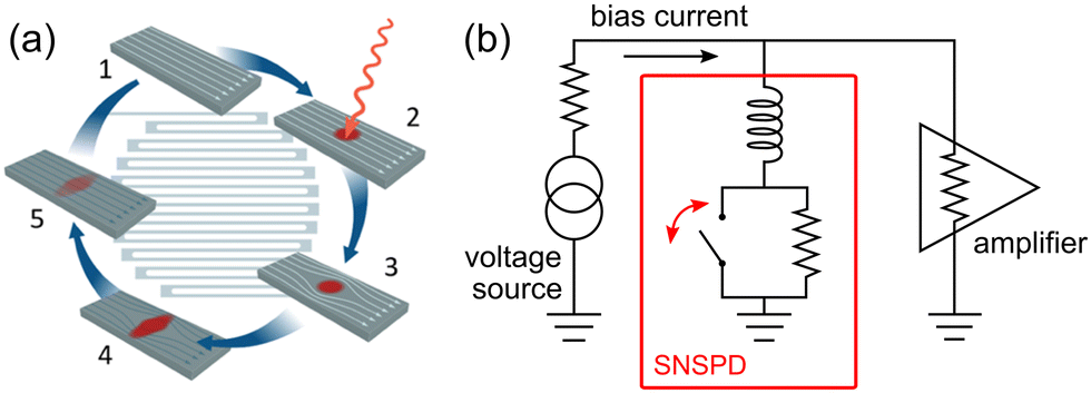 | ||
| Fig. 5 (a) Conceptual representation of the operating principle of an SNSPD. The details are explained in the text. (b) Schematic of a typical readout circuit for SNSPDs. The nanowire acts as a switch which opens when the photon is absorbed, causing the bias current to be shunted into the readout amplifier. | ||
To a first approximation, the superconducting wire thus acts as a switch in parallel with a large resistance, which opens when the photon is absorbed, as illustrated in Fig. 5(b). This pushes the current out of the nanowire and into the readout circuit, which comprises a 50 Ω amplifier chain. After the current is diverted, the nanowire cools off, returning to the superconducting state, and current rebuilds in the nanowire on a time scale of 10 ns. At this stage, the device is ready to count another photon.
While the operating concept is simple, SNSPD fabrication challenges have taken decades to overcome. The first SNSPDs were fabricated in 2001 from 5 nm thick NbN superconducting films, and consisted of 200 nm wide and 1 μm long microbridges operated at a temperature of 4.2 K.65 NbN is well studied in superconductivity research and was chosen due to its high Tc (9–12 K). Unfortunately, NbN is polycrystalline and the presence of many grain boundaries can lead to poor uniformity over large areas. Hence, fabrication required lattice matching to the film-growth substrate and high growth temperatures. These limitations constrained fabrication of high-efficiency devices for many years.
Ten years after the first report, experiments began on the fabrication of SNSPDs based on amorphous superconductors.66 In contrast to NbN, amorphous superconductors lack grain boundaries as they are highly disordered glasses. This leads to an extremely useful property – amorphous superconducting materials can be sputtered at room temperature on any sufficiently smooth substrate and have excellent uniformity over large areas. The use of amorphous superconductors such as WSi and MoSi eliminated many constraints on fabrication, and for the first time allowed the production of large area, high efficiency devices.46 Also the low fabrication temperature was especially helpful because optical stacks based on metallic mirrors could be used (vide infra) and integration with other room temperature manufacturing processes was simplified.
We note that more recently SNSPDs based on polycrystalline NbTiN and NbN sputtered at room temperature have also resulted in high detection efficiency.39,40 Furthermore, efforts to improve sensitivity of NbN and NbTiN-based SNSPDs at mid-infrared wavelengths are ongoing and significant progress has been made recently.34,67 This tutorial is focused primarily on amorphous WSi-based SNSPDs as these have been implemented in mid-IR physical chemistry experiments. NbN and NbTiN-based SNSPDs should be considered a mid-IR option in the future as they have certain advantages, such as better timing resolution and higher maximum count rates.
First, internal efficiency describes the probability that a photon absorbed by the nanowire will produce an electrical pulse. It is strongly influenced by the physics occurring during the amplification of the initial hotspot, which depends on the superconductor's transition temperature, electron–phonon coupling strength, and thermal relaxation time. Fig. 6a shows measured SDEs vs. bias current for a WSi SNSPD from ref. 46. A typical feature of SNSPDs is that, at sufficiently high bias currents, the internal detection efficiency saturates – i.e., every absorbed photon produces a pulse. This saturation also reduces noise as the response becomes insensitive to fluctuations in bias current and temperature. Fig. 6a also shows the switching current, ISW, the current at which the critical current density is exceeded, and the cutoff current, ICO, defined as the current at the inflection point of the curve. ICO is, roughly speaking, the bias current at which the SNSPD “turns on” and it becomes larger for longer wavelengths, eventually requiring operation near ISW (see Fig. 6b).
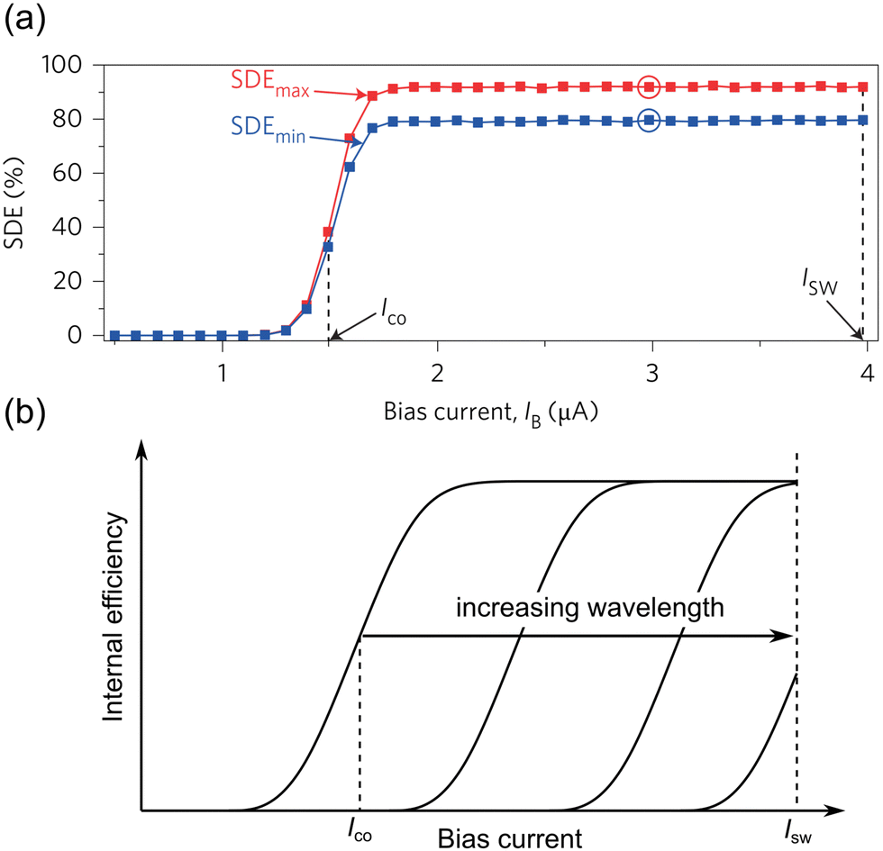 | ||
| Fig. 6 (a) Plot of system detection efficiency (SDE) vs. bias current for a typical WSi-based SNSPD. SDEmax (red) corresponds to illumination with light polarized parallel to the nanowire orientation. SDEmin (blue) corresponds to illumination with light polarized perpendicular to the nanowire orientation. The SDE for the two polarizations differs because the meander structure acts effectively as a diffraction grating. The switching current (ISW) and cut-off current (ICO) are also indicated. Adapted with permission from ref. 46. Copyright 2013 Nature Publishing Group. (b) Schematic wavelength dependence for the internal efficiency of an SNSPD. The cut-off current and the onset of the plateau shift to higher bias currents with increasing wavelength. For the highest wavelength curve shown here, the SNSPD switches to the normal-conducting state before the plateau is reached. | ||
The second factor affecting SDE, the absorption efficiency, describes the likelihood that a photon incident upon the nanowire is absorbed. Fig. 7(a) shows how absorption is enhanced using an optical stack with an embedded SNSPD.38 Typically, a gold mirror is combined with a 1/4-wave layer of SiO2 underneath the SNSPD and an antireflection coating deposited on top. To avoid the intrinsic ∼3% absorption of a metallic mirror, one can instead use a distributed Bragg reflector (DBR) consisting of alternating layers of two materials with different dielectric constants, as shown in Fig. 7(b). SNSPDs with SDEs greater than 98% have recently been demonstrated using DBR back reflectors.38 Here, the ability to deposit the amorphous superconductor on any substrate is especially helpful. SNSPDs based on NbN and NbTiN have also demonstrated better than 98% SDE at 1550 nm wavelength.39,40
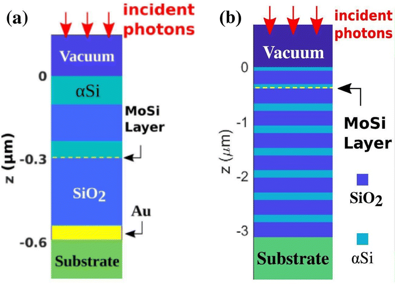 | ||
| Fig. 7 (a) Optical stack of a typical high-efficiency SNSPD utilizing a metallic mirror. (b) Optical stack of a high-efficiency SNSPD utilizing a distributed Bragg reflector (DBR) instead of a metallic mirror. Here, MoSi is used as the superconductor but in principle any superconductor could be used in such a stack. Panels (a and b) adapted with permission from ref. 38. Copyright 2020 Optical Society of America. | ||
Finally, high SDEs require optimized coupling efficiency between the experiment and the active area of the detector. In principle, SNSPDs can be either free-space coupled or fiber-coupled, whereby the latter is often preferred in practice as it avoids the need for cryogenically cooled mirrors and lenses. Furthermore, since SNSPD chips can be precisely micro-machined to fit into commercially available zirconia sleeves they become essentially self-aligning when used in combination with fibers (see Fig. 8a).68 Modern SNSPDs have a diameter of 20–50 μm, while the mode field diameter of a 1550 nm single-mode optical fiber is approximately 10 microns. Alignment tolerance using the self-aligned coupling technique is ±3 microns. Fig. 8(b) shows the device chip in detail. The active area of the SNSPD lies at the center of the 2.5 mm circle, with gold leads carrying the bias current and electrical pulses leading out from the SNSPD onto the “diving board” of the silicon chip. This now standard design works well and is highly robust. Extending this design to the mid-IR requires modified fibers which we will discuss below (Section 6.1).
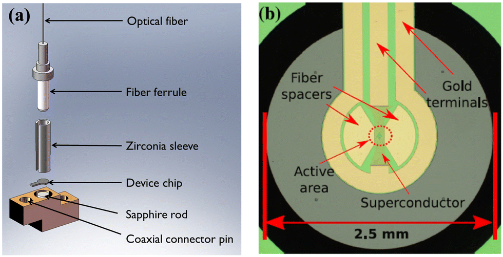 | ||
| Fig. 8 (a) Illustration of the self-aligned device package used for fiber coupling. (b) Optical micrograph of the device chip, showing the circular chip which is precisely etched to the dimensions of the zirconia sleeve, which is 2.5 mm in diameter. The SNSPD active area at the center of the circle and gold leads are also indicated. Reprinted with permission from ref. 38. Copyright 2020 Optical Society of America. | ||
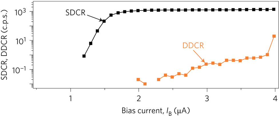 | ||
| Fig. 9 Plot of the system dark count rate due to background photons (SDCR, black) and the device dark count rate (DDCR, orange) of a typical fiber-coupled SNSPD. Note that near 4 μA the switching current is reached. Adapted with permission from ref. 46. Copyright 2013 Nature Publishing Group. | ||
Reducing the effects of background leak into the fiber and blackbody radiation emitted from the fiber itself can be achieved by tightly coiling the optical fiber (coil diameter of ∼35 mm, 5–6 loops), which leads to a high loss for low energy blackbody photons. For light at 1550 nm, only a few percent loss was seen. This technique can reduce background rates by an order of magnitude or more depending on the experimental setup and number of loops in the fiber coil.45,69,70
For operation in the mid-infrared, cryogenic shielding is required (see Section 6.1). Without shielding blackbody radiation alone can easily result in count rates so large that the detector latches into the normal conducting state and cannot be operated.
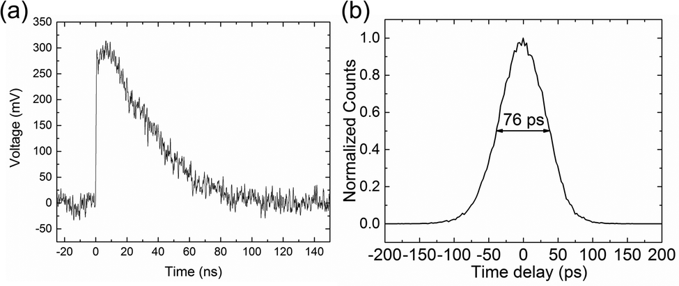 | ||
| Fig. 10 (a) Electrical pulse from a MoSi SNSPD. (b) Jitter histogram of the same SNSPD. The full width at half maximum of 76 ps characterizes the magnitude of jitter. (a and b) adapted with permission from ref. 45. Copyright 2015 Optical Society of America. | ||
Jitter is influenced by amplifier noise, geometric jitter, and intrinsic jitter.71 Intrinsic jitter is the result of statistical variations in the time it takes for the hotspot to form and grow within the nanowire and depends on the superconducting material's electron–phonon scattering time, electron–electron scattering time, as well as the thermal coupling between the superconductor and substrate. Further degradation of the intrinsic jitter results from the rise time dependence on the ratio Lk/Rk, where Lk is the kinetic inductance (see Section 5.3.2) and Rk is the hotspot resistance of the nanowire. Larger detectors with increased active area and longer nanowires show larger Lk values and slower rise times. Intrinsic jitter is typically the smallest contributing factor to the overall jitter.
Geometric jitter arises because a meandering superconducting wire acts as a microwave transmission line, resulting in a small but finite propagation time from the hotspot to the amplifier.71 This propagation delay varies depending on where along the wire the photon is absorbed. This contribution to jitter is proportional to the total length of the nanowire (size of the detector) and typically the second largest contribution to jitter.
Amplifier noise is the final contributing factor to arrival time uncertainty. To minimize this in experiments demanding the lowest possible jitter, cryogenic amplifiers are critical.
An upper limit to the MCR is determined fundamentally by the physics of the thermal relaxation process after generation of the hotspot – the shorter the thermal time constant, the higher the MCR. Epitaxial superconductors on lattice-matched substrates, e.g. NbN on MgO, provide MCRs on the order of 100 MHz–1 GHz, due to stronger electron–phonon coupling in the superconductor and thermal coupling between the superconductor and its substrate. SNSPDs based on amorphous superconductors are typically limited to ∼10 MHz.
Often the electrical relaxation time, τel, is longer than the thermal time constant and limits the MCR instead. Fig. 10(a) shows an example of a measured SNSPD pulse with a τel of 35 ns.45 The electrical relaxation time is determined by Lk/R, where R is the resistance of the readout circuit (typically 50 Ω). For similar reasons as discussed in Section 5.2.4, τel can thus be reduced by decreasing the size of detector pixels.
5.3. Alternatives to SNSPDs
While SNSPDs have many advantages, there are other technologies that one should be aware of, which we now discuss briefly.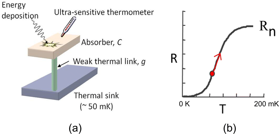 | ||
| Fig. 11 (a) Cartoon model of a transition edge sensor. (b) Diagram of the operating point in the superconducting transition. The red arrow indicates the change in resistance caused by the energy of the photon(s) absorbed in the detector. | ||
Despite these issues, TESs are excellent detectors especially where photon number or energy resolution is needed – keep in mind that the magnitude of the resistance change is a direct readout of the absorbed energy. TES efficiencies can be above 95% in the optical and near-IR.73 They are single-photon sensitive from the X-ray to 4 μm, and can also be used to characterize the energy of massive particles instead of photons. Work is also in progress to improve their MCR and jitter.49
Furthermore, small arrays have been demonstrated, typically with less than 100 pixels,74 and work on larger arrays approaching 1 kilopixel is ongoing. However, the necessity of SQUIDs for read-out make multiplexing for arrays more complex; this accounts for current limitations on array size. Pixel sizes vary widely – 20 μm to several hundred microns – depending on the target photon energy and energy resolution requirements.
The ability to multiplex a large number of detectors is the primary advantage of MKIDs. Each pixel can be tuned to have a unique resonant frequency, thus allowing multiple pixels to be capacitively coupled and multiplexed to the same microwave readout line. One can then sweep the frequency on the readout line to sequentially interrogate each pixel.75 This enables very large arrays using only a few microwave transmission lines, an important advantage in cryogenic devices as each readout line carries an associated heat load. 1 kilopixel arrays are easily achievable and large MKID arrays are now being used routinely for ground-based astronomy.43
MKIDs have been widely used in astronomy, particularly in the UV to near-infrared and the far-infrared.75 Like TESs, MKIDs are energy-resolving detectors. However, single-photon sensitivity has only been demonstrated from the UV to the near infrared (up to 1550 nm wavelength) but not yet for the mid-to-far-IR. At 1550 nm, noise levels are comparable to those of typical SNSPDs (NEP ≈ 10−19 W Hz−1/2). Disadvantages of MKIDs include their lower operating temperature of ∼100 mK, which has so far prevented their use in space-based applications, smaller dynamic range (MCR ≈ 5 kHz pixel−1), lower efficiency, and the complexity of the room temperature readout electronics.
6. Superconducting detectors in Chemistry
6.1. A mid-infrared laser-induced fluorescence instrument
The first application of superconducting detectors for molecular spectroscopy has been recently reported, where a tunable mid-IR laser pulse (5 ns) excites a sample of CO adsorbed to a NaCl(100) crystal to detect time- and wavelength-resolved mid-IR fluorescence (IR-LIF). Details of the spectrometer design, shown in Fig. 12, can be found in ref. 13, 15, 16 and 76. The spectrometer comprises a homebuilt grating monochromator and a 4 × 1 SNSPD array (25 μm × 100 μm for each pixel) connected by a As2S3 multi-mode infrared fiber (IRF-S-100, IRflex). The WSi SNSPD (Tc ≈ 3.5 K) is cooled down to temperatures between 0.3 and 0.6 K, achieved with a two-stage 3He cryocooler (CRC-GL7-009, Chase Research Cryogenics), attached to the 4 K stage of another closed-cycle 4He cryocooler (RDK-101D, Sumitomo). The monochromator is connected to the 40 K stage of the 4He cryocooler and gold-coated aluminum plates, connected to the 4 K stage, shield the 3He cryocooler and the SNSPD. A second layer of aluminum shields is attached to the 40 K stage. Additionally, optical filters are used to further suppress blackbody emission from the sample's surroundings.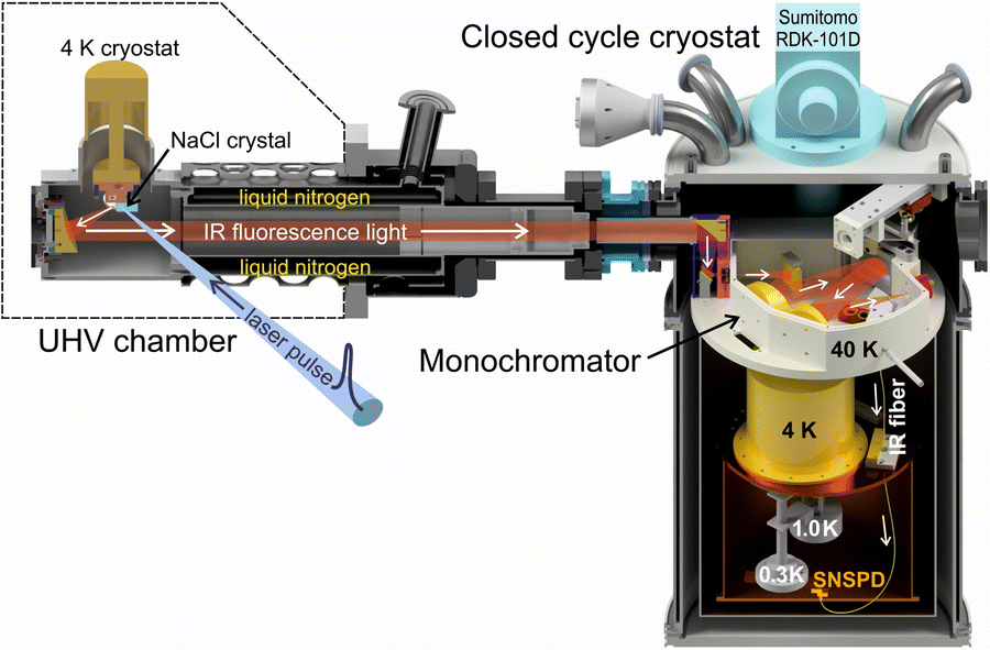 | ||
| Fig. 12 Overview of the infrared LIF setup based on a SNSPD. The left part of the setup shows an ultra-high vacuum chamber, shielded from thermal radiation by a liquid nitrogen cold shield, which is used for investigating CO molecules adsorbed to a NaCl crystal at cryogenic temperatures. The right part of the setup, separated from the UHV chamber by a CaF2 window, shows the completely independent spectrometer chamber containing a 40 K grating monochromator, which is connected to the 0.3 K cold SNSPD via a multi-mode mid-IR fiber. From ref. 13. Reprinted with permission from AAAS. | ||
The SNSPD bias current (∼5 μA) is supplied by an isolated voltage source (SIM928, Stanford Research Systems). SNSPD signal pulses are amplified by cryogenic amplifiers (SGL0622Z, Qorvo) attached to the 40 K stage and passed to a multi-channel scaler (MCS, model: MCS6A-2, FAST ComTec) with a resolution of 100 ps to record time-resolved photon counts with respect to the excitation laser pulse. This spectrometer demonstrated a temporal resolution of ∼500 ps.16 In many of the experiments discussed in the following, the time resolution was limited by the SNR. For example, for dispersed LIF experiments on a monolayer of CO, which had not been previously possible with conventional detectors,77 the MCS temporal binning was set to 1 μs to ensure an adequate SNR.17 Clearly, further improvements in the SNSPD sensitivity have the potential to allow measurements at shorter timescales.
One should note that the SDE of this setup is substantially smaller than that of the stand-alone SNSPD discussed in Section 5, where the SDE approached 100%. This is explained in ref. 16. The mismatch between the 100 μm wide fiber core and a single detector pixel (25 μm × 100 μm) alone gives a coupling efficiency of ηcouple = 0.2. In particular, the fluorescence collection factor, Fcoll = 0.005, which depends on the acceptance angle of the monochromator (16°), reduces the coupling efficiency further. Additional losses occur at the input to the multi-mode mid-IR fiber, ηfiber = 0.69, and due to optical transmission through the monochromator, Fopt ≈ 0.8. Assuming that the absorption efficiency and internal efficiency of the SNSPD are 1 for simplicity, all these factors together give an SDE of 5.5 × 10⁻⁴. For future experiments, in which a sufficiently large SNSPDs array without fiber coupling could be used, the SDE would improve to 4 × 10⁻³, mainly limited by the fluorescence collection factor.
6.2. Applications: Vibrational energy transfer studies of CO adsorbed on NaCl(100)
When a mid-IR laser pulse is used to excite a large fraction of CO molecules adsorbed to a NaCl surface to their first vibrationally excited state (v = 1), the vibrational dynamics are subsequently controlled by fast vibration-to-vibration (V–V) energy transfer processes in competition with relaxation to the salt crystal. Infrared emission spectroscopy in combination with kinetic Monte Carlo modelling is an ideal means to study these processes with time- and quantum state-specificity.17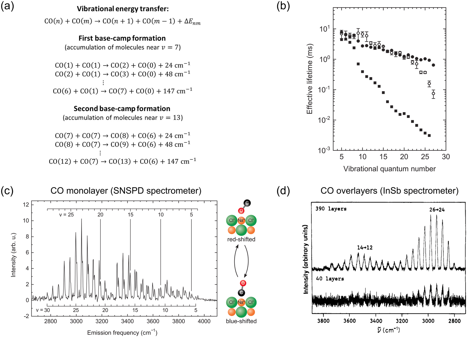 | ||
| Fig. 13 Vibrational energy pooling for CO adsorbed on NaCl(100). (a) Vibrational energy scheme demonstrating different energy transfer steps in the base-camp mechanism including the associated energy mismatch. Numbers in brackets indicate the vibrational quantum numbers of the CO stretching vibration. (b) Effective lifetimes obtained from ref. 17 for the millisecond decay of individual vibrational states of monolayer CO after vibrational energy pooling. Open circles indicate experimental values. Solid circles and squares correspond to effective lifetimes obtained from kinetic Monte Carlo simulations relying on the models for non-radiative long-range energy transfer (CPS model) and anharmonic coupling through the CO–surface bond, respectively. From ref. 17. Adapted with permission from AAAS. (c) Dispersed infrared emission spectrum of the CO monolayer on NaCl(100) after pulsed infrared laser excitation of CO(1) measured with the SNSPD-based spectrometer described in Section 6.1. The spectrum is integrated over the initial 200 μs after excitation and all transitions correspond to overtone transitions (v → v − 2). From ref. 13. Adapted with permission from AAAS. (d) Dispersed overtone emission spectra of CO overlayers of different thickness, epitaxially grown on NaCl, as measured by Chang and Ewing with a spectrometer based on a liquid nitrogen-cooled InSb detector. Adapted with permission from ref. 78. Copyright 1990 American Chemical Society. | ||
This continues until the amount of energy released exceeds the highest phonon frequency, above which a single phonon is not sufficient to compensate the energy defect involved in VEP. Here, the pooling stalls, establishing an intermediate “basecamp” at v ≈ 7. At this stage, only molecules in v ≈ 7 can exchange energy pushing a few molecules further up the ladder as others are de-excited (v = 7 + 7 → 8 + 6 etc.). This is again associated with small energy defects accepted by single NaCl phonons, but the v ≈ 7 molecules are on average farther from one another and so the VEP is slower. As VEP progresses, the energy defect increases again, and a second ceiling is hit when molecules reach v ≈ 14 whereby a second basecamp is produced. This process continues up to a third basecamp with the overall timescale for the successive formation of the basecamps ranging from ns to ∼100 μs. Fig. 13c shows a mid-IR fluorescence spectrum obtained from a CO monolayer sample undergoing VEP, where the intensity minima near v = 8 and 19 demarcate the three basecamps.
With the help of time-resolved IR-LIF measurements, the lifetimes of the individual vibrational states, which are on the millisecond timescale, could also be measured and compared to different models for energy loss from the CO vibration to the NaCl substrate.17 This comparison (see Fig. 13b) clearly showed that vibrational relaxation from CO to NaCl occurs through non-radiative long-range energy transfer instead of anharmonic coupling via the CO–surface bond, which would typically be expected to dominate but is less important here due to the weak CO-NaCl interaction.17 A relaxation model developed by Chance, Prock and Silbey (CPS model) described the observed rates well.79
The observation of the “upside-down” CO was only possible due to the sensitivity achieved with superconducting detector technology. Fig. 13d shows dispersed mid-IR fluorescence spectroscopy using a liquid-nitrogen cooled InSb detector from the seminal work of Ewing and co-workers.77,78 There, a comparable SNR required sample concentrations nearly 1000× higher than in the monolayer experiments using SNSPDs. Furthermore, detection of dispersed fluorescence from the monolayer could not be achieved by Ewing and co-workers while retaining a sufficient SNR for detailed experiments on vibrational energy transfer in the CO/NaCl system.77
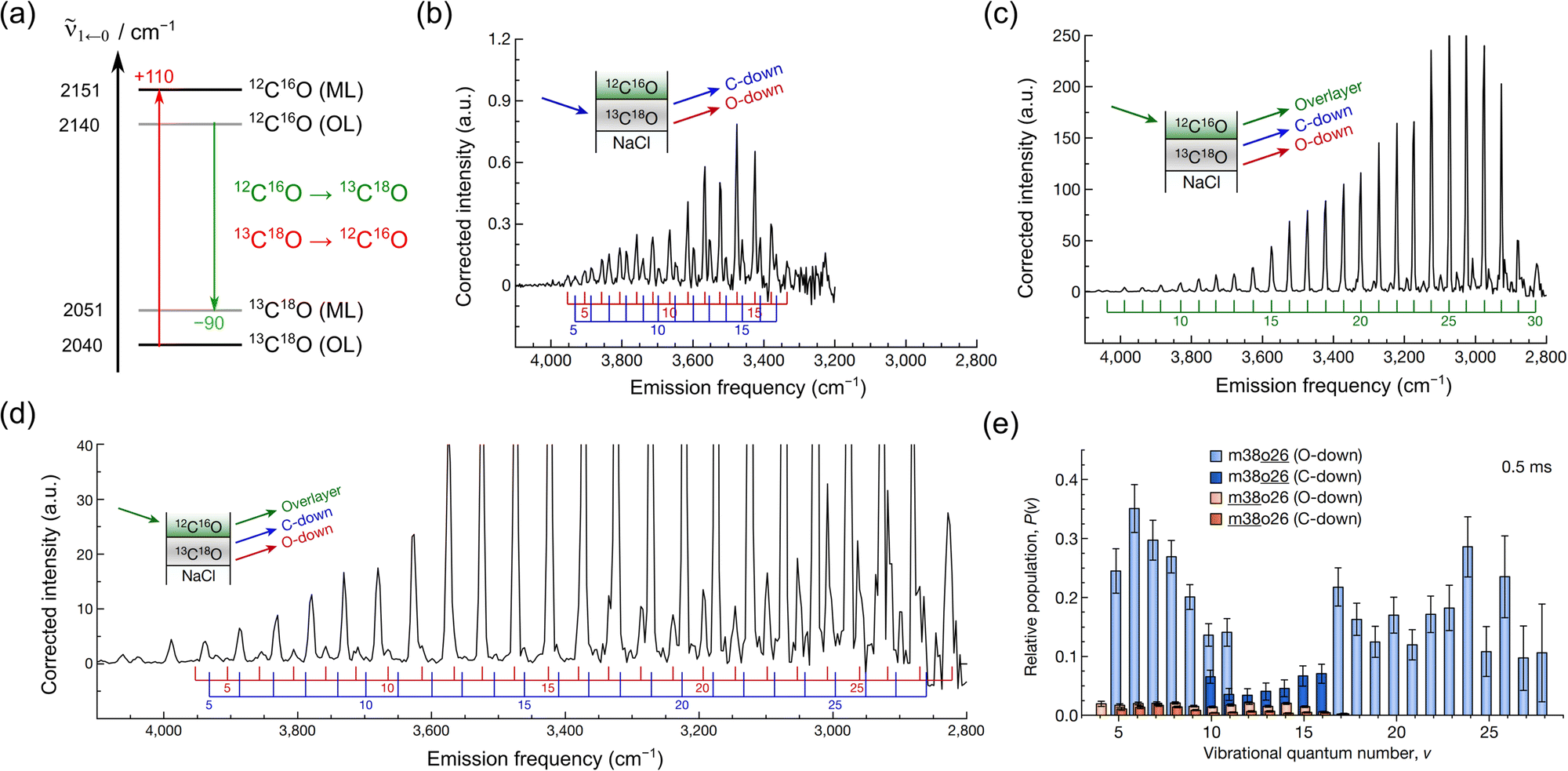 | ||
| Fig. 14 Interfacial vibrational energy transfer between different isotopically labelled CO layers. (a) Schematic infrared spectrum showing fundamental vibrational frequencies of 12C16O and 13C18O in the monolayer (ML) and overlayer (OL). (b) Overtone emission spectrum (v → v − 2) after selectively exciting the monolayer in the 13C18O (ML)/12C16O (OL) sample. (c and d) Different views of the overtone emission spectrum after exciting the overlayer in the 13C18O (ML)/12C16O (OL) sample. Throughout panels (b–d), the coloured combs together with the cartoons indicate the assignment of emission lines to different initial vibrational states, v, of the respective CO species. (e) Relative populations of different vibrational states of the C-bound and O-bound isomer in the monolayer after direct excitation of the monolayer (orange distributions) and indirect excitation via the overlayer followed by interfacial energy transfer (blue distributions). (b–e) adapted from ref. 14 with permission from Springer Nature. | ||
Fig. 14a also schematically indicates the expected direction of vibrational energy flow of the two 12C16O (ML)/13C18O (OL) and 13C18O (ML)/12C16O (OL) samples, based on the differences in the fundamental vibrational frequencies within the two layers, which differ by only ∼100 cm−1. Indeed, the expected direction of energy flow could be confirmed experimentally.14 For the 12C16O (ML)/13C18O (OL) sample, both excitation of the 12C16O monolayer and the 13C18O overlayer lead to emission from the 13C18O overlayer. The emission spectra after excitation of the other 13C18O (ML)/12C16O (OL) sample are shown in Fig. 14b–d. There, excitation of the 13C18O monolayer leads solely to emission lines associated with the O-bound and C-bound isomers in the 13C18O monolayer, as energy transfer to the 12C16O overlayers does not take place. Most importantly, excitation of the 12C16O overlayer also gives rise to emission lines from the O-bound and C-bound isomer in the 13C18O monolayer, in addition to emission from the overlayer itself, indicating efficient energy transfer from the 100 overlayers to the single monolayer.
In fact, conversion of the emission intensities to relative vibrational population for the monolayer and overlayer emission after overlayer excitation (Fig. 14e) indicates that about 12% of the vibrational quanta initially deposited into the overlayer are transferred to the monolayer. Since ∼50% of the overlayer molecules were initially excited by the IR laser, this equates to ∼1.5 eV vibrational energy per monolayer molecule. This highlights the large amount of energy concentrated in the monolayer by indirect infrared absorption through the overlayer,14 which can then drive the orientational isomerization from the C-bound to the O-bound orientation in the monolayer.
This phenomenon occurring in the infrared with vibrational states resembles light harvesting in biological systems using electronic states. Not only may it be possible to utilize this effect to transfer large amounts of energy to induce chemical reactions but the experiment also demonstrates the potential of the SNSPD-based spectrometer to study vibrational energy transfer dynamics.
6.3. Current development of detectors for exoplanet spectroscopy
As the number of discovered exoplanets continues to increase, the atmospheric composition of these planets has emerged as a topic of extreme importance. For example, infrared spectra of water, methane, ozone, carbon dioxide, and nitrous oxide could provide molecular signatures indicative of exoplanetary life. These compounds exhibit their own unique spectral fingerprint in the mid-infrared from 2.8–20 μm.When an exoplanet transits its parent star, a small fraction of the starlight passes through the planet's atmosphere. If this light could be spectrally analyzed, such molecules could be revealed. Due to the extremely low photon fluxes at the telescope and long transit times typically lasting several hours, single-photon detectors with zero readout noise, stability below 5 ppm, and efficiency of at least 50% are required. While BIBs and MCTs are also highly sensitive in the mid-infrared and operate at higher temperatures than SNSPDs, they are not stable at the 5 ppm level necessary for future spaceborne telescopes. BIBs also suffer from a number of undesirable effects such as reset anomaly, last-frame effect, droop, drift, multiplexer glow, and latent images.80 MKIDs also show promise in the mid-infrared, but are limited in dynamic range, stability and even lower operating temperatures, as discussed in Section 5.3.2. While TESs have been proposed for missions such as ORIGINS for use in the far-IR, they have not yet been optimized for the mid-IR.
Based on recent advances, SNSPDs show the greatest promise for exoplanet spectroscopy.10 They are currently the only detector which is truly single-photon counting in the mid-infrared, and there are reasons to believe that SNSPDs could meet the stringent stability requirements of 5 ppm or better. To date, saturated internal detection efficiency has been demonstrated up to a wavelength of 10 microns, for which simulations suggest that an overall SDE of 55% is realistic,33 and currently unpublished results for 64-pixel arrays optimized for the mid-infrared have also been obtained recently. Additional work is underway to extend sensitivity to longer wavelengths, to improve the overall SDEs of single pixels beyond 50% and to increase array sizes to at least 1 kilopixel. While SNSPDs were not specifically considered as a relevant technology in the 2020 NASA Decadal Survey for missions such as OST, NASA is now funding SNSPD development and it will likely be considered in future surveys as the technology continues to progress.
7. Prospects for the future
In this final section of the tutorial review, we outline our expectations for the future, describing first how we expect superconducting detector technology to develop in the near future. We then describe some of our own ideas about possible future experiments in the molecular sciences. These fall into two categories: the first are established experiments that could be dramatically improved and the second are to our knowledge currently impossible without new technology.7.1. The moving forefront of technology: superconductor-based detectors and cameras
Work is ongoing to develop larger, more sensitive arrays using all of the technologies outlined above: SNSPDs, TESs, MKIDs, BIBs, and MCTs. In the future, superconducting detector arrays will likely surpass BIB and MCT arrays in terms of temporal resolution, noise and stability with comparable or higher SDE—at the expense of lower operating temperatures. As astronomers continue to push the limits of sensitivity in their measurements, low noise and excellent stability will become a priority, and single-photon detectors operating at temperatures below 4 K will most likely become a requirement.Superconducting detector arrays may also have applications in quantum optics, such as in the development of quantum computers based on single ions. NIST has recently demonstrated an ion trap integrated with an SNSPD for readout of the qubit state via fluorescence.81 A 64-element SNSPD array is currently being installed at the Palomar Mountain Observatory for future laser-based optical communications for missions to Mars and beyond. SNSPD arrays may also find use in space-to-ground quantum communication systems. Finally, SNSPD cameras operating in the mid-infrared could be used for passive navigation of autonomous vehicles in dark environments, without the need for projecting a laser or other light source.
7.2. Supercharging established infrared emission methods
The extremely high sensitivity of superconducting detectors is ideal for detecting infrared emission. An extensive review of infrared emission experiments with traditional IR detectors prior to 2000 can be found in ref. 82. Although only a selection of infrared emission experiments will be provided, we believe that this overview is representative of the field as a whole. The narrow selection should further demonstrate that only a limited number of different IR emission experiments could be realized in the past due to the poor performance of semiconducting IR detectors. Superconducting single-photon detectors now may provide actual zero background and dark count conditions with dramatically enhanced performance.A plethora of emission experiments is conceivable by combining different techniques for sample preparation and vibrational excitation. Techniques that prepare the molecules under well-defined initial conditions, e.g. using molecular beams, cryogenic ion traps, matrix isolation and adsorption on single crystals, are particularly attractive. Infrared emission can then be induced in the sample in different ways.
For thermal emission spectroscopy, the sample is kept at a constant temperature and the emission spectrum is recorded. The emissivity of a real sample, ε(λ) = L(λ)/LBB(λ), is defined by its spectral radiance, L(λ), relative to that of an ideal black body, LBB(λ). Since the sample emissivity is identical to the absorbance, it exhibits emission lines at its absorption wavelengths.82 One potential pitfall that must be avoided is self-absorption; hence, thin samples are required. One obvious example of interest to the authors is thermal emission from low frequency vibrations or optical phonons from a solid surface or adsorbate layer.
Non-thermal emission spectroscopy can, for example, be accomplished by laser excitation or exothermic chemical reactions (IR chemiluminescence). Here, vibrational excitation can be initiated with pulsed molecular beams or lasers to exploit the temporal resolution of SNSPDs. Furthermore, the sample does not need to be at elevated temperatures, offering generally better-defined starting conditions. A few selected examples of experiments that could benefit from advanced superconducting detectors are shown in the following sections.
To discuss the maximum count rate and dark count rate requirements, consider the number of adsorbed molecules at a surface density on the order of 1 × 1015 cm−2. Assuming a typical IR fluorescence rate constant of kfl = 10–103 s−1, the improved collection efficiency of 4 × 10⁻³ from Section 6.1, and the total number of molecules within the 100 μm focus of the collection optics (∼8 × 10¹⁰), a maximum count rate on the order of 109–1011 counts s−1 is obtained. This estimate is, however, based on the rather unrealistic assumption that every molecule is excited and that the fluorescence quantum yield is 1. For CO/NaCl, showing the weakest possible adsorbate-surface coupling, as discussed in Section 6.2.1, the non-radiative relaxation rate, krel, is only about 10× faster than the fluorescence rate. Thus, the fluorescence quantum yield, ϕfl = kfl/(kfl + krel), is about 0.1. In many applications, only a fraction of the molecules will be excited or the excitation may further be distributed across multiple quantum states of the molecule after energy transfer, ∼30 states in the case of CO/NaCl. Taking both factors into account, maximum count rates of 106–108 counts s−1, three orders of magnitude below the theoretical maximum are more realistic. However, the relaxation rate can be much larger in other systems, for example for vibrationally excited molecules on metal surfaces with relaxation rate up 1012 s−1, resulting in fluorescence quantum yields as low as 10−11.83 In this case, count rates on the order of 10−2–100 counts s−1 would be expected, even when assuming that all molecules are excited to the same quantum state—underling the need for detectors with negligible dark counts and excellent thermal shielding.
The optimal timing jitter is related to the timescales of vibrational energy transfer. While infrared fluorescence timescales are on the millisecond timescale, intermolecular and intramolecular vibrational energy transfer processes can be much shorter. For example, the early stage of vibrational energy pooling in CO/NaCl takes place on a sub-nanosecond timescale.15,17 As mentioned above, vibrational relaxation on metal surfaces takes place on even shorter picosecond timescales, and also intramolecular vibrational energy redistribution occurs on timescales of 1–100 ps for many polyatomic molecules.84 Therefore, temporal resolution down to 1–100 ps would be of interest—especially for the same applications where low dark counts are required, due to the small fluorescence quantum yields that come with fast energy transfer rates.
One example of an emission spectrometer designed for such experiments is the surface infrared emission (SIRE) spectrometer of King and co-workers designed for detecting down to 103–105 photons s−1 at a 2 cm−1 resolution.83 The instrument is a homebuilt Fourier-transform infrared (FTIR) spectrometer that is cooled with liquid helium and employs a Ge:Cd bolometer held at 0.3 K. In addition, the complete optical path is thermally shielded by cooling it to liquid helium temperatures. The spectrometer is attached to an ultra-high vacuum chamber, where single crystals with adsorbed molecules are mounted. Those are held at constant temperature and serve as the thermal emission source.
Illustrating its capability, the SIRE spectrometer was applied to the adsorbate vibrations of C6D6 and CO below 600 cm−1 when adsorbed to Pt single crystals.85 At a temperature of 150 K, the internal out-of-plane bending vibration (ν4) of 33 layers of C6D6 could be observed at 510 cm−1, well separated from the blackbody background spectrum. Even emission from the CO adsorbate (external Pt–CO stretching vibration) could be seen from a monolayer at 200 K. Additionally, the emission spectra revealed details relevant to Pt–CO bonding – the vibrational frequency was seen to shift by ∼10 cm−1 for a reconstructed vs. a non-reconstructed Pt(110) surface.
A similar SIRE experiment was used to study the evolution of the phonon spectra of a NiO surface during incorporation of K atoms.86 On a clean surface, only the optical phonons of NiO appear in the spectrum; but with alkali exposure K–O vibrations appear from an outer potassium surface layer. With increasing exposure, incorporation of K atoms into the NiO could be inferred from the emission spectra.
SNSPDs will soon operate routinely at wavelengths as long as 15 μm. This suggests the possibility of a supercharged SIRE experiment. Specifically, their high sensitivity would allow detection of much smaller surface concentrations. This could be used to detect emission from submonolayer coverages at the 1% level and potentially emission from products in surface reactions, requiring a NEP at least two orders below the 8 × 10⁻¹⁶ W Hz−1/2 value of the Ge:Cd bolometer,83 which can already be provided by current SNSPDs with typical values around 10−19 W Hz−1/2. Furthermore, SNSPDs have much better temporal response allowing a host of time-resolved experiments to be envisioned. For example, pulsed molecular beams could be used to initiate surface reactions or adsorption processes that might be followed through time-resolved emission spectroscopy.
In the first version of the SPIRE spectrometer, these experiments were able to rule out neutral PAHs as the carriers of the UIRs.87,88 This inspired further experimental development, in which the SPIRE spectrometer was coupled to an ion beam source to study cationic PAHs.89,90 Cations formed by electron impact ionization of evaporated PAH molecules were extracted along a flight tube and injected into a liquid nitrogen-cooled sample chamber with a reflectron. At the turning point of the reflectron, UV laser excitation induced infrared emission and the slow speed of the ions at the turn-around point of the reflectron increased the detector’s viewing time. The emission spectra of the cations taken with this apparatus were in much better agreement with the positions and relative intensities of the UIR bands than any neutral PAH.
The use of SNSPDs for such gas phase emission experiments would open many new possibilities. Their continuously improving sensitivity at long wavelengths could enable experiments beyond 4 μm in ref. 87 with molecular beam samples instead of the more restricted laser-induced desorption setup. This would, however, still require optimized molecular beam source designs to minimize gaps in the optical shielding. For the ion beam experiments in ref. 90, the authors estimated that ∼3 × 10³ photons s−1 arrive at the detector. However, those were counted with only 5% detection efficiency while the SNR of their BIB-SSPM was limited by a dark count rate of ∼2 × 10³ counts s−1, equating to a NEP of 4 × 10⁻¹⁷ W Hz−1/2 at 7 μm (see eqn (6)). With SDEs near 1 and dark count rates on the order of 1 s−1, SNSPDs could already improve the NEP by three orders of magnitude. The high sensitivity of SNSPDs might thus enable the detection of fluorescence from samples with smaller concentrations than those in a molecular beam, e.g. to probe reaction products in gas phase reactions or detect fluorescence from laser-excited ions prepared in cryogenic ion traps.
McDonald and co-workers made important contributions to the studies of IVR within molecules in their electronic ground state after excitation of C–H stretch fundamentals. Their experiment was based on excitation of molecules in a pulsed molecular beam using a nanosecond mid-infrared laser. Dispersed infrared fluorescence from vibrationally excited molecules was then detected with a liquid nitrogen-cooled interferometer based on a Ge:Hg photoconductive detector.92,93 The authors measured the absolute intensity of fluorescence back into the vibrational ground state (unrelaxed or resonant fluorescence) and compared it to the intensity expected without the occurrence of IVR. From this the authors inferred dilution factors, which gave information on the density of vibrational states coupling to the excited state and the coupling strength. In smaller molecules, even fluorescence from specific coupled states could be observed at wavelengths longer than the excitation wavelength (relaxed or non-resonant fluorescence).94
However, those IVR experiments were restricted to the spectral domain,94 limited by the ∼250 ns temporal resolution of the detector.92,93 With better temporal resolution, the evolution of the excited vibrational state due to IVR could in principle be observed directly by monitoring the unrelaxed infrared fluorescence on a ps timescale after coherent excitation with a picosecond laser. In fact, such experiments were already possible at that time for electronically excited states based on the detection of UV/Vis fluorescence with PMTs, showing a resolution of 80 ps.95 The excellent timing jitter of SNSPDs below 100 ps would thus finally enable the direct time-resolved observation of IVR in electronic ground states using infrared emission. Additionally, their high sensitivity in the mid-infrared could extend the studies to vibrations with frequencies below ∼3000 cm−1.
The use of modern superconducting IR detectors has the potential to make chemiluminescence a much more attractive means for studying chemical reactions. The high sensitivity and the lack of a fundamental long-wavelength cut-off could certainly help to observe chemiluminescence in larger molecules, which exhibit lower frequencies and weaker emission. It might also be possible to extend chemiluminescence to study the kinetics of surface reactions.
7.3. New experiments based on superconducting detectors
As mentioned in the introduction, visible fluorescence microscopy benefits from the high sensitivity of UV/Vis single-photon detectors and arrays, clearly an important factor in the development of super-resolution microscopy techniques and single molecule spectroscopy.7 Although several approaches to super-resolution microscopy based on vibrational excitation exist with varying resolution between 1 nm and 1 μm, the higher resolution techniques are less universal, measuring for example thermal expansion of the sample upon IR absorption with atomic force microscopy (AFM-IR).97 Efficient super-resolution techniques that rely on the detection of mid-infrared fluorescence have not been demonstrated to the best of our knowledge. Here, the improved sensitivity of SNSPD arrays could enable super-resolution techniques in the mid-IR analogous to the ones developed for visible fluorescence microscopy. Their value would be without doubt, given that most molecules have infrared active vibrations whose frequencies can act as “fingerprints” and are sensitive to the molecule's environment.In the spirit of microscopy, we speculate that infrared emission experiments could also be coupled with other excitation sources. Such experiments could for example include infrared emission microscopy coupled with excitation by low energy electrons in scanning tunneling microscopes (STMs) or transmission electron microscopes (TEMs).
8. Conclusions
In this paper, we have reviewed novel superconducting detector technologies with respect to their great potential for the detection of mid-infrared light compared to traditional infrared detectors in vibrational spectroscopy.Out of the traditional semiconductor-based detectors, the BIB-SSPM is probably the most powerful single-photon mid-infrared detector. Similar to a PMT or SPAD, which operate in the UV/Vis to near-IR range, the BIB-SSPM combines fast temporal response, high count rates and large spectral range in the mid-infrared. However, it still cannot completely avoid dark count noise—one of the major limitations of all semiconductor-based detectors designed for longer wavelengths.
Superconducting single-photon detectors naturally avoid this problem due to operating temperatures below 1 K and fundamentally different operating principles. Consequently, they show incredibly low dark count rates that are negligible in almost all practical applications and their fundamental long-wavelength limit is much higher due to the small superconducting energy gaps compared to typical band gap energies.
Out of the three superconducting detector types discussed in this review (SNSPDs, TESs, MKIDs), we consider SNSPDs as the most promising single-photon detector for the mid-infrared. In fact, SNSPDs are currently the only superconducting detector that is actively optimized for this region and high detection efficiencies at wavelengths up to 10 μm are already possible. In addition, fast temporal response down to picoseconds and maximum count rates up to 10 MHz have already been demonstrated for SNSPDs in the near-IR.
We illustrated the high sensitivity of SNSPDs with experiments on dispersed laser-induced infrared fluorescence from a single CO adsorbate layer. With upcoming improvements of SNSPDs in terms of pixel and array size and further optimization toward longer wavelengths, SNSPDs could likely become a new standard for vibrational spectroscopy – making many more infrared experiments possible that deal with low light levels, such as infrared chemiluminescence, single molecule spectroscopy and exoplanet spectroscopy.
As a final point, we would like to emphasize that, despite their low operating temperatures, the implementation of SNSPDs in physical chemistry laboratories is greatly simplified by commercially available closed-cycle helium refrigerators. Therefore, we are optimistic that this new generation of infrared detectors will find its way into the chemical community.
Author contributions
Conceptualization: A. M. W. Visualization: J. A. L., V. B. V. Writing – original draft: J. A. L., V. B. V. Writing – review & editing: J. A. L., V. B. V., D. S., A. M. W.Conflicts of interest
There are no conflicts to declare.Acknowledgements
AMW is grateful to the Alexander von Humboldt Foundation and the Max Planck Society for the Advancement of Science for supporting this work. JAL thanks the Alexander von Humboldt Foundation for a Feodor Lynen Research Fellowship. NIST acknowledges funding from the DARPA Invisible Headlights Program and NASA APRA grant 18-APRA18-0055. We would also like to thank Sae Woo Nam and Richard P. Mirin for their valuable contributions in the early stages of our SNSPD research. Open Access funding provided by the Max Planck Society.References
- A. B. Wolk, C. M. Leavitt, E. Garand and M. A. Johnson, Acc. Chem. Res., 2014, 47, 202–210 CrossRef CAS PubMed.
- J. D. McDonald, Annu. Rev. Phys. Chem., 1979, 30, 29–50 CrossRef CAS.
- J. C. Polanyi, Acc. Chem. Res., 1972, 5, 161–168 CrossRef CAS.
- J. V. V. Kasper and G. C. Pimentel, Phys. Rev. Lett., 1965, 14, 352–354 CrossRef CAS.
- A. B. Meinel, Astrophys. J., 1950, 111, 555–564 CrossRef.
- I. Kviatkovsky, H. M. Chrzanowski, E. G. Avery, H. Bartolomaeus and S. Ramelow, Sci. Adv., 2020, 6, eabd0264 CrossRef CAS PubMed.
- S. W. Hell, Rev. Mod. Phys., 2015, 87, 1169–1181 CrossRef.
- N. B. Colthup, L. H. Daly and S. E. Wiberley, in Introduction to Infrared and Raman Spectroscopy, ed. N. B. Colthup, L. H. Daly and S. E. Wiberley, Academic Press, 2nd edn, 1975, pp. 365–458, DOI:10.1016/B978-0-12-182552-2.50016-4.
- A. C. M. Meixner, D. Leisawitz, J. Staguhn, L. Armus, C. Battersby, J. Bauer, E. Bergin, C. M. Bradford, K. Ennico-Smith, J. Fortney, T. Kataria, G. Melnick, S. Milam, D. Narayanan, D. Padgett, K. Pontoppidan, A. Pope, T. Roellig, K. Sandstrom, K. Stevenson, K. Su, J. Vieira, E. Wright, J. Zmuidzinas, K. Sheth, D. Benford, E. E. Mamajek, S. Neff, E. De Beck, M. Gerin, F. Helmich, I. Sakon, D. Scott, R. Vavrek, M. Wiedner, S. Carey, D. Burgarella, S. H. Moseley, E. Amatucci, R. C. Carter, M. DiPirro, C. Wu, B. Beaman, P. Beltran, J. Bolognese, D. Bradley, J. Corsetti, T. D'Asto, K. Denis, C. Derkacz, C. P. Earle, L. G. Fantano, D. Folta, B. Gavares, J. Generie, L. Hilliard, J. M. Howard, A. Jamil, T. Jamison, C. Lynch, G. Martins, S. Petro, D. Ramspacher, A. Rao, C. Sandin, E. Stoneking, S. Tompkins and C. Webster, arXiv, 2019, arXiv: 1912.06213[astro-ph.IM], DOI:10.48550/arXiv.1912.06213.
- E. E. Wollman, V. B. Verma, A. B. Walter, J. Chiles, B. Korzh, B. P. Allmaras, Y. Zhai, A. E. Lita, A. N. McCaughan, E. Schmidt, S. Frasca, R. P. Mirin, S. W. Nam and M. D. Shawa, J. Astron. Telesc. Instrum. Syst., 2021, 7, 011004 Search PubMed.
- C. M. Natarajan, M. G. Tanner and R. H. Hadfield, Supercond. Sci. Technol., 2012, 25, 063001 CrossRef.
- I. E. Zadeh, J. Chang, J. W. N. Los, S. Gyger, A. W. Elshaari, S. Steinhauer, S. N. Dorenbos and V. Zwiller, Appl. Phys. Lett., 2021, 118, 190502 CrossRef.
- J. A. Lau, A. Choudhury, L. Chen, D. Schwarzer, V. B. Verma and A. M. Wodtke, Science, 2020, 367, 175–178 CrossRef CAS PubMed.
- J. A. Lau, L. Chen, A. Choudhury, D. Schwarzer, V. B. Verma and A. M. Wodtke, Nature, 2021, 589, 391–395 CrossRef CAS PubMed.
- L. Chen, D. Schwarzer, V. B. Verma, M. J. Stevens, F. Marsili, R. P. Mirin, S. W. Nam and A. M. Wodtke, Acc. Chem. Res., 2017, 50, 1400–1409 CrossRef CAS PubMed.
- L. Chen, D. Schwarzer, J. A. Lau, V. B. Verma, M. J. Stevens, F. Marsili, R. P. Mirin, S. W. Nam and A. M. Wodtke, Opt. Express, 2018, 26, 14859–14868 CrossRef CAS PubMed.
- L. Chen, J. A. Lau, D. Schwarzer, J. Meyer, V. B. Verma and A. M. Wodtke, Science, 2019, 363, 158–161 CrossRef CAS PubMed.
- P. R. Norton, in Handbook of Optics: Volume II – Design, Fabrication, and Testing; Sources and Detectors; Radiometry and Photometry, ed. M. Bass, McGraw-Hill Education, New York, 3rd edn, 2010 Search PubMed.
- A. Korneev, V. Matvienko, O. Minaeva, I. Milostnaya, I. Rubtsova, G. Chulkova, K. Smirnov, V. Voronov, G. Gol'tsman, W. Slysz, A. Pearlman, A. Verevkin and R. Sobolewski, IEEE Trans. Appl. Supercond., 2005, 15, 571–574 CrossRef.
- A. Rogalski, Infrared Detectors, CRC Press, Boca Raton, FL, 2nd edn, 2010 Search PubMed.
- M. D. Eisaman, J. Fan, A. Migdall and S. V. Polyakov, Rev. Sci. Instrum., 2011, 82, 071101 CrossRef CAS PubMed.
- V. K. Zworykin, G. A. Morton and L. Malter, Proc. Inst. Radio Eng., 1936, 24, 351–375 Search PubMed.
- L. A. Kubetsky, Proc. Inst. Radio Eng., 1937, 25, 421–433 Search PubMed.
- N. Matsunaga, A. Kamiya, M. Goto, T. Kodama, H. Saito, T. Ozawa, H. Ohishi, T. Ema, T. Nakaya, M. Suzuki, K. Nagaoka, S. Nagai, K. Akiyama, K. Watase, H. Tahara, M. Sato, H. Matsui, M. Nakamura and H. Hakamata, Photomultiplier Tubes: Basics and Applications, Hamamatsu Photonics K. K., 4th edn, 2017 Search PubMed.
- R. A. Laviolette and M. G. Stapelbroek, J. Appl. Phys., 1989, 65, 830–836 CrossRef.
- M. D. Petroff, M. G. Stapelbroek and W. A. Kleinhans, Appl. Phys. Lett., 1987, 51, 406–408 CrossRef CAS.
- I. Sakon, Y. Ikeda, N. Fujishiro, H. Kataza, Y. Okada and T. Onaka, Proc. SPIE, 2010, 7731, 77310Q CrossRef.
- J. P. Gardner, J. C. Mather, M. Clampin, R. Doyon, M. A. Greenhouse, H. B. Hammel, J. B. Hutchings, P. Jakobsen, S. J. Lilly, K. S. Long, J. I. Lunine, M. J. McCaughrean, M. Mountain, J. Nella, G. H. Rieke, M. J. Rieke, H.-W. Rix, E. P. Smith, G. Sonneborn, M. Stiavelli, H. S. Stockman, R. A. Windhorst and G. S. Wright, Space Sci. Rev., 2006, 123, 485–606 CrossRef.
- B. J. Rauscher and M. E. Ressler, Exp. Astron., 2005, 19, 149–162 CrossRef.
- G. H. Rieke, M. E. Ressler, J. E. Morrison, L. Bergeron, P. Bouchet, M. Garcia-Marin, T. P. Greene, M. W. Regan, K. G. Sukhatme and H. Walker, Publ. Astron. Soc. Pac., 2015, 127, 665–674 CrossRef.
- C. Bruschini, H. Homulle, I. M. Antolovic, S. Burri and E. Charbon, Light: Sci. Appl., 2019, 8, 87 CrossRef PubMed.
- E. E. Wollman, V. B. Verma, A. D. Beyer, R. M. Briggs, B. Korzh, J. P. Allmaras, F. Marsili, A. E. Lita, R. P. Mirin, S. W. Nam and M. D. Shaw, Opt. Express, 2017, 25, 26792–26801 CrossRef CAS PubMed.
- V. B. Verma, B. Korzh, A. B. Walter, A. E. Lita, R. M. Briggs, M. Colangelo, Y. Zhai, E. E. Wollman, A. D. Beyer, J. P. Allmaras, H. Vora, D. Zhu, E. Schmidt, A. G. Kozorezov, K. K. Berggren, R. P. Mirin, S. W. Nam and M. D. Shaw, APL Photon., 2021, 6, 056101 CrossRef CAS.
- J. Chang, J. W. N. Los, R. Gourgues, S. Steinhauer, S. N. Dorenbos, S. F. Pereira, H. P. Urbach, V. Zwiller and I. Esmaeil Zadeh, Photon. Res., 2022, 10, 1063–1070 CrossRef CAS.
- F. Marsili, F. Bellei, F. Najafi, A. E. Dane, E. A. Dauler, R. J. Molnar and K. K. Berggren, Nano Lett., 2012, 12, 4799–4804 CrossRef CAS PubMed.
- A. J. Miller, B. Cabrera, R. M. Clarke, E. Figueroa-Feliciano, S. Nam and R. W. Romani, IEEE Trans. Appl. Supercond., 1999, 9, 4205–4208 CrossRef.
- R. Mezzena, M. Faverzani, E. Ferri, A. Giachero, B. Margesin, A. Nucciotti, A. Puiu and A. Vinante, J. Low Temp. Phys., 2020, 199, 73–79 CrossRef CAS.
- D. V. Reddy, R. R. Nerem, S. W. Nam, R. P. Mirin and V. B. Verma, Optica, 2020, 7, 1649–1653 CrossRef.
- J. Chang, J. W. N. Los, J. O. Tenorio-Pearl, N. Noordzij, R. Gourgues, A. Guardiani, J. R. Zichi, S. F. Pereira, H. P. Urbach, V. Zwiller, S. N. Dorenbos and I. E. Zadeh, APL Photon., 2021, 6, 036114 CrossRef CAS.
- P. Hu, H. Li, L. You, H. Wang, Y. Xiao, J. Huang, X. Yang, W. Zhang, Z. Wang and X. Xie, Opt. Express, 2020, 28, 36884–36891 CrossRef CAS PubMed.
- A. Lita, B. Calkins, L. Pellouchoud, A. Miller and S. Nam, Proc. SPIE, 2010, 7681, 76810D CrossRef.
- D. Fukuda, G. Fujii, T. Numata, K. Amemiya, A. Yoshizawa, H. Tsuchida, H. Fujino, H. Ishii, T. Itatani, S. Inoue and T. Zama, Opt. Express, 2011, 19, 870–875 CrossRef CAS PubMed.
- B. A. Mazin, S. R. Meeker, M. J. Strader, P. Szypryt, D. Marsden, J. C. van Eyken, G. E. Duggan, A. B. Walter, G. Ulbricht, M. Johnson, B. Bumble, K. O'Brien and C. Stoughton, Publ. Astron. Soc. Pac., 2013, 125, 1348–1361 CrossRef.
- B. Korzh, Q. Y. Zhao, S. Frasca, D. Zhu, E. Ramirez, E. Bersin, M. Colangelo, A. E. Dane, A. D. Beyer, J. Allmaras, E. E. Wollman, K. K. Berggren and M. D. Shaw, Conference on Lasers and Electro-Optics, 2018, DOI:10.1364/CLEO_QELS.2018.FW3F.3.
- V. B. Verma, B. Korzh, F. Bussieres, R. D. Horansky, S. D. Dyer, A. E. Lita, I. Vayshenker, F. Marsili, M. D. Shaw, H. Zbinden, R. P. Mirin and S. W. Nam, Opt. Express, 2015, 23, 33792–33801 CrossRef CAS PubMed.
- F. Marsili, V. B. Verma, J. A. Stern, S. Harrington, A. E. Lita, T. Gerrits, I. Vayshenker, B. Baek, M. D. Shaw, R. P. Mirin and S. W. Nam, Nat. Photonics, 2013, 7, 210–214 CrossRef CAS.
- B. Korzh, Q. Y. Zhao, J. P. Allmaras, S. Frasca, T. M. Autry, E. A. Bersin, A. D. Beyer, R. M. Briggs, B. Bumble, M. Colangelo, G. M. Crouch, A. E. Dane, T. Gerrits, A. E. Lita, F. Marsili, G. Moody, C. Pena, E. Ramirez, J. D. Rezac, N. Sinclair, M. J. Stevens, A. E. Velasco, V. B. Verma, E. E. Wollman, S. Xie, D. Zhu, P. D. Hale, M. Spiropulu, K. L. Silverman, R. P. Mirin, S. W. Nam, A. G. Kozorezov, M. D. Shaw and K. K. Berggren, Nat. Photonics, 2020, 14, 250–255 CrossRef CAS.
- D. Fukuda, G. Fujii, T. Numata, K. Amemiya, A. Yoshizawa, H. Tsuchida, H. Fujino, H. Ishii, T. Itatani, S. Inoue and T. Zama, IEEE Trans. Appl. Supercond., 2011, 21, 241–245 CAS.
- A. Lamas-Linares, B. Calkins, N. A. Tomlin, T. Gerrits, A. E. Lita, J. Beyer, R. P. Mirin and S. W. Nam, Appl. Phys. Lett., 2013, 102, 231117 CrossRef.
- J. Chiles, I. Charaev, R. Lasenby, M. Baryakhtar, J. Huang, A. Roshko, G. Burton, M. Colangelo, K. Van Tilburg, A. Arvanitaki, S. W. Nam and K. K. Berggren, Phys. Rev. Lett., 2022, 128, 231802 CrossRef CAS PubMed.
- H. Shibata, K. Fukao, N. Kirigane, S. Karimoto and H. Yamamoto, IEEE Trans. Appl. Supercond., 2017, 27, 1–4 Search PubMed.
- L. A. Morais, T. Weinhold, M. P. de Almeida, J. Combes, A. Lita, T. Gerrits, S. W. Nam, A. G. White and G. Gillett, arXiv, 2020, arXiv:2012.10158, DOI:10.48550/ARXIV.2012.10158.
- J. Dreyling-Eschweiler, N. Bastidon, B. Döbrich, D. Horns, F. Januschek and A. Lindner, J. Mod. Opt., 2015, 62, 1132–1140 CrossRef CAS.
- M. Shaw, F. Marsili, A. Beyer, R. Briggs, J. Allmaras and W. Farr, Proc. SPIE, 2017, 10096, 100960J Search PubMed.
- W. Zhang, J. Huang, C. Zhang, L. You, C. Lv, L. Zhang, H. Li, Z. Wang and X. Xie, IEEE Trans. Appl. Supercond., 2019, 29, 1–4 Search PubMed.
- J. M. Arrazola, V. Bergholm, K. Brádler, T. R. Bromley, M. J. Collins, I. Dhand, A. Fumagalli, T. Gerrits, A. Goussev, L. G. Helt, J. Hundal, T. Isacsson, R. B. Israel, J. Izaac, S. Jahangiri, R. Janik, N. Killoran, S. P. Kumar, J. Lavoie, A. E. Lita, D. H. Mahler, M. Menotti, B. Morrison, S. W. Nam, L. Neuhaus, H. Y. Qi, N. Quesada, A. Repingon, K. K. Sabapathy, M. Schuld, D. Su, J. Swinarton, A. Száva, K. Tan, P. Tan, V. D. Vaidya, Z. Vernon, Z. Zabaneh and Y. Zhang, Nature, 2021, 591, 54–60 CrossRef CAS PubMed.
- E. E. Wollman, V. B. Verma, A. E. Lita, W. H. Farr, M. D. Shaw, R. P. Mirin and S. W. Nam, Opt. Express, 2019, 27, 35279–35289 CrossRef CAS PubMed.
- S. Miki, T. Yamashita, Z. Wang and H. Terai, Opt. Express, 2014, 22, 7811–7820 CrossRef CAS PubMed.
- Q.-Y. Zhao, D. Zhu, N. Calandri, A. E. Dane, A. N. McCaughan, F. Bellei, H.-Z. Wang, D. F. Santavicca and K. K. Berggren, Nat. Photonics, 2017, 11, 247–251 CrossRef CAS.
- R. W. Romani, A. J. Miller, B. Cabrera, S. W. Nam and J. M. Martinis, Astrophys. J., 2001, 563, 221–228 CrossRef.
- P. Szypryt, S. R. Meeker, G. Coiffard, N. Fruitwala, B. Bumble, G. Ulbricht, A. B. Walter, M. Daal, C. Bockstiegel, G. Collura, N. Zobrist, I. Lipartito and B. A. Mazin, Opt. Express, 2017, 25, 25894–25909 CrossRef CAS PubMed.
- C. P. Poole, R. Prozorov, H. A. Farach and R. J. Creswick, in Superconductivity, ed. C. P. Poole, R. Prozorov, H. A. Farach and R. J. Creswick, Elsevier, London, 3rd edn, 2014, pp. 265–321, DOI:10.1016/B978-0-12-409509-0.00007-X.
- J. J. Renema, R. Gaudio, Q. Wang, Z. Zhou, A. Gaggero, F. Mattioli, R. Leoni, D. Sahin, M. J. A. de Dood, A. Fiore and M. P. van Exter, Phys. Rev. Lett., 2014, 112, 117604 CrossRef CAS PubMed.
- A. Engel, J. Lonsky, X. Zhang and A. Schilling, IEEE Trans. Appl. Supercond., 2015, 25, 1–7 Search PubMed.
- G. N. Gol'tsman, O. Okunev, G. Chulkova, A. Lipatov, A. Semenov, K. Smirnov, B. Voronov, A. Dzardanov, C. Williams and R. Sobolewski, Appl. Phys. Lett., 2001, 79, 705–707 CrossRef.
- B. Baek, A. E. Lita, V. Verma and S. W. Nam, Appl. Phys. Lett., 2011, 98, 251105 CrossRef.
- D. Morozov, G. Taylor, K. Erotokritou, S. Miki, H. Terai and R. Hadfield, Proc. SPIE, 2021, 11806, 118060K Search PubMed.
- A. J. Miller, A. E. Lita, B. Calkins, I. Vayshenker, S. M. Gruber and S. W. Nam, Opt. Express, 2011, 19, 9102–9110 CrossRef CAS PubMed.
- W. J. Zhang, X. Y. Yang, H. Li, L. X. You, C. L. Lv, L. Zhang, C. J. Zhang, X. Y. Liu, Z. Wang and X. M. Xie, Supercond. Sci. Technol., 2018, 31, 035012 CrossRef.
- K. Smirnov, Y. Vachtomin, A. Divochiy, A. Antipov and G. Goltsman, Appl. Phys. Express, 2015, 8, 022501 CrossRef CAS.
- D. F. Santavicca, B. Noble, C. Kilgore, G. A. Wurtz, M. Colangelo, D. Zhu and K. K. Berggren, IEEE Trans. Appl. Supercond., 2019, 29, 2200504 Search PubMed.
- K. D. Irwin and G. C. Hilton, in Cryogenic Particle Detection, ed. C. Enss, Springer Berlin Heidelberg, Berlin, Heidelberg, 2005, pp. 63–150, DOI:10.1007/10933596_3.
- A. E. Lita, A. J. Miller and S. W. Nam, Opt. Express, 2008, 16, 3032–3040 CrossRef PubMed.
- J. Burney, T. J. Bay, J. Barral, P. L. Brink, B. Cabrera, J. P. Castle, A. J. Miller, S. Nam, D. Rosenberg, R. W. Romani and A. Tomada, Nucl. Instrum. Methods Phys. Res., Sect. A, 2006, 559, 525–527 CrossRef CAS.
- B. A. Mazin, B. Bumble, S. R. Meeker, K. O'Brien, S. McHugh and E. Langman, Opt. Express, 2012, 20, 1503–1511 CrossRef CAS PubMed.
- J. A. Lau, PhD Thesis, University of Goettingen, 2021.
- H. C. Chang and G. E. Ewing, Phys. Rev. Lett., 1990, 65, 2125–2128 CrossRef CAS PubMed.
- H. C. Chang and G. E. Ewing, J. Phys. Chem., 1990, 94, 7635–7641 CrossRef CAS.
- R. R. Chance, A. Prock and R. Silbey, Adv. Chem. Phys., 1978, 1–65, DOI:10.1002/9780470142561.ch1.
- M. E. Ressler, K. G. Sukhatme, B. R. Franklin, J. C. Mahoney, M. P. Thelen, P. Bouchet, J. W. Colbert, M. Cracraft, D. Dicken, R. Gastaud, G. B. Goodson, P. Eccleston, V. Moreau, G. H. Rieke and A. Schneider, Publ. Astron. Soc. Pac., 2015, 127, 675–685 CrossRef.
- S. L. Todaro, V. B. Verma, K. C. McCormick, D. T. C. Allcock, R. P. Mirin, D. J. Wineland, S. W. Nam, A. C. Wilson, D. Leibfried and D. H. Slichter, Phys. Rev. Lett., 2021, 126, 010501 CrossRef CAS PubMed.
- P. F. Bernath, Annu. Rep. Prog. Chem., Sect. C: Phys. Chem., 2000, 96, 177–224 RSC.
- W. A. Brown, R. K. Sharma, P. Gardner, D. A. King and D. H. Martin, Surf. Sci., 1995, 331, 1323–1328 CrossRef.
- K. K. Lehmann, G. Scoles and B. H. Pate, Annu. Rev. Phys. Chem., 1994, 45, 241–274 CrossRef CAS.
- F. H. Scholes, A. Locatelli, H. Kleine, V. P. Ostanin and D. A. King, Surf. Sci., 2002, 502, 249–253 CrossRef.
- Y. C. Hou, S. J. Jenkins and D. A. King, Surf. Sci., 2004, 550, L27–L32 CrossRef CAS.
- D. J. Cook, S. Schlemmer, N. Balucani, D. R. Wagner, J. A. Harrison, B. Steiner and R. J. Saykally, J. Phys. Chem. A, 1998, 102, 1465–1481 CrossRef CAS PubMed.
- D. J. Cook, S. Schlemmer, N. Balucani, D. R. Wagner, B. Steiner and R. J. Saykally, Nature, 1996, 380, 227–229 CrossRef CAS PubMed.
- H. S. Kim, D. R. Wagner and R. J. Saykally, Phys. Rev. Lett., 2001, 86, 5691–5694 CrossRef CAS PubMed.
- H. S. Kim and R. J. Saykally, Rev. Sci. Instrum., 2003, 74, 2488–2494 CrossRef CAS.
- D. J. Nesbitt and R. W. Field, J. Phys. Chem., 1996, 100, 12735–12756 CrossRef CAS.
- G. M. Stewart, M. D. Ensminger, T. J. Kulp, R. S. Ruoff and J. D. McDonald, J. Chem. Phys., 1983, 79, 3190–3200 CrossRef CAS.
- G. M. Stewart and J. D. Mcdonald, J. Chem. Phys., 1983, 78, 3907–3915 CrossRef CAS.
- H. L. Kim, T. J. Kulp and J. D. Mcdonald, J. Chem. Phys., 1987, 87, 4376–4382 CrossRef CAS.
- P. M. Felker and A. H. Zewail, J. Chem. Phys., 1985, 82, 2975–2993 CrossRef CAS.
- J. C. Polanyi, Science, 1987, 236, 680–690 CrossRef CAS PubMed.
- I. M. Pavlovetc, K. Aleshire, G. V. Hartland and M. Kuno, Phys. Chem. Chem. Phys., 2020, 22, 4313–4325 RSC.
Footnote |
| † Present address: Department of Chemistry, University of California, Berkeley, Berkeley, California 94720, USA. |
| This journal is © The Royal Society of Chemistry 2023 |