The elastic component of anisotropic strain dominates the observed shift in the F2g Raman mode of anelastic ceria thin films†
Received
13th August 2023
, Accepted 24th October 2023
First published on 24th October 2023
Abstract
Raman spectroscopy is applied for non-destructive characterization of strain in crystalline thin films. The analysis makes use of the numerical value of the mode Grüneisen parameter γ, which relates the fractional change in the frequency of a Raman-active vibrational mode and the strain-induced fractional change in the unit cell volume. When in-plane, compressive biaxial strain in aliovalent doped CeO2-films is relieved by partial substrate removal, the films exhibit values of γ for the F2g vibrational mode which are ∼30% of the literature values for bulk ceramics under isostatic stress. This discrepancy has been attributed to a negative contribution from the anelastic (time-dependent) mechanical properties of aliovalent-doped ceria. Here we propose a way to “separate” anelastic and elastic contributions to the F2g mode Grüneisen parameter. Mechanically elastic yttria (Y2O3) films on Ti/SiO2/Si substrate serve as “control”. The values of γ calculated from the change in frequency of the ∼375 cm−1 F2g Raman-active mode are close to the literature values for bulk yttria under isostatic stress. This work should serve to provide a protocol for characterization of selective sensitivity to different strain components of doped ceria thin films.
1 Introduction
Thin films of ion-conducting materials constitute essential components of a number of key technologies ranging from sensors to micro-fuel cells to electrolyzer units for carbon-free hydrogen production from renewable sources.1,2 Management of mechanical stress in these devices is an acute problem because mechanical stress may develop during film stack preparation, thermal cycling, and/or ion transport. Consequently, non-destructive methods for assessing strain and stress in thin films and film stacks are in great demand.
Raman spectroscopy is one of the most attractive and widely used tools for assessing strain in thin films due to its straightforward implementation.3–7 Determination of linear strain, u, from Raman spectra is based on the fact that changes in the interatomic distance, arising from lattice strain, modify the vibrational frequency, ωi,:8,9
| |  | (1) |
where
γi is the isothermal Grüneisen parameter of the
ith-Raman active mode;
V and Δ
V are the unit cell volume and change in unit cell volume, respectively. For a cubic structure the following relation applies:

where

is the fractional change in the vibrational frequency relative to that displayed by the “standard” (
i.e., unstrained or minimally strained) material.
Eqn (1) provides a basis for assessing lattice strain in bulk materials and, increasingly during the last two decades, in thin films, including the most intensively studied intermediate temperature ion conductors, aliovalent-doped ceria, essential for catalysis, fuel cells and oxygen sensors.
1,2,10,11 Indeed, as for bulk ceria,
12,13 measurements on thin films report changes in Raman mode frequency that correlate with changes in unit cell dimensions.
14–18 The origin and characteristics of anelastic strain in aliovalent-doped ceria thin films have been extensively discussed elsewhere.
19
As early as 1994, McBride et al.20 demonstrated that an increase in lattice constant of Gd3+-doped ceria powder as a function of dopant concentration-“aliovalent dopant-related lattice expansion”21-produces a red-shift of the Raman active F2g mode, which is much smaller than that anticipated on the basis of published values of γi for undoped ceria. Similar behavior has been described for Sm-doped ceria powder.22 In both reports, the unexpectedly small change in F2g frequency was explained by assuming that the effect of lattice expansion on the Raman spectra could be separated from that due to the presence of charge-compensating oxygen vacancies. The F2g mode frequency should be particularly sensitive to the presence of oxygen vacancies since these point defects must perturb the originally-symmetric breathing vibration of the oxygen atoms with respect to the central cation. However, when the relationship between volume change and phonon frequency shift is not independent of the origin of the volume change, as in anelastic thin films of ceria,24 then the mode Grüneisen parameter cannot be evaluated within the quasi-harmonic framework. The shape of the potential wells in which the atom motion takes place can only be properly described if anharmonic terms of higher order than quadratic in the atomic displacement are included.23
In 2017, Kraynis et al.19 reported that the energy (frequency) of the F2g-Raman mode of 5 and 10 mol% Gd-doped ceria films drifts during the course of a few weeks by more than 1 cm−1 without apparent change in the lattice parameter. This put in doubt the direct relation between the Raman mode energy and the unit cell volume. Shortly thereafter, Kraynis et al.24 compared the energy of the F2g Raman mode for 10 mol% Eu- and Sm-doped ceria thin films, both substrate-supported and as self-supported membranes prepared by partial substrate removal (2 mm diameter) (Fig. 1). Substrate-supported films were determined to be under compressive biaxial stress (σxx = σyy). Upon partial substrate removal, the films expanded (i.e., buckled), achieving an approximately stress-free (σij ≈ 0), and strain-free, state. Comparison of these two states defined an “effective”, isothermal, mode Grüneisen parameter for thin films with fixed composition. The value of the effective mode Grüneisen parameter was found to be <0.5, while the value for powder samples obtained under isostatic stress is ∼1.2.25 Kraynis et al. attributed this discrepancy to the fact that trivalent-doped ceria is strongly anelastic, which is a term applied to viscoelastic materials that reversibly store energy of anisotropic mechanical deformation in a form other than elastic energy. Anelastic materials have a number of unusual mechanical properties, the most important of which is that its mechanical response depends on the strain rate26–28 and non-constant Poisson's ratio.29,30 As a result, at equilibrium under externally imposed strain, the total strain, utot, of anelastic materials consists of two parts: the elastic strain, uel, recoverable immediately after removal of the external constraint and the anelastic strain, uan, which only recovers after some characteristic time.
 |
| | Fig. 1 Stacked layer samples prepared for determining the mode Grüneisen parameter by micro-Raman spectroscopy: (A) state 1 – Y2O3 thin film deposited by RF magnetron sputtering on Ti (adhesion layer)/SiO2 (support layer)/Si stack; state 2 – partial Si substrate removal. (B) State 1 – Anelastic Gd-doped ceria film deposited by RF magnetron sputtering on an Al adhesion layer; state 2-partial Si substrate removal. a‖ and a⊥ refer to the in-plane and out-of-plane lattice parameters, respectively. S and m subscripts refer to substrate-supported films and self-supported membranes, respectively. The drawings are not to scale. | |
Anelasticity of aliovalent doped ceria has been attributed to the fact that oxygen vacancies introduce a local elastic strain field, which may be approximated by polarizable elastic dipoles capable of reorienting under anisotropic stress.31
Here we address the question of the extent to which the effective F2g mode Grüneisen parameter calculated for Gd3+ doped ceria thin films should be attributed to the anelastic or elastic component of the strain. To answer this question, we have worked to improve the protocol for determining the effective mode Grüneisen parameter of thin films in order to be able to quantitatively separate uel and uan. We show below that for thin films of 10 and 20 mol% Gd-doped ceria (10GDC, 20GDC), the F2g Raman mode predominantly responds to the elastic component of the anisotropic strain. In addition, using double fluorite Y2O3 as a “control”, it can be shown that for mechanically elastic films, anisotropic strain does not result in measurable deviation of the mode Grüneisen parameter from that obtained for powder under isostatic stress.
2 A protocol for quantitatively separating the elastic and anelastic contributions to total strain in thin films
2.1 Determining the change in total strain when converting a substrate-supported thin film to a self-supported membrane
A substrate-supported film (denoted by subscript “s”), with cubic symmetry, can be converted into a self-supported membrane (denoted by subscript “m”) as described in ref. 24 (Fig. 1). The in-plane, a‖s, and the out-of-plane, a⊥s, lattice parameters of the substrate-supported films are determined by measuring the unit cell dimension a with X-ray diffraction as a function of the sample tilt angle Ψ:30| | 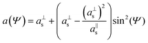 | (3) |
from which the unit cell volume can be determined:When the substrate-supported film is under compressive stress, which is a common feature for sputtered films up to a few hundreds of nm thick,24,27,29,30,32 it is described as “planar stress” (σxx = σyy; σzz = 0). This produces biaxial in-plane strain (uxx = uyy < 0; uzz > 0). Shear component(s) are absent as long as (Y·t)film ≪ (Y·t)sub where Y is Young's modulus and t is thickness, and the subscripts “film” and “sub” denote the film and substrate, respectively. For all thin films described here, the value of (Y·t)film is more than two orders of magnitude smaller than that of (Y·t)sub. Therefore, shear stress components are negligible. The substrate-supported films are under biaxial compression; tensile stress is not present. Partial substrate removal produces a buckled membrane, which is a film tethered to the substrate by its edges. Since the thickness of the film, tf (typically <2 μm), is much smaller than the linear dimension of the membrane (>1 mm), the membrane is free to expand (Fig. 1), relaxing both elastic and, after some time, anelastic strain. For the case of ceria, most of the anelastic strain is relaxed in a few seconds.26 The only remaining strain is limited to the local bending strain:24,33,34| |  | (5) |
where and Rb is the local bending radius (typically ≈ few mm). The magnitude of ub is consequently on the order of 10−4; any resulting changes in lattice vibrational frequencies would be below our detectable limit.33 If the membrane comprises only the film of interest, then the in-plane, a‖m, and out-of-plane, a⊥m, lattice parameters, equilibrate as a‖m = a⊥m = a0, where a0 is the lattice parameter of the strain-free membrane,
The fractional change in volume  is therefore:
| |  | (7) |
If the film is mechanically elastic, then the expected fractional change in volume and of the film vibrational mode frequency, upon film removal from the substrate, should satisfy eqn (1), with the value of γi at constant temperature being close to that of the bulk material under isostatic stress. If the membrane is not a single layer but, for instance, a bilayer, then two scenaria are possible: (i) the mechanical properties of one of the films are dominant, i.e. Yb1·t1 ≫ Yb2·t2,where Yb1, Yb2 are biaxial moduli derived from Young's modulus, Y, and Poisson's ratio, ν, as  and t1,t2 the thicknesses of films 1 and 2. Perturbing effects of the second layer would be negligible, so that for the dominant film, a‖m = a⊥m = a0. This is the case of Gd-doped ceria membranes with an aluminum stress relief layer underneath, as described below. (ii) If, in order to preserve mechanical stability, a two-layer membrane with comparable Yb·t values must be prepared, then for the film of interest, a‖m ≠ a⊥m ≠ a0. This is because comparable Yb·t implies that stress relaxation is incomplete: the films continue to impose stress on each other. Nevertheless, eqn (1)–(6) are still valid. The value of the mode Grüneisen parameter should approximate that for the mechanically elastic, bulk material under isostatic stress as will be shown below for a thin film of Y2O3 deposited on Ti/SiO2/Si. We note that an example has been reported in the literature (ref. 35) of an epitaxial, mechanically elastic film, GaN, for which changes in Raman peak positions as a function of in-plane deposition strain were shown to be comparable to those predicted by the isothermal mode Grüneisen parameter evaluated by isostatic pressure applied to the bulk material.
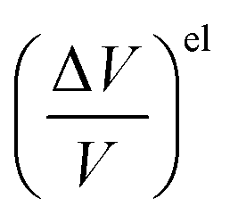
2.2 Separating elastic and anelastic contributions to the fractional volume change
If the film is mechanically anelastic, then the elastic and anelastic components of the in-plane strain of the substrate-supported film can be reliably separated if the membrane is able to achieve a strain-free state: i.e., uxx,m = 0. The in-plane (utotxx) and transverse (utotzz) components of the total strain in the substrate-supported film are:| |  | (8) |
Contributions from both uel,uan are included (eqn (2)). The elastic contribution can be determined if the in-plane stress is isotropic (plane stress), σxx = σyy, and the biaxial modulus Yb of the film material are known:30
| |  | (9) |
where
ν is Poisson's ratio for the film material. The approximation of isotropic biaxial stress is justified. In the vast majority of cases, including this work, special measures are taken to ensure in-plane homogeneity (substrate/source rotation, multiple sources). The value of
σxx can be found
36 from the change in substrate radius of curvature before,
R0, and after film deposition
Rs:
| |  | (10) |
where
Ysub,
tsub and
νsub are Young's modulus, thickness and Poisson's ratio of the substrate. The anelastic component of the in-plane strain is:
| | | uanxx = utotxx− uelxx | (11) |
The volumetric strain for the biaxial case is:
| |  | (12) |
Using the relationship between the in-plane (xx) and out-of-plane (zz) strain in eqn (9), the fractional change in volume due to the elastic component of the total strain can be expressed as:
| | 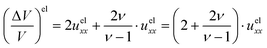 | (13) |
For a membrane that can achieve a strain-free state, a‖m = a⊥m = a0, by measuring the lattice parameters of the film on the substrate, a‖s, a⊥s, the in-plane stress in the substrate supported film σxx = σyy and evaluating a0, it is possible to separate  and
and  .
.
3 Materials and methods
3.1 Thin film fabrication
Three types of GDC thin films were fabricated. 650 nm thick films of (i) 10GDC and (ii) 20GDC were deposited using radio frequency (RF) magnetron sputtering (AJA) from stoichiometric, ceramic targets (Ce0.9Gd0.1O1.95 and Ce0.8Gd0.2O1.9) 99.99% pure, Able targets, Ltd) onto ∼200 nm Al layer, which had been DC sputtered onto a 2” Si wafer (p-Si(100), 0.01 Ω cm, tSi = 280 μm). (iii) ∼500 nm of Ce0.8Gd0.2O1.9 (20GDC-M) was deposited from a metal alloy target (20–80% Gd–Ce alloy target, 99.99% pure, Able targets, Ltd) using RF reactive sputtering on a similar 2-layer Al/Si substrate. Al served as a stress relief layer and the use of both ceramic and metal alloy targets allowed us to determine the influence of target choice on our results. When the ceramic target was used, the GDC layer was deposited under 30 mTorr atmosphere of Ar![[thin space (1/6-em)]](https://www.rsc.org/images/entities/char_2009.gif) :O2, 6:1, while the GDC layer from the metallic target was deposited under 15 mTorr atmosphere of Ar:O2 10:1. During GDC deposition from ceramic or metallic targets, the substrate temperature was 393 K and 273 K, respectively. The samples cooled spontaneously to room temperature under high vacuum inside the deposition chamber. The Al layer also prevented the detection of the Si Raman line at 520.7 cm−1, which interferes with the Raman spectrum of the GDC layer, particularly in the wavenumber region of the ceria F2g mode. An Al mask was deposited on the backside of the Si wafer using DC-sputtering. Using photolithography techniques, 2 mm circular openings were patterned on the Al layer through which the Si layer was subsequently etched via the “Bosch process”,34 creating a self-supported film, i.e. a membrane. Overall, six membranes of 20GDC-M, three membranes of 20GDC and four membranes of 10GDC were fabricated.
:O2, 6:1, while the GDC layer from the metallic target was deposited under 15 mTorr atmosphere of Ar:O2 10:1. During GDC deposition from ceramic or metallic targets, the substrate temperature was 393 K and 273 K, respectively. The samples cooled spontaneously to room temperature under high vacuum inside the deposition chamber. The Al layer also prevented the detection of the Si Raman line at 520.7 cm−1, which interferes with the Raman spectrum of the GDC layer, particularly in the wavenumber region of the ceria F2g mode. An Al mask was deposited on the backside of the Si wafer using DC-sputtering. Using photolithography techniques, 2 mm circular openings were patterned on the Al layer through which the Si layer was subsequently etched via the “Bosch process”,34 creating a self-supported film, i.e. a membrane. Overall, six membranes of 20GDC-M, three membranes of 20GDC and four membranes of 10GDC were fabricated.
Y2O3 thin films were chosen as the “reference” material for two reasons: (i) the cubic phase has double fluorite crystal symmetry and is not known to display anelasticity; consequently, all strain is expected to be purely elastic.37 (ii) Y2O3 has a strong Raman spectral signature. Being mechanically elastic, a Y2O3 film presents a challenge for membrane preparation, as it is unable to absorb the large release of mechanical energy during the membrane fabrication procedure described above. A different approach was therefore required. Amorphous SiO2 (∼1.5 μm thick) was deposited via PECVD on a Si substrate. The temperatures of the bottom and top electrodes during deposition were 473 K and 573 K respectively. The chamber pressure was 1.2 Torr of a N2/N2O gas mixture. Helium was used as a carrying gas with the reactive gas being SiH4. Deposition rate is estimated to be approx. 3 nm per second. SiO2 served as a support layer for the Y2O3 film in order to prevent failure upon substrate removal. A DC-magnetron sputtered, 80 nm thick Ti adhesion layer was then deposited under 5 mTorr pressure Ar, followed by a 430 nm thick RF-magnetron sputtered Y2O3 film (metallic target, 99.99% pure, Able targets, Ltd) in 30 mTorr of 6:1 Ar:O2, substrate temperature 673 K. Passive cooling of the substrate to room temperature was achieved in the deposition chamber in high vacuum, during approximately 1.5 hours. This created a 4-layer stack: Y2O3/Ti/SiO2/Si. Membranes were then prepared as described above; overall, three membranes of Y2O3 were fabricated.
3.2 Structural characterization of substrate-supported thin films and self-supported membranes
X-ray diffraction patterns (XRD, Rigaku TTRAX, Bragg–Brentano, Θ/2Θ; variable divergence slits, scan rate 1 degree min−1) of substrate supported films (S-films), Ce1−xGdxO2−x/2, x = 0.1–0.2 were measured as a function of substrate tilt angle (Ψ). All films were in the fluorite phase. The in- and out-of-plane lattice parameters (a‖s,a⊥s) of the S-films were determined according to eqn (3). (see ESI,† Fig. S1) The lattice parameter of the strain-free GDC membranes, a0, was calculated from the change in the membrane area as determined by a Zeta-20 3D optical profiler according to a procedure described in ref. 24. Scanning electron microscopy (SEM, Zeiss Sigma 500) was used to image the cross-section morphology and thickness of the S-films. In- and out-of-plane lattice parameters of substrate supported Y2O3 films, were also determined according to eqn (3). (see ESI,† Fig. S1) Lattice parameters of self-supported Y2O3 membranes were determined by XRD in reflection and transmission geometries, as described in ref. 19.
3.3 Raman spectroscopy of substrate-supported films and self-supported membranes
Raman spectra of the Gd – doped ceria films were collected with a Horiba LabRam Evolution micro-Raman spectrometer in the back-scattering configuration using a He–Ne excitation laser (632.8 nm, unpolarized), ∼1 μm focal spot-size. Laser power at the sample surface was estimated to be less than 2 mW. Spectra were measured at two locations on both the substrate-supported films and self-supported membranes. Raman spectra of Y2O3 films were measured using a green excitation laser (532 nm, unpolarized), ∼1 μm focal spot-size. Laser power at the sample surface was estimated to be <0.1 mW. Instead of measuring the Raman signal particular spot in the center of the membrane for a prolonged time, sufficient to achieve an acceptable signal to noise ratio, the signal was acquired by scanning of a 10 μm circular diameter (negligibly small with respect to the 2 mm membrane diameter) in order to minimize sample heating and avoid sample degradation. Spectra were measured at four locations, on both the substrate-supported films and self-supported membranes. A 1800 lines per mm grating provided spectral resolution of ∼0.3 cm−1 per pixel. Using Lorentzian profile fitting in MATLAB®, peak position (ω) and linewidth (x) of the well-defined Raman modes were determined. The peak shift was calculated by averaging over membranes and substrate supported films and then subtracting those values. Measurements were completed at least one week following membrane formation, allowing the GDC films sufficient time to achieve a strain-free state.24,26
4 Results and discussion
4.1 Substrate supported thin films vs. self-supported membranes: structure and stability
4.1.1 GDC films and membranes.
As described in Section 3, 650 ± 50 nm thick 10GDC, 20GDC or 500 ± 50 nm thick 20GDC-M films were deposited on a 200 nm thick Al stress relaxation layer on a p(100)-cut Si substrate. The XRD patterns of the GDC films could be indexed according to cubic fluorite (Fm![[3 with combining macron]](https://www.rsc.org/images/entities/char_0033_0304.gif) m) crystallographic symmetry (Fig. 2). 10GDC and 20GDC displayed columnar grain morphology (Fig. 3). SEM cross section images of the 20GDC-M film reveal granular, irregular grain morphology. Comparison of the biaxial Young's modulus of the GDC films relative to the Al layers, shows clear dominance of the former (190 kPa m ≫ 20 kPa m), allowing us to neglect the contribution of the Al layer to the biaxial stress in GDC. The elastic moduli of GDC and Al were taken from ref. 38 and 39 respectively. Using the tilt angle (Ψ) – series of measurements on the as-deposited films and eqn (3), the in-plane, a‖s, and out-of-plane, a⊥s, lattice constants were determined (Fig. 4). All as-deposited films show in-plane compressive strain (a⊥s> a‖s). Partial substrate removal was accomplished using lithography and etching as described in Section 3, giving rise to a 2 mm diameter, self-supported, buckled membrane (Fig. 1). Buckling of the membrane is the result of strain relaxation and associated volume increase of the films.24,34 For the GDC films, stress relaxation was assumed to be complete, as demonstrated in previous work (see ref. 24), and the strain-free lattice parameter, a0, could be determined from the fractional change in membrane area. All GDC films displayed a large anelastic strain component uanxx (see Table 2), which is in agreement with previous reports26–28 of the strong anelasticity observed in doped ceria ceramics. The fractional change in the unit cell volume corresponding to the total strain (ΔV/V)tot and that corresponding to the elastic component of the strain (ΔV/V)el were calculated using eqn (7) and (13) respectively (Tables 1 and 2).
m) crystallographic symmetry (Fig. 2). 10GDC and 20GDC displayed columnar grain morphology (Fig. 3). SEM cross section images of the 20GDC-M film reveal granular, irregular grain morphology. Comparison of the biaxial Young's modulus of the GDC films relative to the Al layers, shows clear dominance of the former (190 kPa m ≫ 20 kPa m), allowing us to neglect the contribution of the Al layer to the biaxial stress in GDC. The elastic moduli of GDC and Al were taken from ref. 38 and 39 respectively. Using the tilt angle (Ψ) – series of measurements on the as-deposited films and eqn (3), the in-plane, a‖s, and out-of-plane, a⊥s, lattice constants were determined (Fig. 4). All as-deposited films show in-plane compressive strain (a⊥s> a‖s). Partial substrate removal was accomplished using lithography and etching as described in Section 3, giving rise to a 2 mm diameter, self-supported, buckled membrane (Fig. 1). Buckling of the membrane is the result of strain relaxation and associated volume increase of the films.24,34 For the GDC films, stress relaxation was assumed to be complete, as demonstrated in previous work (see ref. 24), and the strain-free lattice parameter, a0, could be determined from the fractional change in membrane area. All GDC films displayed a large anelastic strain component uanxx (see Table 2), which is in agreement with previous reports26–28 of the strong anelasticity observed in doped ceria ceramics. The fractional change in the unit cell volume corresponding to the total strain (ΔV/V)tot and that corresponding to the elastic component of the strain (ΔV/V)el were calculated using eqn (7) and (13) respectively (Tables 1 and 2).
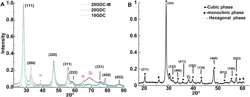 |
| | Fig. 2 XRD patterns measured as described in Section 3, with 3° sample offset: (A) 10GDC, 20GDC, 20GDC-M films. Thin film diffraction peaks are indexed according to Fmm lattice symmetry, while peaks at 38°, 65° are assigned to the Al stress relief layer and the broad peak at 69° to the p-(100)-cut Si substrate; (B) Y2O3 films. Three coexisting phases can be distinguished in the yttria film: the indexed double fluorite phase (Ia) occupies approximately half the sample volume according to quantitative analysis (ESI,† Fig. S2). | |
 |
| | Fig. 3 SEM images of a cross section of 10 mol% Gd doped ceria film deposited as described in Section 3 by RF sputtering from (A) a metal alloy target and (B) a ceramic target on a 200 nm Al stress relief layer on a p(100)-cut Si wafer substrate. (C) Y2O3 film deposited on a Si wafer with intervening Ti and 1.5 μm thick PECVD-deposited SiO2 layers. | |
 |
| | Fig. 4 Lattice parameters of the as-deposited GDC films calculated by X-ray diffraction according to eqn (3) and the strain free parameter a0 of the self-supported membrane calculated by using the optical profilometer as described in Section 3. Standard deviations of a‖s and a⊥s is due to the uncertainty in fitting to eqn (3), while the standard deviation of a0 comes from both replicate measurements (6 membranes of 20GDC-M, 3 membranes of 20GDC and 4 membranes of 10GDC) and measurement accuracy. | |
Table 1 In-plane and out-of-plane lattice parameters of the substrate supported films: a‖s, a⊥s; a0 is the lattice parameter of the strain-free, self-supported GDC membrane.a‖m and a⊥m are the in-plane and out-of-plane lattice parameters of the Y2O3 bilayer membrane; utotxx is the total in-plane strain of the as-deposited GDC film. (ΔV/V)tot is the fractional change in the unit cell volume between the self-supported membrane and the substrate-supported film (the numbers in parentheses designate measurement accuracy)
| Sample |
a
‖s [Å] |
a
⊥s [Å] |
a
0 [Å] |
a
⊥m [Å] |
a
‖m [Å] |
u
tot
xx
[%] |
(ΔV/V)tot |
| 10GDC |
5.441(7) |
5.493(4) |
5.476 (7) |
— |
— |
−0.65(2) |
−0.010(1) |
| 20GDC |
5.45(1) |
5.4885 (6) |
5.476(9) |
— |
— |
−0.43(3) |
−0.006(2) |
| 20GDC-M |
5.4303(4) |
5.4913(2) |
5.459(3) |
— |
— |
−0.52(7) |
−0.005(1) |
| Y2O3 |
10.578(2) |
10.608(1) |
— |
10.580(5) |
10.614(7) |
— |
−0.004(1) |
4.1.2 Y2O3 films and membranes.
As described in Section 3, Y2O3 films were prepared on tri-layer stacks: 80 nm Ti-adhesion layer, 1.5 μm PECVD SiO2, p(100)-cut Si. However, for this sample the value of (Yb·t) for the Y2O3 film and the SiO2 layer (we neglect the small contribution of the 80 nm Ti layer) are comparable, 76 kPa m and 105 kPa m, respectively; consequently, stress relaxation was not complete, as films Y2O3 and SiO2 films continue to impose39 stress on each other. However, the lattice parameter measurements for the Y2O3 films on the substrate and as a membrane are sufficiently precise to enable determination of the fractional volume change required for evaluating the mode Grüneisen parameter corresponding to the total strain. Attempts to achieve full stress relaxation were therefore unnecessary. XRD patterns of the Y2O3 films revealed that they comprise three phases: Ia (cubic, double fluorite), Pm1(hexagonal), C2/m (monoclinic). Quantitative analysis (Jade, MDI) assigned approx. equal fractional sample volume to the cubic (50.7 ± 8.8%) and monoclinic (40.7 ± 7.6%) phases. (see Fig. S2, ESI†). The in-plane stress, as determined by the Stoney formula applied to substrate curvature, is distributed uniformly (i.e. the plane stress case σxx = σyy). Therefore, the grains of the cubic phase all undergo similar changes. Since XRD allows determination of the lattice parameters of a given phase on its own, it is straightforward to trace the changes in unit cell volume of the cubic phase. The cubic lattice parameters of the self-supported Y2O3 membranes are listed in Table 1. (e.g. ref. 19). Following film deposition, the change in wafer curvature was laterally (biaxially) uniform, confirming the presence of in-plane isotropic stress. The values of (ΔV/V)tot and (ΔV/V)el were calculated using eqn (7) and (13), respectively, and found to be compatible (Tables 1 and 2)-justifying the choice of Y2O3 as an elastic reference material.
Table 2 In-plane stress, strain, and the corresponding fractional volume change assigned to each strain component for GDC films upon partial substrate removal. tf,Rf and σxx are the film thickness, the curvature radius of the substrate after film deposition, and the in-plane stress, respectively. uelxx and (ΔV/V)el are the in-plane strain and fractional change in the unit cell volume corresponding to the elastic component of the strain. uanxx is the in-plane strain corresponding to the anelastic component of the strain (the numbers in parentheses designate measurement accuracy). For comparison, Y2O3 is included in the table
| Sample |
t
f (nm) |
R
f (m) |
σ
xx
[MPa] |
u
el
xx
[%] |
u
an
xx
[%] |
(ΔV/V)el |
| 10GDC |
640(30) |
4.6(5) |
720(120) |
−0.24(4) |
−0.41(2) |
−0.0025(4) |
| 20GDC |
660(30) |
6.3(1) |
570(70) |
−0.19(2) |
−0.24(5) |
−0.0022 (4) |
| 20GDCM |
500(50) |
9.3(7) |
510(90) |
−0.17(2) |
−0.36(6) |
−0.0018(2) |
| Y2O3 |
430(50) |
4.8(2) |
520(110) |
0.31(6) |
— |
0.0036(7) |
4.2 Raman spectroscopy of substrate supported films and self-supported membranes
High-resolution Raman spectra of both substrate-supported films and self-supported membranes were acquired for each sample (Fig. 5). A frequency change of 0.8–1.6 cm−1 of the F2g Raman peak from the as-deposited position was measured for the GDC films (Table 3). Three weak, broad, lattice defect-associated bands, centered at 250, 560, 600 cm−1 remained unchanged upon substrate removal. For the as-deposited, substrate supported Y2O3 film, a single, well-defined peak was observed at frequency shift ∼375 cm−1, to which is assigned the Fg Raman active mode40,41 of the cubic phase. An average frequency change of 2.1 cm−1 was measured upon substrate removal, allowing the calculation of the effective mode Grüneisen parameter corresponding to the total strain. As noted in Section 3, the Raman signal was acquired from a 10 μm diameter circular scan in order to avoid sample heating.
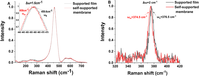 |
| | Fig. 5 Representative, normalized Raman spectra for self-supported membranes and substrate supported films of: (A) 10GDC and (B) Y2O3. A small change in frequency is observed for both the GDC and Y2O3 films of the F2g and Fg modes, respectively, indicative of volume expansion upon substrate removal. In the case of the GDC films, no change could be detected in the defect bands at ∼260, 550 or 600 cm−1. The expanded frequency range for the Y2O3 film is presented in the ESI,† Fig. S3. Given the high spectral resolution of the spectrometer grating (≈0.3 cm−1 per pixel), it is clear that contributions from Raman active-modes of either the monoclinic or hexagonal phases do not interfere with the Fg mode of the cubic phase: the closest vibrational mode due to the monoclinic phase would be the Ag mode at ∼407 cm−1.45,46 | |
Table 3 Change in frequency Δω [cm−1] of the relevant Raman-active mode (F2g for GDC and Fg for Y2O3) observed for the substrate-supported film compared to that observed for the self-supported membrane (see Fig. 5). γtot,γel,γpowder, calculated according to the corresponding volume change, are the mode Grüneisen parameters corresponding to the total strain, elastic component of the strain, and the strain-free powder measured under isostatic stress. The uncertainty in Δω (in parentheses) is determined by averaging over all samples of a given composition
| Sample |
Δω |
γ
total
|
γ
el
|
γ
powder
|
| 10% GDC |
1.6(3) |
0.4(1) |
1.4(4) |
1.4525 |
| 20% GDC |
1.5(3) |
0.5(2) |
1.6(5) |
1.2525 |
| 20% GDCM |
0.8(3) |
0.4(2) |
1.0(5) |
1.2525 |
| Y2O3 |
2.1(4) |
1.4(5) |
|
1.3547 |
4.3 Calculating the effective mode Grüneisen parameter and its significance
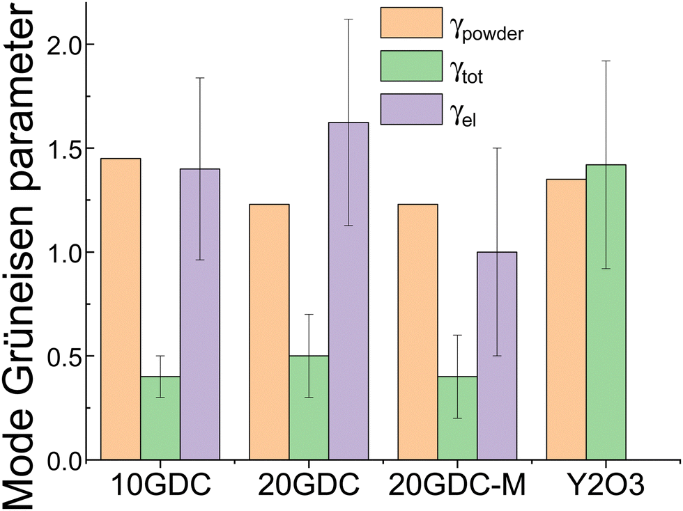
For thin films of Y2O3, a mechanically elastic rare earth oxide (up to 7 GPa pressure where it deforms plastically),37 the Grüneisen parameter of the ∼375 cm−1 Fg mode determined under conditions of anisotropic stress/strain is close to that obtained for the powder under isostatic stress (Fig. 6 and Table 3).42 Considering that similar behavior was reported for GaN films,35 we may suggest that, for elastic materials subject to anisotropic stress, the mode Grüneisen parameter is a valid approximation for change in Raman-active vibrational mode energy, presenting a powerful tool for strain analysis in thin films. However, for Gd-doped ceria films under biaxial compressive deposition stress, the F2g mode Grüneisen parameter, responding to the change in total strain between the in-plane biaxially compressed film and the strain-free, self-supported membrane is only 30–45% of the value calculated for bulk/powder samples under isostatic compression. This agrees with the results of a previous study by Kraynis et al.24 on Raman active F2g mode frequency shifts for Sm- and Eu- doped ceria films. At the same time, the effective mode Grüneisen parameter, corresponding to only the elastic component of the strain, is satisfactorily close to values calculated for trivalent doped ceria powders under isostatic stress.25 The anelastic component of the strain is related to the conversion of mechanical deformation into other forms of energy. For Gd-doped ceria, this is, most probably, the energy of reorienting oxygen vacancy-induced elastic dipoles.31,43 These dipoles are viewed as the source of the anelastic, time dependent response to anisotropic stress observed in doped ceria.44
 |
| | Fig. 6 Comparison of the mode Grüneisen parameter (γtot) calculated for aliovalent doped ceria thin films using eqn (1) and (7); and the effective mode Grüneisen parameter corresponding to the elastic component of the strain (γel) calculated using eqn (1) and (13); γpowder are published values for powder samples under isostatic pressure.25 The mode Grüneisen parameter for cubic Y2O3 (γtot) are, within experimental uncertainty, equivalent to those reported in the literature for powder samples under isostatic pressure.47 Standard deviation was calculated from measurement uncertainty for each membrane and then averaged for all membranes of the same composition. | |
5 Conclusion
The combined experimental/computational protocol presented above is meant to facilitate quantitation and management of anisotropic mechanical stress in devices containing ion-conducting thin films. Using X-ray diffraction and Raman spectroscopy, commonly used nondestructive techniques, we demonstrate a method which allows the calculation of the effective (two-state) mode Grüneisen parameter of thin films by converting them into self-supported membranes. If the material is mechanically elastic, then the membrane will generally require a supporting layer. This study quantitatively substantiates our earlier qualitative suggestion24 that the anelastic component of the total anisotropic strain is responsible for the reduction of the F2g mode Grüneisen parameter measured for the doped ceria film from that measured for bulk/powder samples under isostatic compression. Nevertheless, we show that the change in frequency of the Raman active F2g vibrational mode of sputtered Gd3+ doped ceria films is dominated by a response to the elastic component of in-plane biaxial compressive strain, even though such films generally display anelastic behavior under anisotropic stress. The cubic phase of the mechanically elastic Y2O3 films, analyzed according to the same protocol, displays a change in frequency of the ∼375 cm−1 Fg mode, which is consistent with the response of bulk Y2O3 powders to isostatic stress.
Conflicts of interest
There are no conflicts to declare.
Acknowledgements
This work was supported by the PAZY foundation grant #2018/57. This work made possible in part by the generosity of the Harold Perlman Family and was in part supported by the Minerva Center for Self-Repairing Systems for Energy & Sustainability.
References
- T. S. Stefanik and H. L. Tuller, J. Eur. Ceram. Soc., 2001, 21, 1967 CrossRef CAS.
- D. Beckel, A. Bieberle-Hutter, A. Harvey, A. Infortuna, U. P. Muecke, M. Prestat, J. L. M. Rupp and L. J. Gauckler, J. Power Sources, 2007, 173, 325 CrossRef CAS.
- T. Yu, Z. Ni, C. Du, Y. You, Y. Wang and Z. Shen, J. Phys. Chem. C, 2008, 112, 12602 CrossRef CAS.
- Z. Dohcevic-Mitrovic, M. Scepanovic, M. Grujic-Brojcin, Z. Popovic, S. Boskovic, B. Matovic, M. Zinkevich and F. Aldinger, Solid State Commun., 2006, 137, 387 CrossRef CAS.
- C. Galiotis and D. Batchelder, J. Mater. Sci. Lett., 1988, 7, 545 CrossRef.
- Q. Li, Y. Wang, T. Li, W. Li, F. Wang, A. Janotti, S. Law and T. Gu, ACS Omega, 2020, 5, 8090 CrossRef CAS PubMed.
- I. A. Alhomoudi and G. Newaz, Thin Solid Films, 2009, 517, 4372 CrossRef CAS.
- X. Hu, J. L. Stanford and R. J. Young, Polymer, 1994, 35, 80 CrossRef CAS.
- L. Ma, W. Qiu and X. Fan, Microelectron. Reliab., 2021, 118, 114045 CrossRef CAS.
- R. Schmitt, A. Nenning, O. Kraynis, R. Korobko, A. I. Frenkel, I. Lubomirsky, S. M. Haile and J. L. Rupp, Chem. Soc. Rev., 2020, 49, 554 RSC.
- E. M. Sala, N. Mazzanti, M. B. Mogensen and C. Chatzichristodoulou, Solid State Ionics, 2022, 375, 115833 CrossRef CAS.
- C. Artini, B. Joseph, G. A. Costa and M. Pani, Solid State Ionics, 2018, 320, 152 CrossRef CAS.
- C. Artini, S. Massardo, M. M. Carnasciali, B. Joseph and M. Pani, Energies, 2020, 13 Search PubMed.
- Y. Shi, A. H. Bork, S. Schweiger and J. L. M. Rupp, Nat. Mater., 2015, 14, 721 CrossRef CAS PubMed.
- E. Sediva, D. Bohdanov, G. F. Harrington, I. Rafalovskyi, J. Drahokoupil, F. Borodavka, P. Marton and J. Hlinka, ACS Appl. Mater. Interfaces, 2020, 12, 56251 CrossRef CAS PubMed.
- J. L. M. Rupp, U. P. Muecke, P. C. Nalam and L. J. Gauckler, J. Power Sources, 2010, 195, 2669 CrossRef CAS.
- Y. N. Shi, I. Garbayo, P. Muralt and J. L. M. Rupp, J. Mater. Chem. A, 2017, 5, 3900 RSC.
- H. Li, P. Zhang, G. Li, J. Lu, Q. Wu and Y. Gu, J. Alloys Compd., 2016, 682, 132 CrossRef CAS.
- O. Kraynis, E. Wachtel, I. Lubomirsky and T. Livneh, Scr. Mater., 2017, 137, 123 CrossRef CAS.
- J. McBride, K. Hass, B. Poindexter and W. Weber, J. Appl. Phys., 1994, 76, 2435 CrossRef CAS.
- D. Marrocchelli, S. R. Bishop, H. L. Tuller and B. Yildiz, Adv. Funct. Mater., 2012, 22, 1958 CrossRef CAS.
- C. Artini, M. Pani, M. M. Carnasciali, M. T. Buscaglia, J. R. Plaisier and G. A. Costa, Inorg. Chem., 2015, 54, 4126 CrossRef CAS PubMed.
-
W. H. Weber and R. Merlin, Raman Scattering in Materials Science, Springer Science & Business Media, 2013 Search PubMed.
- O. Kraynis, E. Makagon, E. Mishuk, M. Hartstein, E. Wachtel, I. Lubomirsky and T. Livneh, Adv. Funct. Mater., 2019, 29 Search PubMed.
- F. Iguchi, S. Onodera, N. Sata and H. Yugami, Solid State Ionics, 2012, 225, 99 CrossRef CAS.
- R. Korobko, S. K. Kim, S. Kim, S. R. Cohen, E. Wachtel and I. Lubomirsky, Adv. Funct. Mater., 2013, 23, 6076 CrossRef CAS.
- A. Kossoy, Y. Feldman, R. Korobko, E. Wachtel, I. Lubomirsky and J. Maier, Adv. Funct. Mater., 2009, 19, 634 CrossRef CAS.
- A. Kossoy, A. I. Frenkel, Q. Wang, E. Wachtel and I. Lubomirsky, Adv. Mater., 2010, 22, 1659 CrossRef CAS PubMed.
- N. Goykhman, Y. Feldman, E. Wachtel, A. Yoffe and I. Lubomirsky, J. Electroceram., 2014, 33, 180 CrossRef CAS.
- A. Kossoy, E. Wachtel and I. Lubomirsky, J. Electroceram., 2014, 32, 47 CrossRef CAS.
- R. Korobko, A. Lerner, Y. Li, E. Wachtel, A. I. Frenkel and I. Lubomirsky, Appl. Phys. Lett., 2015, 106, 042904 CrossRef.
- O. Kraynis, I. Lubomirsky and T. Livneh, J. Phys. Chem. C, 2019, 123, 24111 CrossRef CAS.
-
F. Bloom and D. Coffin, Handbook of thin plate buckling and postbuckling, Chapman and Hall/CRC, 2000 Search PubMed.
- E. Mishuk, E. Makagon, E. Wachtel, S. Cohen, R. Popovitz-Biro and I. Lubomirsky, Sens. Actuators, A, 2017, 264, 333 CrossRef CAS.
- C. Kisielowski, J. Krüger, S. Ruvimov, T. Suski, J. Ager III, E. Jones, Z. Liliental-Weber, M. Rubin, E. Weber and M. Bremser, Phys. Rev. B: Condens. Matter Mater. Phys., 1996, 54, 17745 CrossRef CAS PubMed.
- C. A. Klein, J. Appl. Phys., 2000, 88, 5487 CrossRef CAS.
- I. C. Albayrak, S. Basu, A. Sakulich, O. Yeheskel and M. W. Barsoum, J. Am. Ceram. Soc., 2010, 93, 2028 CrossRef CAS.
- N. Yavo, D. Noiman, E. Wachtel, S. Kim, Y. Feldman, I. Lubomirsky and O. Yeheskel, Scr. Mater., 2016, 123, 86 CrossRef CAS.
-
J. E. Hatch, A. Association and A. S. Metals, Aluminum: Properties and Physical Metallurgy, American Society for Metals, 1984 Search PubMed.
- M. V. Abrashev, N. D. Todorov and J. Geshev, J. Appl. Phys., 2014, 116 Search PubMed.
- Y. Repelin, C. Proust, E. Husson and J. Beny, J. Solid State Chem., 1995, 118, 163 CrossRef CAS.
- E. Husson, C. Proust, P. Gillet and J. P. Itie, Mater. Res. Bull., 1999, 34, 2085 CrossRef CAS.
- Y. Li, O. Kraynis, J. Kas, T.-C. Weng, D. Sokaras, R. Zacharowicz, I. Lubomirsky and A. I. Frenkel, AIP Adv., 2016, 6, 055320 CrossRef.
- M. Varenik, S. Cohen, E. Wachtel, A. I. Frenkel, J. C. Nino and I. Lubomirsky, Scr. Mater., 2019, 163, 19 CrossRef CAS.
- Q. Zhang, X. Wu, S. V. Ovsyannikov, J. C. Dong, S. Qin, S. L. Dubrovinsky and D. L. Chen, Chem. Res. Chin. Univ., 2016, 32, 545 CrossRef CAS.
-
S. Deutsch, High pressure phase transformations in polycrystalline yttrium oxide, Rutgers The State University of New Jersey, School of Graduate Studies, 2012 Search PubMed.
- N. D. Sharma, J. Singh, A. Vijay, K. Samanta, S. Dogra and A. K. Bandyopadhyay, J. Phys. Chem. C, 2016, 120, 11679 CrossRef.
Footnotes |
| † Electronic supplementary information (ESI) available. See DOI: https://doi.org/10.1039/d3cp03878e |
| ‡ Present address: Stanford Synchrotron Radiation Lightsource, SLAC National Accelerator Laboratory, Menlo Park, California 94025, USA. |
|
| This journal is © the Owner Societies 2023 |
Click here to see how this site uses Cookies. View our privacy policy here. 
 Open Access Article
 This Open Access Article is licensed under a Creative Commons Attribution-Non Commercial 3.0 Unported Licence
 a,
Olga
Kraynis‡
a,
Olga
Kraynis‡

 where
where  is the fractional change in the vibrational frequency relative to that displayed by the “standard” (i.e., unstrained or minimally strained) material. Eqn (1) provides a basis for assessing lattice strain in bulk materials and, increasingly during the last two decades, in thin films, including the most intensively studied intermediate temperature ion conductors, aliovalent-doped ceria, essential for catalysis, fuel cells and oxygen sensors.1,2,10,11 Indeed, as for bulk ceria,12,13 measurements on thin films report changes in Raman mode frequency that correlate with changes in unit cell dimensions.14–18 The origin and characteristics of anelastic strain in aliovalent-doped ceria thin films have been extensively discussed elsewhere.19


 is therefore:
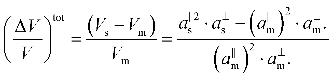
 and t1,t2 the thicknesses of films 1 and 2. Perturbing effects of the second layer would be negligible, so that for the dominant film, a‖m = a⊥m = a0. This is the case of Gd-doped ceria membranes with an aluminum stress relief layer underneath, as described below. (ii) If, in order to preserve mechanical stability, a two-layer membrane with comparable Yb·t values must be prepared, then for the film of interest, a‖m ≠ a⊥m ≠ a0. This is because comparable Yb·t implies that stress relaxation is incomplete: the films continue to impose stress on each other. Nevertheless, eqn (1)–(6) are still valid. The value of the mode Grüneisen parameter should approximate that for the mechanically elastic, bulk material under isostatic stress as will be shown below for a thin film of Y2O3 deposited on Ti/SiO2/Si. We note that an example has been reported in the literature (ref. 35) of an epitaxial, mechanically elastic film, GaN, for which changes in Raman peak positions as a function of in-plane deposition strain were shown to be comparable to those predicted by the isothermal mode Grüneisen parameter evaluated by isostatic pressure applied to the bulk material.


 and
and  .
.