
 Open Access Article
 This Open Access Article is licensed under a
 Creative Commons Attribution 3.0 Unported Licence
Ionic and electronic polarization effects in horizontal hybrid perovskite device structures close to equilibrium†
Davide
Moia
 *,
Mina
Jung
,
Ya-Ru
Wang
and
Joachim
Maier
*,
Mina
Jung
,
Ya-Ru
Wang
and
Joachim
Maier
Max Planck Institute for Solid State Research, Heisenbergstr. 1, 70569, Stuttgart, Germany. E-mail: d.moia@fkf.mpg.de
First published on 5th May 2023
Abstract
The electrical response of hybrid perovskite devices carries a significant signature from mobile ionic defects, pointing to both opportunities and threats when it comes to functionality, performance and stability of these devices. Despite its importance, the interpretation of polarization effects due to the mixed ionic–electronic conducting nature of these materials and the quantification of their ionic conductivities still poses conceptual and practical challenges, even for the equilibrium situation. In this study, we address these questions and investigate the electrical response of horizontal devices based on methylammonium lead iodide (MAPI) close to equilibrium conditions. We discuss the interpretation of DC polarization and impedance spectroscopy measurements in the dark, based on calculated and fitted impedance spectra obtained using equivalent circuit models that account for the mixed conductivity of the perovskite and for the effect of device geometry. Our results show that, for horizontal structures with a gap width between the metal electrodes in the order of tens of microns, the polarization behavior of MAPI is well described by the charging of the mixed conductor/metal interface, suggesting a Debye length in the perovskite close to 1 nm. We highlight a signature in the impedance response at intermediate frequencies, which we assign to ionic diffusion in the plane parallel to the MAPI/contact interface. By comparing the experimental impedance results with calculated spectra for different circuit models, we discuss the potential role of multiple mobile ionic species and rule out a significant contribution from iodine exchange with the gas phase in the electrical response of MAPI close to equilibrium. This study helps to clarify the measurement and interpretation of mixed conductivity and polarization effects in hybrid perovskites with immediate relevance to the characterization and development of transistors, memristors and solar cells based on this class of materials as well as other mixed conductors.
Introduction
Mixed ionic–electronic conduction is a key feature of hybrid halide perovskites.1,2 Particularly, the significant ionic conduction of these compounds at room temperature has been discussed as a challenge in the field of perovskite solar cells, as it greatly affects device reliability and lifetime.3–6 On the other hand, it has also opened new avenues for other applications such as memristive devices.7–9 Developing detailed understanding of ionic transport in these materials is essential to both tackling the device-related issues related to degradation and unstable output, as well as unlocking the full potential derived from the complexity of their properties.10 In particular, knowledge of the defect chemistry of hybrid perovskites can help develop models to decipher their behavior and guide future steps in the design of devices.11–13Most of the reports on mixed conduction in hybrid perovskites have focused on methylammonium lead iodide (MAPI), the most investigated compound of this material class, while recent studies have also explored the role of composition on the ionic properties of other halide perovskites.14–16 These reports have established that MAPI presents p-type electronic conduction in the dark at equilibrium under common preparation conditions. Iodide vacancies are widely considered majority ionic carriers, while other mobile defects have also been discussed.17–20 It was also shown that the stoichiometry of MAPI can be effectively accessed in situ by varying the halogen partial pressure, highlighting the importance of surface reactivity as a channel for component exchange at low temperature.17,21
Although ion transport in hybrid halide perovskite based devices can be suppressed to some extent through compositional engineering, to our knowledge, no composition presenting negligible ion transport at temperatures relevant to the operation of solar cells has been reported to date. Importantly, absence of hysteresis in the current–voltage measurements of hybrid perovskite devices does not imply absence of ion transport. Instead, it can be the result of using scan rates that are either much faster or much slower than the characteristic time scale of ion redistribution.22,23 Even if low hysteresis is observed for a wide range of scan rates, this is still compatible with ion transport if the optoelectronic processes that underlie the solar cell response have negligible dependence on ion redistribution.24–27 Ultimately, a comprehensive analysis of the optoelectronic device response over an extended range of time scales critically relies on understanding how such redistribution occurs.
A complete picture of the mechanism controlling the polarization behavior, that is the long time scale electrochemical response, observed for perovskite devices is still missing. This is the case for the large perturbation regime, relevant to solar cells measured under light,28–30 but even for the simple situation of small perturbation close to equilibrium. Early work on MAPI pellets (symmetrical samples between carbon contacts) showed typical behavior associated with stoichiometric polarization, whereby the long time scale voltage evolution is related to the formation of a gradient in stoichiometry across the bulk of the sample in the direction perpendicular to the MAPI/contact interfaces.1 The kinetics of such polarization is associated with bulk properties, such as the chemical resistance and chemical capacitance of the sample (see also next section). On the other hand, early studies on the capacitance of solar cell devices with variable active layer thickness pointed towards space charge polarization to play an important role, as far as the dynamics of thin films in the 1–100 s time scale is concerned.31 This type of polarization occurs in mixed conducting devices with ion blocking contacts, for which the capacitive response is predominantly associated with changes in mobile ion concentration localized close to the interfaces with the contacts.25–27,32,33 While both stoichiometric and interfacial polarization effects are expected in solar cells based on hybrid perovskites, the relevant parameter ranges in which either or both of these processes dominate the response need to be clarified. To complicate this picture, other factors such as electrochemical reactions with electrodes and iodine evolution,34–36 ionic penetration in the contacts,37 the role of multiple mobile ions19,20 have also been invoked in the literature to explain the behavior of hybrid perovskite devices under even relatively low bias. Finally, the observation of multiple low frequency features in impedance spectra highlights a complex capacitive and in some cases inductive behavior that still awaits clarification.26,38,39
In this study, we investigate the electrical response of MAPI based devices with horizontal structure in the dark. This architecture is common in the fabrication of field-effect-transistors and memristors, and it is used here to achieve careful control of device properties. By elucidating the role of active layer and contact geometry in the measured polarization time constant and in the observed features of impedance spectra, we show that charging of the perovskite/metal interface is the dominating polarization mechanism in these architectures under small perturbation and close to equilibrium. Finally, we explore the role of exchange reactions with the gas phase and of multiple mobile ions through equivalent circuit calculations, and we discuss implications for the horizontal devices investigated here as well as for solar cells.
Background
The electrical response of mixed ionic–electronic conductors (MIECs) involves transport, reaction and storage of ionic and electronic charge carriers. This wide range of processes typically implies a complex dependence on the time scale (or frequency) at which the response is evaluated, also depending on the sample properties (e.g. MAPI between ion-blocking contacts, Fig. 1). The behavior of MIECs is described analytically through the Nernst–Planck–Poisson model (NPP, also referred to as drift-diffusion),40–42 and it can be conveniently represented in terms of equivalent circuit elements. In this section, we review some fundamental concepts of equivalent circuit modeling of MIECs close to equilibrium, which will be referred to in the discussion of the data in this study. For further reading on this subject, see ref. 41–44. | ||
| Fig. 1 Schematics showing the processes responsible for the electrical response of a mixed ionic–electronic conductor, such as methylammonium lead iodide (MAPI), of thickness L between ion-blocking contacts and close to equilibrium. Two electronic and two ionic charge carriers are shown (the superscripts ˙ and ′ indicates a positively and a negatively charged defect relative to the perfect crystal). The charge transport and storage behavior of the device depends on the frequency of the applied bias. The separation of processes occurring at either “low” or “high” frequencies depends on the specific properties of the device. Note that the two ions can have very different diffusion coefficients. | ||
The transmission line model encapsulates the NPP equations in an electrical circuit in one-dimension (x). Specifically, the model is a representation of the linearized NPP problem and can be used to study the small perturbation behavior of semiconducting and MIEC based devices close to equilibrium. The circuit involves one rail for each mobile charge carrier (electronic or ionic) consisting of electrochemical resistors Rj(xi) = σj−1(xi)Δx/A (for the j-th charge carrier) connected along the x dimension (Fig. 2a). Here, σj(xi) is the conductivity of the carrier within the slice of MIEC with thickness Δx = xi+1 − xi and area A. The potential associated with the nodes on each charge carrier's rail in the transmission line corresponds to the species’ electrochemical potential ![[small mu, Greek, tilde]](https://www.rsc.org/images/entities/i_char_e0e0.gif) j, more precisely to its deviation, dj (indicated with vj in Fig. 2a, qvj = dj, q is the elementary charge), from the equilibrium value, j,eq (j = j,eq + dj). An additional rail describing the electrostatic behavior of the system involves electrostatic capacitors,
j, more precisely to its deviation, dj (indicated with vj in Fig. 2a, qvj = dj, q is the elementary charge), from the equilibrium value, j,eq (j = j,eq + dj). An additional rail describing the electrostatic behavior of the system involves electrostatic capacitors,  , also connected along x (
 indicates the static dielectric permittivity of the MIEC). If ϕ = ϕeq + dϕ is the electrostatic potential expressed as its equilibrium value and its deviation from equilibrium, then the potential at the nodes of the electrostatic rail corresponds to the changes in the electrostatic potential dϕ, here indicated with ve. Each charge carrier rail is connected to the electrostatic rail via chemical capacitors (Fig. 2a, right side) defined as:
 | (1) |
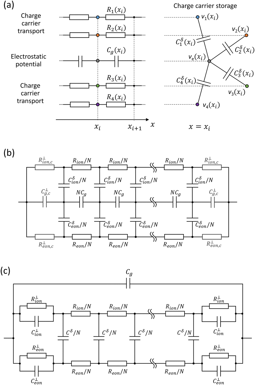 | ||
| Fig. 2 Transmission line models for mixed ionic–electronic conductors close to equilibrium in the dark. (a) Constituting parts of the transmission line model for the case of four mobile charge carriers: (left) charge carrier transport rails (electrochemical resistors) and electrostatic rail (electrostatic capacitors) along the position axis, x; (right) charge carrier storage implemented through chemical capacitors (e.g. Cjδ(xi) for the j-th charge carrier) connected between the nodes of each charge carrier rail (here displayed for x = xi) and the electrostatic rail. The potentials vj refers to the change in electrochemical potential of the j-th charge carrier (qvj = dj, q is the elementary charge), while ve is the change in electrostatic potential (ve = dϕ). (b) Transmission line circuit model for two charge carriers (the subscripts eon and ion refer to electronic and ionic). Resistors and capacitors modeling the interfacial contribution due to the contacts are also included (R⊥eon,c, R⊥eon,c and C⊥g,c). (c) Approximated version of circuit (b): the electrostatic rail is replaced by a single capacitor, and the electronic and ionic chemical capacitors in the bulk are combined. The elements R⊥eon, R⊥ion, C⊥eon and C⊥ion describe the interfacial behavior associated with each charge carrier. | ||
Under dilute conditions, we can write:
 | (2) |
In general for MIECs, we are interested in the transport of mobile point defects such as conduction band electrons (e′ with concentration n), valence band holes (h˙ with concentration p) and any kind of ionic species. Under the conditions that are relevant to this study, where ion-blocking, non-selective (with respect to electrons and holes) contacts are used and measurements are carried out close to equilibrium, the electron and hole populations are expected to be at equilibrium locally. This means that a single rail can be used to summarize the electronic behavior of the MIEC (see Fig. 2b). Such approximation would not be valid in general (e.g. solar cell architecture with selective contacts), and especially for the characterization of the electrical response out-of-equilibrium.25,26,46–49 In Fig. 2b, the total electronic resistance and the total electronic chemical capacitance are Reon and Cδeon, respectively. The local contribution of a Δx thick slice of the MIEC to these electronic properties is shown as Reon/N and Cδeon/N, assuming a discretized model with equal spacing (N is the number of mesh points, assumed to be large) and the simple case of homogeneous MIEC. Ionic species are described analogously. In Fig. 2b, we consider one mobile ionic charge carrier with a total transport resistance Rion and ionic chemical capacitance Cδion. The role of multiple ions (multiple ionic rails) and chemical equilibria (additional elements connecting ionic and electronic rails) will be addressed below.
In Fig. 2b, the contribution of the boundary layers on the MIEC side are treated similarly to the bulk. Interfacial contributions due to the contacts are described via interfacial resistors and capacitors R⊥ion,c, R⊥eon,c, C⊥g,c. Their values determine the reversibility of the electrodes to each species (ability to enable, small R⊥, or to block, large R⊥, the exchange of charge carriers with the contact) and describe the interfacial electrostatic situation (if the contact is a metal, C⊥g,c is a double layer capacitance). While accurate, the impedance of the circuit in Fig. 2b has no simple analytical form. A commonly used approximation to such model is the circuit shown Fig. 2c.38,42 Here, the chemical capacitors related to electronic and ionic species in the bulk of the MIEC are combined into a chemical capacitance Cδ, as (Cδ)−1 = (Cδion)−1 + (Cδeon)−1, which refers to the storage of the relevant component (e.g. iodine in MAPI). As transport of such component involves both electronic and ionic transport, the chemical resistance Rδ = Reon + Rion is also defined. The geometric capacitance Cg encapsulates the contributions of the whole electrostatic rail of circuit 2b. The interfacial behavior is described by the elements R⊥eon, R⊥ion, C⊥eon, C⊥ion.41,44 If the double layer capacitance C⊥g,c is large, Cj⊥ represents the space charge capacitance at the interface associated with the j-th charge carrier:
 | (3) |
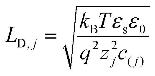 is the corresponding Debye length.34 Importantly, Cj⊥ is independent on MIEC thickness, L, as opposed to Cjδ, which is linearly proportional to L.
Let us consider a situation where contacts show ion-blocking and ohmic behavior, and where cion ≫ ceon (relevant to this study). It follows that R⊥ion → ∞, R⊥eon → 0 and C⊥ion ≫ C⊥eon. In addition, if χeon ≈ 1, then the chemical capacitance can be approximated as Cδ ≈ Cδeon and its value can be very small in the dark. The impedance Z (normalized by A) for the transmission line model in Fig. 2b resulting from such condition is shown with red data points in Fig. 3a for the frequency range ƒ = 10−5–104 Hz (inset in Fig. 3a displays the corresponding capacitance, calculated as C = Im[Z−1](2πƒ)−1). The data are compared with the calculated impedance obtained when considering a small value of χeon, shown with cyan data points. This refers to the case of significant trapping of electronic charge carriers, which results in large Cδeon, and therefore in large Cδ.1
 | ||
| Fig. 3 (a) Nyquist plot of calculated impedance spectra for a MIEC between ion blocking contacts, R⊥ion → ∞ (angular frequency ω = 2πƒ, with f being the frequency). Two input parameter sets are considered where the value of the ionic chemical capacitance is fixed and the value of the electronic chemical capacitance is either Cδeon ∼3 × 10⁻²Cδion, giving rise to a large Cδ, or Cδeon ∼3 × 10⁻¹¹Cδion, giving rise to a small Cδ. All other parameters have the same value (see Methods). The low-frequency behavior can be described in terms of (small Cδ) space charge polarization or (large Cδ) stoichiometric polarization. The inset in (a) shows ω−1 Im[Z−1] (capacitance of the system for close to equilibrium conditions) plotted vs. frequency. (b) and (c) illustrate the equivalent circuits that describe the low frequency behaviors for the two situations. | ||
At high frequency, the impedance in the Nyquist plot forms practically identical semi-circles for the two examples. Such feature is related to the parallel of the ionic and electronic resistances and the overall sample's geometric capacitance Cg. On the other hand, the features associated with the low frequency behavior show a pronounced difference in terms of spectral shape and in the time constant depending on the value of Cδ. The low frequency semicircle for the case of small Cδ can be well explained by the circuit in Fig. 3b, where the blocking of the ions by the contacts gives rise to the space charge polarization behavior.44 For the large Cδ data, the polarization gives rise to a Warburg feature (initial increase in impedance at 45° on the Nyquist plot for decreasing frequency), characteristic of ambipolar diffusion. Such feature derives from the dynamics of stoichiometry gradient build-up across the bulk of the sample (see also energy level description13 and further discussion in Fig. S1, ESI†).
While both space charge polarization and stoichiometric polarization processes inevitably occur in all MIEC based systems with ion-blocking contacts, only one of the two processes generally dominates the low frequency response. As a result, the low frequency capacitance corresponds to about C⊥ion/2 or ∼Cδ/12 (see inset of Fig. 3a), with a time constant in the order of (Reon + Rion)C⊥ion/2 = RδC⊥ion/2 and ∼RδCδ/12, respectively (assuming R⊥eon ≪ Reon).44,50 The 1/2 and 1/12 terms account for the series of the two space charge capacitors and for the fact that the chemical capacitors are charged to different fractions of the applied voltage and through different networks of resistors depending on their position in the circuit, respectively. It follows that, for a MIEC between metal contacts, the low frequency capacitance is typically ≤10−4 F cm−2 (depending on the charge carrier concentration and corresponding Debye length) and it is independent on sample thickness for cases where space charge polarization is dominant. On the other hand, it has no upper limit and it is linearly proportional to the sample thickness for cases where the buildup of a stoichiometric gradient in the MIEC is the rate limiting process to the polarization. The scaling of the capacitive response at low frequency with device thickness can be used as a discriminating factor to evaluate the regime under which a MIEC based system is operating. We will use this argument to discuss our results below.
Results and discussion
A. Electrical response of MAPI based horizontal devices
Electrical measurements of MAPI based horizontal devices were conducted in the dark at 40 °C in controlled atmosphere (see Methods section and ref. 14 and 51). The device structure is displayed in Fig. 4a and b, highlighting the two geometrical parameters, L and LC, that we explored in the results discussed below. Fig. 4c and d show the DC Galvanostatic polarization and impedance spectroscopy measurements performed on one such device. | ||
| Fig. 4 Electrical characterization of MAPI based horizontal devices. (a) Schematics showing the cross section of the device with the two geometric parameters controlled in this study: L is the distance between the electrodes and LC is the width of the electrode fingers. (b) Schematics of top view of the interdigitated contacts with total overlap of W (Nf is the total number of fingers). (c) DC Galvanostatic polarization and (d) impedance spectroscopy measurements performed on a device with L = 10 μm, LC = 5 μm and W = 24.83 cm in argon atmosphere, in the dark and at 40 °C. In (c), a constant voltage baseline (∼0.5 mV) was subtracted from the data. Polarization behavior displayed (e) vs. the square root of time and (f) on a semi logarithmic plot. The orange data points in (f) are obtained by using a smoothed version of the measured voltage data to calculate (Vf − V)/V and are used for the fit to extract the time constant τ (Vf stands for the asymptotic value of the voltage during the polarization). | ||
The DC measurement indicates an increase in the measured voltage with time (t) on application of a constant current to the sample. The measurement allows us to analyze the polarization occurring in the thousands of seconds time scale (τ ∼ 1500 s, Fig. 4f) and extract the long time scale value of the conductivity. Based on the assumption of ion-blocking contacts, such value can be assigned to the electronic component only (in this case σeon = 3.4 × 10⁻¹⁰ S cm−1).1 The early time scale behavior of the DC polarization plotted vs the square root of time (Fig. 4e) highlights the initial voltage jump on application of the current, which can be assigned to the total conductivity (ionic and electronic contributions) of the sample. It also displays a trend of the voltage vs. t1/2 that appears approximately linear for the early times. The latter feature is typical of a diffusion process and potentially consistent with a Warburg-like low frequency feature in impedance terms. This consideration may point towards stoichiometric polarization dominating the response of the sample.
However, when looking at the impedance response, which allows us to analyze the high and intermediate frequency region (fast and intermediate time scales) more carefully, a different picture arises. At frequencies > 1 Hz, a semicircle in the Nyquist plot can be attributed to the (high frequency) total resistance and geometric capacitance of the device. At lower frequencies, instead of a Warburg feature, we observe a slightly depressed semicircle-like feature. While the response of the sample according to the profile of the DC measurement in Fig. 4e appears as a diffusion process, the low frequency feature of the impedance spectrum indicates a less straightforward behavior. We also observe a relatively small mid-frequency region (frequencies ∼0.1–1 Hz) separating the low frequency polarization from the high frequency semicircle. Importantly, the method to extract the correct value of the total resistance (conductivity) depends on the nature of this mid-frequency feature, as highlighted with red arrows in the inset of Fig. 4d. Such value might also differ from the one extracted by using the initial jump in the DC measurement as a measure of the total resistance times the current (red arrow in the inset of Fig. 4e). Indeed, the time scale associated with this estimate is dependent on the time resolution of the instrument used (see Section 2 in the ESI†). In order to investigate the nature of these features and to ascertain the role of space charge polarization and stoichiometric polarization in the observed response, we studied devices with systematically varied geometry. With reference to Fig. 4a, we fabricated samples where the values of gap width between the contact fingers, L, and the finger width, LC, were varied over almost one order of magnitude (between 5–40 μm).
Fig. 5a and b show the DC polarization (normalized data) obtained for devices with variable L and LC, respectively. The data indicate an increase in the time constant describing the long time scale behavior when either parameter is increased (Fig. S4, ESI†). The electronic conductivity extracted from the measurements, shown in Fig. 5c as function of L or LC depending on the experiment, is generally reproducible for the different devices, with only a slight increase when increasing the value of L. This trend could be interpreted by considering a finite value of R⊥eon associated with the MAPI/Au interface. The nature of this resistance may be due to some injection barrier at the interface or to a more complex space charge situation forming in MAPI at the interface with gold and with the alumina substrate (see analysis in Fig. S5, ESI†).52Fig. 5c also displays the ionic conductivity, which was extracted by first evaluating the total conductivity (σtot) from the high frequency semicircle of the impedance spectra (see discussion below and Fig. S3, ESI†) and evaluating σion = σtot − σeon. As discussed above, the dependence of τ/Rδ on L can provide useful information on the dominant polarization process in these devices. The relatively constant profile of such dataset plotted against the gap width L, displayed in Fig. 5d, suggests that the capacitive component responsible for the polarization is independent of the active layer thickness and is probably of interfacial nature. We find that the dependence of τ/Rδ on LC is instead approximately linear, indicating that the increase in finger width effectively increases the capacitance involved in the long time scale polarization.
 | ||
| Fig. 5 DC galvanostatic polarization measurements of MAPI deposited on horizontal devices with interdigitated gold contacts. Data for devices with gap width between the contacts and contact finger width in the range 5–40 μm are shown. Normalized voltage measurement upon application of a current step at time = 0 (for all measurements the voltage was <60 mV) showing (a) the gap width L and (b) the finger width LC dependence of the polarization behavior. The current was applied for a variable time depending on the device. (c) Electronic and ionic conductivities extracted from the measurements in (a) and (b) (impedance measurements were also used in the analysis, see text). (d) Long time scale capacitive behavior of the devices evaluated from the analysis of the time constant extracted from the data in (a) and (b) divided by the chemical resistance Rδ = Reon + Rion. | ||
Further insights into the electrical response of the devices is gathered from the analysis of their impedance spectra, displayed in Fig. 6c and Fig. 6d. The trend in the high frequency feature in Fig. 6c indicates the increase of the total resistance following the increase in the value of L. On the other hand, Fig. 6d shows an approximately unvaried high frequency feature for different LC, but a striking change in the mid-frequency behavior. The region with data points arranged with approximately ∼45° slope increases in size when increasing the value of LC.
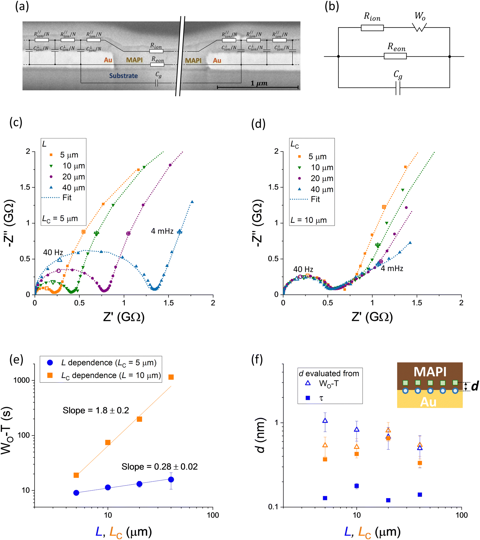 | ||
| Fig. 6 Impedance measurements on MAPI based devices with horizontal architecture and interdigitated gold contacts (same as Fig. 4). (a) and (b) Extended and compact equivalent circuit model fitted to the experimental data (see discussion in text). The circuit in (a) is superimposed to a cross-sectional SEM image of a device. Impedance spectra measured for devices with (c) variable gap width L and (d) variable finger width LC. The dotted lines are fits obtained using the circuit in (b). The empty symbols and the crossed empty symbols indicate the complex impedance of the samples measured at 40 Hz and 4 mHz, respectively. (e) Dependence of the WO-T parameter describing the finite Warburg element (associated with the mid-frequency behavior of the impedance) on L and LC. (f) Effective distance d between the charges at the metal/MAPI interface, extracted from either WO-T or τ. We assign the value of d to the Debye length in MAPI. | ||
To interpret this observation, we consider the device geometry and the approximate paths that are taken by ionic and electronic charge carriers. In the region between the contacts, we expect ionic and electronic charges (holes are the relevant carriers here53) to be transported within the bulk of the halide perovskite. Based on the discussion of Fig. 5, the transport in this region can be modeled with a simplified version of the transmission line circuit in Fig. 2c, where the bulk chemical capacitance is omitted (Fig. 6a). Once the charges reach the gold contact, electronic carriers find a low resistance path while ions are blocked at such interface. The charging of the gold contacts, which gives rise to the observed polarization, occurs via charging of the Au/MAPI interface with electronic charges on the gold side and ionic charges on the MAPI side. For the latter to occur, ionic defects need to diffuse in the direction parallel to the MAPI/Au interface over a distance (LC/2, given the symmetry of the interdigitated contacts) that is comparable to the gap between the contacts for this sample geometry. This ion diffusion gives rise to the mid-frequency feature in the impedance spectra. The behavior is analogous to the charge diffusion observed in electrolytes penetrating porous conductive electrodes, as discussed by de Levie.54 This interpretation is confirmed by the change in the size of the mid-frequency transition relative to the overall impedance for the L dependent data. Such intermediate region almost disappears, in relative terms, for the device with the longest gap width (L = 40 μm). Indeed, in this case the width of the contact is significantly shorter than L.
Based on the observed trends, a simplified way to model the two-dimensional problem at the MAPI/Au interface is to consider a one-dimensional transmission line, where the electronic resistance on the metal side is practically zero and the ionic resistance of the layer on top of the contact (R‖ion)) is related to the ionic conductivity in MAPI (Fig. 6a). The capacitance C⊥ion is, in this case, a distributed contact capacitance and its meaning is associated with both the chemical and the electrostatic components of the interfacial charging at each position.55 By “condensing” such transmission line model within an open Warburg element (WO), we derive the equivalent circuit in Fig. 6b. The result of fitting such model to the data is displayed in Fig. 6c and d (see dotted lines), from which we obtain the value of Rion, used to evaluate the ionic conductivity displayed in Fig. 5c. Note that, based on the equivalent circuit model in Fig. 6b, the total conductivity can be extracted from the high frequency semicircle without accounting for the mid-frequency feature (see Fig. 3d). We also emphasize the dependence of the parameter WO-T, which is the time constant associated with the Warburg element, on L and LC. This fitted parameter scales approximately with the square of LC, as expected for a diffusion process, while it is much less sensitive to variations in L (Fig. 6e). The complete set of fitting results is shown in Fig. S6 (ESI†).
As a consistency check, we can use two methods to extract the value of the effective distance d between the electronic and ionic charges in the gold and in MAPI, respectively, on charging. A first method involves evaluating such distance from the value of capacitance observed for the DC polarization measurement (τ/Rδ). Alternatively, we can use the parameter WO-T and extract d based on the ionic diffusion in the MAPI region on top of the metal contact (see Methods section for more details).56 The results are displayed in Fig. 6f and show distances in the range of 0.1–1 nm, if one assumes a relative dielectric permittivity of this region of 32.1 These values correspond to specific capacitance values of the electrode/MAPI interfaces as high as 20–200 μF cm−2. The results interpreted in terms of space charge polarization in MAPI (assuming very large capacitance for the gold contact and the core separating MAPI and the metal) imply a value of the Debye length (λ) in the order of 1 nm and a charging mechanism that effectively occurs over the first ionic layer(s) (the iodide ionic radius is ∼0.21 nm). This estimate of λ is roughly consistent with our previous estimate obtained from the analysis of ionically-generated space charges between MAPI and metal oxides,52 and points towards ionic defect concentrations in MAPI in the order of 1019 cm−3 (mobility ∼10−9 cm−2 V−1 s−1).
B. Effects of multiple mobile ionic species and halogen exchange with the gas phase
We explore other possible effects that can contribute to the observed electrical response of hybrid perovskite devices close to equilibrium by performing impedance spectra calculations of one dimensional transmission line equivalent circuit models (Fig. 7a). First, we describe the exchange of iodine with the gas phase. Based on the equilibrium reaction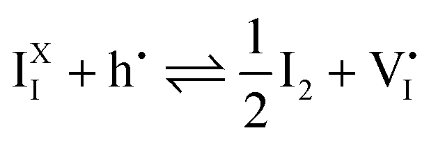 , fixing the iodine partial pressure P(I2) in the gas phase corresponds, in equivalent circuit model terms, to applying a potential difference between the electronic and the (iodide) ionic rails via an impedance element Zexc. The latter describes the exchange reaction kinetics at the solid/gas interface.55 Because we are interested in the small signal behavior of the circuit, only Zexc contributes to the impedance calculation.
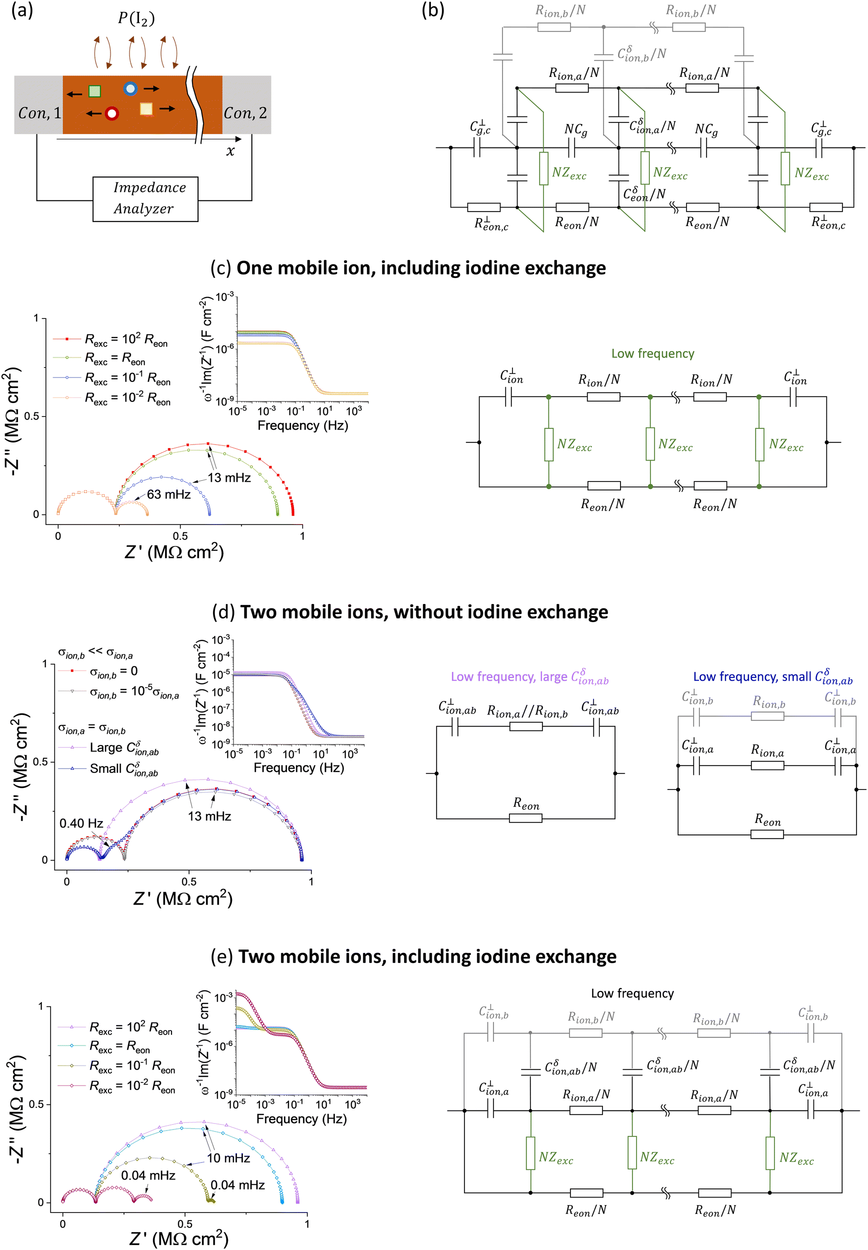 | ||
| Fig. 7 Calculated transmission line impedance considering the effect of the number of mobile ionic species and component (e.g. iodine) exchange with the gas phase. (a) Schematics showing the relevant processes. (b) Complete circuit model for the system in (a) in the dark. In all the simplified examples (c–e), the case where the chemical capacitance between the electronic and ionic rail does not contribute significantly to the low frequency response is considered. The circuit models describing the low frequency behavior for each situation is shown on the right. | ||
Second, we consider the description of two ionic species, indicated with a and b (e.g. transport of iodide and methylammonium defects in MAPI).19,20 Following the transmission line approach in Fig. 2, we include two ionic rails of resistance Rion,a and Rion,b that are connected to the electrostatic rail via chemical capacitors Cδion,a and Cδion,b. If the ionic disorder reaction between the two defects establishes local equilibrium at a fast enough rate compared to the ionic transport through the device, a single ionic rail can be used, where the total ionic resistance is  and the total ionic chemical capacitance is Cδion = Cδion,a + Cδion,b (see Fig. S7 in the ESI†). In this case, the circuit reduces again to the one in Fig. 2b. Below we explore the situation where ionic disorder is not at equilibrium (at the time scale of the impedance analysis), and therefore two separate rails for the two ions are needed. Fig. 7b shows the resulting circuit model including two ionic species (not at equilibrium) and the component exchange impedance. In the discussion that follows, we further simplify this circuit by focusing on its approximated versions at low frequencies, for different situations (see also analytical treatment in Section 6 of the ESI†). We also neglect the chemical capacitance between electronic and ionic charges in the system (see Fig. 5 and 6 and discussion above) and consider negligible values for the interfacial electronic resistance R⊥eon,c.
Fig. 7c considers the effect of component exchange for the one mobile ion case. Because the NZexc elements connect the electronic and ionic rails, ionic conduction can contribute to the low frequency conductivity despite the ion blocking properties of the contacts, as evidenced by the impedance data (here Zexc is assumed to be a resistor Zexc = Rexc). When Rexc < Reon, the size of the semicircle associated with the low frequency impedance reduces. For very low values of Rexc, the ionic and electronic rails are essentially connected in parallel and the electrical response tends to a purely resistive behavior (see also the decrease in the low frequency capacitance for decreasing Rexc). The low frequency response can be described with the equivalent circuit model in Fig. 7c. For the case of MAPI based devices, we can interpret this result as follows: while the application of an electrical bias would establish a gradient in iodine chemical potential in the sample (along the x direction), the fixed P(I2) in the gas phase eliminates such gradient for low enough values of Rexc. As a result, the DC response of the system involves, in addition to the steady state flow of electronic charges in MAPI, a flow of iodide defects as well as an equal and opposite flow of iodine  in the opposite direction in the gas phase. Importantly, the electronic conductivity in the sample could be overestimated when associating the very low frequency (or very long time scale) resistance with Reon, without accounting for the contribution from Rexc. Secondly, because the high frequency semicircle resistance remains unchanged on varying the value of Rexc, the extracted ionic conductivity can, on the other hand, be underestimated when using the formula σion = σtot − σeon.
Next, we consider the situation where two mobile ionic defects (a and b) are at play. We define the chemical capacitance describing the storage of ab (e.g. MAI in MAPI) for ions that are not at equilibrium based on (Cδion,ab)−1 = (Cδion,a)−1 + (Cδion,b)−1. If the ionic concentration of a and b is large, the value of Cδion,ab can be significant, implying that the two ionic rails shown in Fig. 7b are effectively in parallel in the relevant frequency range. A single ionic rail can then be used, as shown in the left circuit in Fig. 7d (note that the interfacial capacitance C⊥ion,ab is calculated referring to the Debye length that includes contributions from both ions). If σion,b ≪ σion,a, the contribution of b to the impedance is negligible, although a slight variation in the shape of the low frequency feature is observed compared with the σion,b = 0 case. More significant changes occur if the two ions contribute to σion to a similar extent (here we consider σion,a = σion,b). In the Nyquist plot in Fig. 7d, the pink data points (large Cδion,ab) refer to such situation, assuming the same ionic concentration and mobilities for the two defects as for the one ionic defect in the reference case (red data points). Compared with the case of a single mobile ion, a smaller high frequency semicircle (lower ionic resistance) and a larger capacitance at low frequencies (shorter Debye length) are observed for the two mobile ion case. Another interesting scenario occurs if σion,a = σion,b, but at least one of the two ionic defects is low in concentration, resulting in a low value of Cδion,ab. This implies that the rails associated with the two ions can no longer be considered in parallel for the evaluation of the low frequency polarization, as shown in the right circuit of Fig. 7d. As an example, we consider b to have four orders of magnitude lower concentration and four order of magnitude higher mobility than a. The blue data points in Fig. 7d show that two features appear at low frequencies. The difference in the time constants associated with the two features is due to the different values for the interfacial capacitors for each ionic rail, which are related to each ionic defect concentration as discussed above (Rion,aC⊥ion,a/2 ≠ Rion,bC⊥ion,b/2).
Finally, we consider the two effects discussed in Fig. 7c and d occurring simultaneously. In Fig. 7e, two mobile ionic species (e.g., iodide and MA vacancies) with equal value of mobility and concentration (large Cδion,ab case) and different values of Rexc are considered. The exchange with the gas phase effectively allows for a constant flux of one of the ionic species at steady state but not of the other. As a result, a stoichiometric polarization involving the two ionic defects is established at low frequencies. In our example, a gradient in the chemical potential of MAI is generated across the active layer thickness (along x), its formation dominating the very low frequency response of the sample. As evident from the calculated impedance, an additional (Warburg) feature at low frequencies arises for low enough values of Rexc, which is attributed to stoichiometric polarization. The capacitance associated with such feature (see inset in Fig. 7d) can become larger than the capacitance related to the series of the interfacial capacitors, approaching Cδion,ab/12 as discussed for Fig. 3.
We now discuss whether these effects can be relevant for measurements of mixed conduction in hybrid perovskite devices in the dark, in relation to the experiments performed on MAPI presented in this study. The effect of iodine exchange on the measured impedance can be tested by comparing samples with and without encapsulation. An insulating layer on top of the perovskite is expected to significantly increase the value of Zexc. In Fig. 8a, we show that the electrical response and conductivities obtained from such analysis for measurements in argon are comparable. This suggests that the kinetics of component excorporation in argon is not critical to the evaluation of the partial conductivities in MAPI under these conditions. However, the contribution of Zexc to the measured electrical response may become important when the sample is investigated under a fixed P(I2). The P(I2) dependence of the ionic and electronic conductivities for a MAPI sample, extracted as described above, are plotted in Fig. 8b. We observe a relatively unvaried ionic conductivity (value similar to the one measured under argon) over about two orders of magnitude change in P(I2) and an increase in the electronic conductivity that follows approximately σeon ∝ P(I2)0.5. The trend was the same irrespective of device geometry (see Fig. S9 and S10, ESI†) and is consistent with previous reports from our group and others.17,21 The results confirm the p-type electronic conduction within the intrinsic regime.53 Furthermore, we can rule out a dominant contribution of the iodine exchange with the gas phase as an “alternative path” for the measured electrical conduction at low frequencies close to equilibrium. Indeed, this path involves the flow of ionic charges in the device, which is limited by the ionic conductivity of MAPI, as illustrated in Fig. 7c. Because the data in Fig. 8b show that σeon > σion at large enough P(I2), they confirm that conduction at low frequencies is dominated by electronic transport in the active layer. As a consequence, the impedance spectra associated with devices measured at high P(I2) can be analyzed using the circuit model in Fig. 6b, as shown in Fig. 8c. The data show that the larger the P(I2), the more the electronic conductivity dominates the impedance response, with the low frequency feature associated with the space charge polarization shrinking in magnitude. No significant changes are observed in the capacitance spectra when varying P(I2) (inset of Fig. 8c). The results are consistent with the space charge capacitance dominating the low frequency response and the approximately unvaried ionic defect concentration (and Debye length) expected when varying stoichiometry within the intrinsic region of MAPI.53
 | ||
| Fig. 8 Electrical measurements on MAPI based horizontal devices with LC = 5 μm and L = 10 μm performed in the dark close to equilibrium. (a) Comparison of impedance spectra and conductivities for devices with and without a PMMA encapsulation layer coated on top of the MAPI film (measurements performed in argon). Iodine partial pressure dependence of (b) the ionic and electronic conductivities, (c) the impedance spectra and (inset) capacitance of a MAPI device without encapsulation (the capacitance is expressed in F cm−1 as it is normalized by W only). The empty symbols in (b) are measurements performed at the end of the experiment to check for reversibility. | ||
Finally, we cannot rule out a significant contribution coming from the transport of two different ionic species to the observed electrical response of the devices. This is however unlikely, in that the mobility of MA and Pb defects have been established to be much lower than that for iodide.17 The role of protons may be relevant for devices prepared and/or measured under humid atmosphere, which was not the case for our experiments.57 We conclude by pointing out that other effects, such as a second ionic species that is lower in concentration but higher in mobility (see Fig. 7d), as well as grain boundary contributions, could also explain the presence of the mid-frequency feature observed in our impedance measurements. However, the device geometry trend presented in this study clearly assigns such feature to the diffusion of mobile ions in MAPI on top of the metal electrodes. In Section 8 of the ESI,† we discuss how the interpretation described above should be modified in presence of significant grain boundary resistance, which may be relevant to other halide perovskite compositions or preparation protocols.
In terms of implications for design and characterization of hybrid perovskite devices, the results presented in this study indicate that, for application relevant thicknesses (value of L in the horizontal devices investigated here), space charge polarization determines the dynamics of ionic redistribution and electric field screening in MAPI based devices close to equilibrium.58,59 This work also outlines a self-consistent approach for the study of mixed ionic–electronic conductivity in thin films using horizontal architectures. These structures enable the investigation of mixed-conducting properties of thin films within devices with well-defined geometry. The bottom contact structure used here (electrodes fabricated on substrate before active layer deposition) enables direct contact of the perovskite layer with metal electrodes, allowing one to analyze the active layer's behavior without significant interfacial space charge influence from the electrode side. A similar approach can be implemented in vertical structures too,60 provided that no metal penetration in the active layer occurs during metal deposition. Transferring such analysis to conventional solar cell device structures with vertical architecture presents a number of challenges, including control of active layer thickness homogeneity and ion interactions (penetration, reaction) with the contacts, and should be addressed in the future. We note that the importance of device geometry, including two dimensional effects, can become relevant to vertical devices with rough and/or inhomogeneous interfaces, potentially introducing additional mid-frequency features associated with slow ion motion in these areas. The use of contact materials other than metals, including organic and inorganic semiconductors, can complicate the analysis due to the presence of significant space charges not only in the perovskite, but also on the contact side of the interfaces. These effects originate from electronic and, importantly, also from ionic equilibration (adsorption or exchange).52,61 The latter process can potentially introduce slow dynamics in the observed response on electrical biasing. The investigation of ionic conductivity and polarization effects close to equilibrium is therefore an important basic characterization step for these devices, enabling the identification of the processes dominating their dynamic behavior as function of the solar cell's parameters.
Conclusions
We performed a systematic electrical characterization of mixed ionic–electronic conductivity in methylammonium lead iodide devices with horizontal structures. The data show that charging of the metal contact/MAPI interface dominates the long time scale response in the dark close to equilibrium of devices with effective thickness (gap width between contacts) up to tens of microns. This confirms that space charge polarization is the relevant low frequency process for devices with relatively thin active layers (or channel length) such as solar cells and transistors, when measured close to equilibrium and close to room temperature. The data suggest ionic charging at the contact/MAPI interface occurring via ion diffusion on top of the contact and in direction parallel to such interface, a feature relevant to horizontal devices with the structure considered in this study. We estimate a Debye length of ∼1 nm width, suggesting a large (∼1019 cm−3) mobile ionic defect concentration. We could also conclude that, when evaluating conductivities in these systems, information from DC measurements and also from impedance spectroscopy are necessary to accurately establish the contribution of the different components at different time scales (frequencies). Our analysis emphasizes the importance of accounting for sample geometry and presents a simple equivalent circuit model that can be used to investigate partial conductivities in devices with horizontal structures. Finally, from the impedance calculations presented, we highlight possible influence of multiple mobile ionic species and of iodine exchange with the gas phase affecting the estimation of the electronic and ionic conductivities, and we rule out significant contribution from the latter effect in the analysis performed on MAPI under the conditions explored in this work. Our study provides a framework to evaluate mixed ionic–electronic conduction in hybrid perovskites close to equilibrium, an important step towards the analysis of the more complex device response under bias.Methods
Sample fabrication and characterization
Thin films of MAPI were deposited on alumina substrates with interdigitated electrodes using a previously reported procedure.51,52 The MAPI precursor solution consisted of 1.5 M MAI and 1.5 M PbI2 dissolved in DMSO. The film processing was performed through spin coating and by using the anti-solvent method (chlorobenzene was used). The films were annealed at 100 °C for 5 minutes. The thickness of the films was determined via cross-sectional SEM, performed at the end of the experiments (see Fig. S12, ESI†). The electrodes on the substrate were patterned using a photo-lithography process and involved 20 nm of chromium used as an adhesion layer and 200 nm of gold. For both the L and the LC dependent studies, the four devices shared the same substrate, meaning that a single MAPI film was used for each investigation. This approach enabled more careful analysis of the geometrical effects compared with similar experiments performed on separate substrates with different electrode geometries. For conductivity measurements, the samples were loaded in a measuring cell which enabled control of the sample temperature, the environmental conditions and electrical connection to the sample. Measurements were performed at 40 °C, and under argon gas flow (O2 concentration <30 ppm) or under fixed iodine partial pressure using argon as carrier gas. DC polarization measurements were performed using a Keithley source meter, while AC impedance was performed using a Novocontrol spectrometer. The displayed data were obtained after letting the sample stabilize at any given condition. Under argon, small changes in the long time scale behavior were still present between measurements after more than one week of continuous measurements (as expected for the case of P(I2) not being fixed). Such changes occurred at a time scale that was slower than the measured polarization. We measured samples using X-ray diffraction (Panalytical Empyrean (Cu Kα, λ = 0.154 nm)) in Bragg–Brentano and grazing-incident geometry in a gas-tight dome to prevent exposure to air. Measurements performed before and after the electrical characterization showed negligible degradation of the perovskite (see Fig. S13, ESI†).Data analysis
From the relevant resistances (e.g. Rion) extracted from electrical measurements, we evaluated the corresponding conductivity using the relation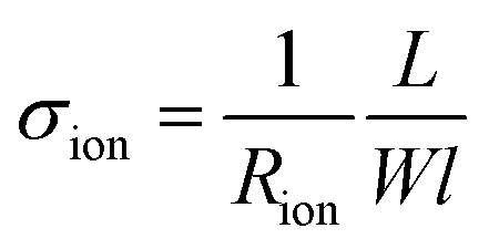 , where l is the thickness of the MAPI layer between the gold contacts (a value of 200 nm was considered, see Fig. 6a and Fig. S12, ESI†). Fitting of equivalent circuit models to the impedance data was performed using Z-view. For DC polarization measurements, a linear function was fitted to the data (see Fig. 4f) in a semilogarithmic plot. For some datasets, the single exponential fitting yielded slightly different results for the time constant and for the asymptotic value of the polarization voltage, depending on the initial time chosen for the fitting range. For simplicity, a single exponential function was used in all cases. The value of the initial time for the fit was increased until the fitting parameter associated with the asymptotic voltage value Vf yielded an approximately linear profile for the function (Vf − V)/Vf at long time scales. The final time for the fitting was chosen such that the fitted data (Vf − V)/Vf (before smoothing) in the fitted range were predominantly positive (negative values would yield imaginary logarithm values and would affect the accuracy of the fitting). We note that very slow stoichiometric polarization processes (due to slower ionic defects) may be occurring and giving rise to the dispersive polarization observed in some of the measurements (slightly depressed semicircle in Fig. 4d and 7d for the σion,b ≪ σion,a case). The values of d displayed in Fig. 6f were extracted based on two methods as discussed in the text. The first method involves considering an effective distance associated with the capacitive term displayed in Fig. 5d,
  (ε0 is the dielectric permittivity of vacuum, while the dielectric permittivity of MAPI
  was assumed to be 321). The factor (WO-R/2) is included here to account for the additional ionic resistance of the MAPI region on top of the gold contact (for the data measured in argon and shown in Fig. 6 this value is negligible compared to Rδ, such that
  ). The second method involves the parameter WO-T, for which we can write
  according to the analysis of the kinetics of space charge storage for the case of dual-phase transport.56 Here l// is the thickness of MAPI on top of the gold contact (we assumed l// = (200 ± 50) nm, see Fig. 6a and Fig. S12, ESI†). We note that stoichiometric effects leading to the stretched behavior discussed above could also lead to some overestimation of the time constant due to interfacial charging evaluated from DC polarization. This could partially explain the discrepancy in the values of d calculated from τ compared to the ones calculated from WO-T.
Impedance spectra calculations
The calculations were performed using a MATLAB code that evaluates the impedance of a given equivalent circuit model by solving a system of equations, each representing Kirchhoff's current law at all nodes minus one. Values for the electronic and ionic transport and charge storage parameters were explored based on literature values and to evaluate the role of different possible polarization behaviors. These values are listed in Section 11 of the ESI.† By using the model in Fig. 2b as a starting point, additional components have been investigated (e.g. two mobile ions, equilibrium with gas phase) as described in the Results section and in Fig. 7. The mesh for the calculations involved a finer spacing close to the boundaries and was refined based on an a posteriori error estimation. Accuracy in the order of 0.5% is estimated for all calculations with the following method. First, the numerical problem is solved with a fine mesh, yielding a reference solution for the impedance Zref. The calculation is run for other three meshes with much coarser spacing (by a factor of 5, 10 and 20). The error associated with the latter solutions with respect to the reference solution is calculated as averaged over the frequency range considered (10−5–104 Hz). From a linear fit in double logarithmic scale of the error vs the number of mesh points, the estimated number of mesh points needed to obtain an error with respect to the reference solution below the set tolerance, Tol, is calculated. Based on the slope of the error vs the number of points (αErr), one can estimate the actual error for the optimized number of points as Tol/(1 − (Nopt/Nref)αErr). A minimum ration Nopt/Nref = 1/4 is guaranteed by the code. If the resulting mesh is coarser than such factor, the solution is calculated. Conversely, another reference solution is calculated based on a mesh that is at least 4 times finer than the one defined by Nopt. The iteration stops when the above mentioned condition is met. The same protocol is applied to both the number of points associated with the interfacial regions and with the bulk. Typical values of the total number of nodes and of the number of interfacial points amounted to N = 500 and Nint = 10–200 (depending on the value of the circuit elements considered).
Conflicts of interest
There are no conflicts of interest to declare.Acknowledgements
We thank Achim Güth, Marion Hagel and Ulrike Waizmann (Nanostructuring Lab in the Max Planck Institute for Solid State Research, Jürgen Weis’ group) for preparation of patterned substrates and for cross-sectional SEM measurements, Dr Helga Hoier for guidance in the XRD characterization, Florian Kaiser for technical assistance. We also thank Dr Rotraut Merkle for useful feedback on this manuscript. DM is grateful to the Alexander von Humboldt Foundation for financial support. Open Access funding provided by the Max Planck Society.References
- T. Y. Yang, G. Gregori, N. Pellet, M. Grätzel and J. Maier, The Significance of Ion Conduction in a Hybrid Organic-Inorganic Lead-Iodide-Based Perovskite Photosensitizer, Angew. Chem., Int. Ed., 2015, 54, 7905–7910 CrossRef CAS PubMed.
- C. Eames, J. M. Frost, P. R. F. Barnes, B. C. O’Regan, A. Walsh and M. S. Islam, Ionic transport in hybrid lead iodide perovskite solar cells, Nat. Commun., 2015, 6, 2–9 Search PubMed.
- M. Ghasemi, B. Guo, K. Darabi, T. Wang, K. Wang, C. Huang, B. M. Lefler, L. Taussig, M. Chauhan, G. Baucom, T. Kim, E. D. Gomez, J. M. Atkin, S. Priya and A. Amassian, A multiscale ion diffusion framework sheds light on the diffusion – stability – hysteresis nexus in metal halide perovskites, Nat. Mater., 2023, 22, 329–337 CrossRef CAS PubMed.
- D. A. Jacobs, C. M. Wolff, X. Y. Chin, K. Artuk, C. Ballif and Q. Jeangros, Lateral ion migration accelerates degradation in halide perovskite devices, Energy Environ. Sci., 2022, 15, 5324–5339 RSC.
- J. Thiesbrummel, V. M. Le Corre, F. Peña-Camargo, L. Perdigón-Toro, F. Lang, F. Yang, M. Grischek, E. Gutierrez-Partida, J. Warby, M. D. Farrar, S. Mahesh, P. Caprioglio, S. Albrecht, D. Neher, H. J. Snaith and M. Stolterfoht, Universal Current Losses in Perovskite Solar Cells Due to Mobile Ions, Adv. Energy Mater., 2021, 11, 1–10 Search PubMed.
- S. P. Dunfield, L. Bliss, F. Zhang, J. M. Luther, K. Zhu, M. F. A. M. van Hest, M. O. Reese and J. J. Berry, From Defects to Degradation: A Mechanistic Understanding of Degradation in Perovskite Solar Cell Devices and Modules, Adv. Energy Mater., 2020, 10, 1–35 Search PubMed.
- Z. Xiao and J. Huang, Energy-Efficient Hybrid Perovskite Memristors and Synaptic Devices, Adv. Electron. Mater., 2016, 2, 1–8 Search PubMed.
- X. Zhao, H. Xu, Z. Wang, Y. Lin and Y. Liu, Memristors with organic–inorganic halide perovskites, InfoMat, 2019, 1, 183–210 CrossRef CAS.
- W. Tress, Metal Halide Perovskites as Mixed Electronic-Ionic Conductors: Challenges and Opportunities – From Hysteresis to Memristivity, J. Phys. Chem. Lett., 2017, 8, 3106–3114 CrossRef CAS PubMed.
- L. Schmidt-Mende, V. Dyakonov, S. Olthof, F. Ünlü, K. M. T. Lê, S. Mathur, A. D. Karabanov, D. C. Lupascu, L. M. Herz, A. Hinderhofer, F. Schreiber, A. Chernikov, D. A. Egger, O. Shargaieva, C. Cocchi, E. Unger, M. Saliba, M. M. Byranvand, M. Kroll, F. Nehm, K. Leo, A. Redinger, J. Höcker, T. Kirchartz, J. Warby, E. Gutierrez-Partida, D. Neher, M. Stolterfoht, U. Würfel, M. Unmüssig, J. Herterich, C. Baretzky, J. Mohanraj, M. Thelakkat, C. Maheu, W. Jaegermann, T. Mayer, J. Rieger, T. Fauster, D. Niesner, F. Yang, S. Albrecht, T. Riedl, A. Fakharuddin, M. Vasilopoulou, Y. Vaynzof, D. Moia, J. Maier, M. Franckevičius, V. Gulbinas, R. A. Kerner, L. Zhao, B. P. Rand, N. Glück, T. Bein, F. Matteocci, L. A. Castriotta, A. Di Carlo, M. Scheffler and C. Draxl, Roadmap on organic-inorganic hybrid perovskite semiconductors and devices, APL Mater., 2021, 9, 1–82 Search PubMed.
- A. Senocrate and J. Maier, Solid-State Ionics of Hybrid Halide Perovskites, J. Am. Chem. Soc., 2019, 141, 8382–8396 CrossRef CAS PubMed.
- D. Moia and J. Maier, Ion Transport, Defect Chemistry, and the Device Physics of Hybrid Perovskite Solar Cells, ACS Energy Lett., 2021, 6, 1566–1576 CrossRef CAS.
- D. Moia and J. Maier, Ionic and electronic energy diagrams for hybrid perovskite solar cells, Mater. Horiz., 2023 10.1039/d2mh01569b.
- G. Y. Kim, A. Senocrate, Y. R. Wang, D. Moia and J. Maier, Photo-Effect on Ion Transport in Mixed Cation and Halide Perovskites and Implications for Photo-Demixing, Angew. Chem., Int. Ed., 2021, 60, 820–826 CrossRef CAS PubMed.
- R. Garcia-Rodriguez, D. Ferdani, S. Pering, P. J. Baker and P. J. Cameron, Influence of bromide content on iodide migration in inverted MAPb(I1-xBrx)3 perovskite solar cells, J. Mater. Chem. A, 2019, 7, 22604–22614 RSC.
- D. W. Ferdani, S. R. Pering, D. Ghosh, P. Kubiak, A. B. Walker, S. E. Lewis, A. L. Johnson, P. J. Baker, M. S. Islam and P. J. Cameron, Partial cation substitution reduces iodide ion transport in lead iodide perovskite solar cells, Energy Environ. Sci., 2019, 12, 2264–2272 RSC.
- A. Senocrate, I. Moudrakovski, G. Y. Kim, T.-Y. Yang, G. Gregori, M. Grätzel and J. Maier, The Nature of Ion Conduction in Methylammonium Lead Iodide: A Multimethod Approach, Angew. Chem., Int. Ed., 2017, 56, 7755–7759 CrossRef CAS PubMed.
- D. Barboni and R. A. De Souza, The thermodynamics and kinetics of iodine vacancies in the hybrid perovskite methylammonium lead iodide, Energy Environ. Sci., 2018, 11, 3266–3274 RSC.
- Y. Liu, N. Borodinov, L. Collins, M. Ahmadi, S. V. Kalinin, O. S. Ovchinnikova and A. V. Ievlev, Role of Decomposition Product Ions in Hysteretic Behavior of Metal Halide Perovskite, ACS Nano, 2021, 15, 9017–9026 CrossRef CAS PubMed.
- Y. Yuan and J. Huang, Ion Migration in Organometal Trihalide Perovskite and Its Impact on Photovoltaic Efficiency and Stability, Acc. Chem. Res., 2016, 49, 286–293 CrossRef CAS PubMed.
- N. Leupold, A. L. Seibel, R. Moos and F. Panzer, Electrical Conductivity of Halide Perovskites Follows Expectations from Classical Defect Chemistry, Eur. J. Inorg. Chem., 2021, 2882–2889 CrossRef CAS.
- R. García-Rodríguez, A. J. Riquelme, M. Cowley, K. Valadez-Villalobos, G. Oskam, L. J. Bennett, M. J. Wolf, L. Contreras-Bernal, P. J. Cameron, A. B. Walker and J. A. Anta, Inverted Hysteresis in n–i–p and p–i–n Perovskite Solar Cells, Energy Technol., 2022, 10, 2200507 CrossRef.
- V. M. Le Corre, J. Diekmann, F. Peña-Camargo, J. Thiesbrummel, N. Tokmoldin, E. Gutierrez-Partida, K. P. Peters, L. Perdigón-Toro, M. H. Futscher, F. Lang, J. Warby, H. J. Snaith, D. Neher and M. Stolterfoht, Quantification of Efficiency Losses Due to Mobile Ions in Perovskite Solar Cells via Fast Hysteresis Measurements, Sol. RRL, 2022, 6, 2100772 CrossRef CAS.
- P. Calado, A. M. Telford, D. Bryant, X. Li, J. Nelson, B. C. O’Regan and P. R. F. Barnes, Evidence for ion migration in hybrid perovskite solar cells with minimal hysteresis, Nat. Commun., 2016, 7, 1–10 Search PubMed.
- D. Moia, I. Gelmetti, M. Stringer, O. Game, D. Lidzey, E. Palomares, P. Calado, J. Nelson, W. Fisher and P. R. F. Barnes, Ionic-to-electronic current amplification in hybrid perovskite solar cells: ionically gated transistor- interface circuit model explains hysteresis and impedance of mixed conducting devices, Energy Environ. Sci., 2019, 12, 1296–1308 RSC.
- A. Pockett, G. E. Eperon, N. Sakai, H. J. Snaith, L. M. Peter and P. J. Cameron, Microseconds, milliseconds and seconds: Deconvoluting the dynamic behaviour of planar perovskite solar cells, Phys. Chem. Chem. Phys., 2017, 19, 5959–5970 RSC.
- D. A. Jacobs, Y. Wu, H. Shen, C. Barugkin, F. J. Beck, T. P. White, K. Weber and K. R. Catchpole, Hysteresis phenomena in perovskite solar cells: The many and varied effects of ionic accumulation, Phys. Chem. Chem. Phys., 2017, 19, 3094–3103 RSC.
- H. J. Snaith, A. Abate, J. M. Ball, G. E. Eperon, T. Leijtens, N. Noel, S. D. Stranks, J. T. W. Wang, K. Wojciechowski and W. Zhang, Anomalous Hysteresis in Perovskite Solar Cells, J. Phys. Chem. Lett., 2014, 5, 1511–1515 CrossRef CAS PubMed.
- K. Domanski, B. Roose, T. Matsui, M. Saliba, S. H. Turren-Cruz, J. P. Correa-Baena, C. R. Carmona, G. Richardson, J. M. Foster, F. De Angelis, J. M. Ball, A. Petrozza, N. Mine, M. K. Nazeeruddin, W. Tress, M. Grätzel, U. Steiner, A. Hagfeldt and A. Abate, Migration of cations induces reversible performance losses over day/night cycling in perovskite solar cells, Energy Environ. Sci., 2017, 10, 604–613 RSC.
- S. E. J. O’Kane, G. Richardson, A. Pockett, R. G. Niemann, J. M. Cave, N. Sakai, G. E. Eperon, H. J. Snaith, J. M. Foster, P. J. Cameron and A. B. Walker, Measurement and modelling of dark current decay transients in perovskite solar cells, J. Mater. Chem. C, 2017, 5, 452–462 RSC.
- O. Almora, I. Zarazua, E. Mas-marza, I. Mora-sero, J. Bisquert and G. Garcia-belmonte, Capacitive Dark Currents, Hysteresis, and Electrode Polarization in Lead Halide Perovskite Solar Cells, J. Phys. Chem. Lett., 2015, 1645–1652 CrossRef CAS PubMed.
- L. Bertoluzzi, C. C. Boyd, N. Rolston, J. Xu, R. Prasanna, B. C. O’Regan and M. D. McGehee, Mobile Ion Concentration Measurement and Open-Access Band Diagram Simulation Platform for Halide Perovskite Solar Cells, Joule, 2020, 4, 109–127 CrossRef CAS.
- N. E. Courtier, M. Cave, J. M. Foster, A. B. Walker and G. Richardson, How transport layer properties affect perovskite solar cell performance: insights from a coupled charge transport/ion migration model, Energy Environ. Sci., 2019, 12, 396–409 RSC.
- R. A. Kerner, P. Schulz, J. A. Christians, S. P. Dunfield, B. Dou, L. Zhao, G. Teeter, J. J. Berry and B. P. Rand, Reactions at noble metal contacts with methylammonium lead triiodide perovskites: Role of underpotential deposition and electrochemistry, APL Mater., 2019, 7, 1–10 Search PubMed.
- L. Zhao, R. A. Kerner, Z. Xiao, Y. L. Lin, K. M. Lee, J. Schwartz and B. P. Rand, Redox Chemistry Dominates the Degradation and Decomposition of Metal Halide Perovskite Optoelectronic Devices, ACS Energy Lett., 2016, 1, 595–602 CrossRef CAS.
- R. A. Kerner and B. P. Rand, Linking Chemistry at the TiO2/CH3NH3PbI3 Interface to Current-Voltage Hysteresis, J. Phys. Chem. Lett., 2017, 8, 2298–2303 CrossRef CAS PubMed.
- R. A. Kerner, S. Heo, K. Roh, K. MacMillan, B. W. Larson and B. P. Rand, Organic Hole Transport Material Ionization Potential Dictates Diffusion Kinetics of Iodine Species in Halide Perovskite Devices, ACS Energy Lett., 2021, 6, 501–508 CrossRef CAS.
- E. Ghahremanirad, S. Olyaee and J. Bisquert, Inductive Loop in the Impedance Response of Perovskite Solar Cells Explained by Surface Polarization Model, J. Phys. Chem. Lett., 2017, 1402–1406 CrossRef CAS PubMed.
- S. Ravishankar, O. Almora, C. Echeverría-Arrondo, E. Ghahremanirad, C. Aranda, A. Guerrero, F. Fabregat-Santiago, A. Zaban, G. Garcia-Belmonte and J. Bisquert, Surface Polarization Model for the Dynamic Hysteresis of Perovskite Solar Cells, J. Phys. Chem. Lett., 2017, 8, 915–921 CrossRef CAS PubMed.
- T. R. Brumlev and R. P. Buck, Transmission line equivalent circuit models for electrochemical impedances, J. Electroanal. Chem., 1981, 126, 73–104 CrossRef.
- J. Jamnik and J. Maier, Generalised equivalent circuits for mass and charge transport: chemical capacitance and its implications, Phys. Chem. Chem. Phys., 2001, 3, 1668–1678 RSC.
- W. Lai and S. M. Haile, Impedance spectroscopy as a tool for chemical and electrochemical analysis of mixed conductors: A case study of ceria, J. Am. Ceram. Soc., 2005, 88, 2979–2997 CrossRef CAS.
- J. Maier, Physical Chemistry of Ionic Materials, Wiley-VCH Verlag GmbH & Co. KGaA, 2005 Search PubMed.
- J. Jamnik and J. Maier, Treatment of the Impedance of Mixed Conductors Equivalent Circuit Model and Explicit Approximate Solutions, J. Electrochem. Soc., 1999, 146, 4183 CrossRef CAS.
- J. Maier, Mass Transport in the Presence of Internal Defect Reactions - concept of conservative ensembles: I, Chemical Diffusion in Pure Compounds, J. Am. Ceram. Soc., 1993, 76, 1218–1222 CrossRef CAS.
- A. J. Riquelme, K. Valadez-Villalobos, P. P. Boix, G. Oskam, I. Mora-Seró and J. A. Anta, Understanding equivalent circuits in perovskite solar cells. Insights from drift-diffusion simulation, Phys. Chem. Chem. Phys., 2022, 24, 15657–15671 RSC.
- L. J. Bennett, A. J. Riquelme, J. A. Anta, N. E. Courtier and G. Richardson, Avoiding Ionic Interference in Computing the Ideality Factor for Perovskite Solar Cells and an Analytical Theory of Their Impedance-Spectroscopy Response, Phys. Rev. Appl., 2023, 19, 1 Search PubMed.
- H. Wang, A. Guerrero, A. Bou, A. M. Al-Mayouf and J. Bisquert, Kinetic and material properties of interfaces governing slow response and long timescale phenomena in perovskite solar cells, Energy Environ. Sci., 2019, 12, 2054–2079 RSC.
- M. Fischer, D. Kiermasch, L. Gil-Escrig, H. J. Bolink, V. Dyakonov and K. Tvingstedt, Assigning ionic properties in perovskite solar cells; a unifying transient simulation/experimental study, Sustain, Energy Fuels, 2021, 5, 3578–3587 CAS.
- J. Jamnik, J. Maier and S. Pejovnik, Powerful electrical network model for the impedance of mixed conductors, Electrochim. Acta, 1999, 44, 4139–4145 CrossRef CAS.
- G. Y. Kim, A. Senocrate, T. Yang, G. Gregori, M. Grätzel and J. Maier, Large tunable photoeffect on ion conduction in halide perovskites and implications for photodecomposition, Nat. Mater., 2018, 17, 445–450 CrossRef CAS PubMed.
- G. Y. Kim, A. Senocrate, D. Moia and J. Maier, Ionically Generated Built-In Equilibrium Space Charge Zones—a Paradigm Change for Lead Halide Perovskite Interfaces, Adv. Funct. Mater., 2020, 30, 1–9 Search PubMed.
- A. Senocrate, T. Y. Yang, G. Gregori, G. Y. Kim, M. Grätzel and J. Maier, Charge carrier chemistry in methylammonium lead iodide, Solid State Ionics, 2018, 321, 69–74 CrossRef CAS.
- R. de Levie, On porous electrodes in electrolyte solutions-IV, Electrochim. Acta, 1964, 9, 1231–1245 CrossRef CAS.
- J. Jamnik and J. Maier, Generalised equivalent circuits for mass and charge transport: chemical cpacitances and its implications, Phys. Chem. Chem. Phys., 2001, 3, 1668–1678 RSC.
- C. C. Chen, E. Navickas, J. Fleig and J. Maier, Kinetics of Space Charge Storage in Composites, Adv. Funct. Mater., 2018, 28, 1–11 Search PubMed.
- D. R. Ceratti, A. Zohar, R. Kozlov, H. Dong, G. Uraltsev, O. Girshevitz, I. Pinkas, L. Avram, G. Hodes and D. Cahen, Eppur si Muove: Proton Diffusion in Halide Perovskite Single Crystals, Adv. Mater., 2020, 32, 1–12 CrossRef PubMed.
- S. A. L. Weber, I. M. Hermes, S. H. Turren-Cruz, C. Gort, V. W. Bergmann, L. Gilson, A. Hagfeldt, M. Graetzel, W. Tress and R. Berger, How the formation of interfacial charge causes hysteresis in perovskite solar cells, Energy Environ. Sci., 2018, 11, 2404–2413 RSC.
- D. Moia, I. Gelmetti, P. Calado, Y. Hu, X. Li, P. Docampo, J. de Mello, J. Maier, J. Nelson and P. R. F. Barnes, Dynamics of internal electric field screening in hybrid perovskite solar cells probed using electroabsorption, Phys. Rev. Appl., 2022, 10, 1 Search PubMed.
- C. Xu, M. S. Alvar, G.-J. A. H. Wetzelaer and P. W. M. Blom, Analysis of the ionic and dielectric properties of perovskites by impedance spectroscopy, J. Appl. Phys., 2023, 133, 045501 CrossRef CAS.
- J. Maier, Nanoionics: Ion transport and electrochemical storage in confined systems, Nat. Mater., 2005, 4, 805–815 CrossRef CAS PubMed.
Footnote |
| † Electronic supplementary information (ESI) available. See DOI: https://doi.org/10.1039/d3cp01182h |
| This journal is © the Owner Societies 2023 |