
 Open Access Article
 This Open Access Article is licensed under a
 Creative Commons Attribution 3.0 Unported Licence
Laser-induced tuning of graphene field-effect transistors for pH sensing†
Aku
Lampinen
 a,
Erich
See
a,
Aleksei
Emelianov
a,
Pasi
Myllyperkiö
a,
Andreas
Johansson
ab and
Mika
Pettersson
*a
a,
Erich
See
a,
Aleksei
Emelianov
a,
Pasi
Myllyperkiö
a,
Andreas
Johansson
ab and
Mika
Pettersson
*a
aNanoscience centre, Department of Chemistry, University of Jyväskylä, Survontie 9, Jyväskylä 40500, Finland. E-mail: mika.j.pettersson@jyu.fi
bNanoscience centre, Department of Physics, University of Jyväskylä, Survontie 9, Jyväskylä 40500, Finland
First published on 29th March 2023
Abstract
Here we demonstrate, using pulsed femtosecond laser-induced two-photon oxidation (2PO), a novel method of locally tuning the sensitivity of solution gated graphene field-effect transistors (GFETs) without sacrificing the integrity of the carbon network of chemical vapor deposition (CVD) grown graphene. The achieved sensitivity with 2PO was (25 ± 2) mV pH−1 in BIS-TRIS propane HCl (BTPH) buffer solution, when the oxidation level corresponded to the Raman peak intensity ratio I(D)/I(G) of 3.58. Sensitivity of non-oxidized, residual PMMA contaminated GFETs was 20–22 mV pH−1. The sensitivity decreased initially by 2PO to (19 ± 2) mV pH−1 (I(D)/I(G) = 0.64), presumably due to PMMA residue removal by laser irradiation. 2PO results in local control of functionalization of the CVD-grown graphene with oxygen-containing chemical groups enhancing the performance of the GFET devices. The GFET devices were made HDMI compatible to enable easy coupling with external devices for enhancing their applicability.
1 Introduction
The electronic properties of graphene, a 2-dimensional material, are very easily tuned as graphene is sensitive to changes in doping caused by interactions with its surrounding molecules.1 This is a result of graphene essentially being only surface, which makes it an excellent material for sensor devices.2 One of the well-studied applications of this sensitivity of graphene is pH sensing.3–13Traditional potentiometric pH meters (e.g., a glass pH electrode) are quite large, rigid, must frequently be refilled with solution, and must be stored wet. Failure to properly maintain the solution and wet-storage of these devices can lead to permanent damage. In contrast, graphene field-effect transistor (GFET) pH sensors can be stored dry, be manufactured at the micron scale, and be flexible, allowing them to be used in more complex or difficult-to-reach situations, such as biological or microfluidic systems, and also allowing for measuring local pH with micrometre spatial resolution. Additionally, the lack of a wet-storage requirement means they can be more efficiently packed, shipped, stored, and disposed of after use, making them more viable for tasks such as wound monitoring,7 where re-use of the device with another patient is not desired due to close contact with biological materials.
One of the most commonly used methods of measuring pH with GFETs is using the Dirac point (UDirac).14 The Dirac point is at a gate voltage where the number of electrons and holes of the conduction channel of a FET is balanced and the conductance is at its minimum (i.e. the resistance is at its maximum). The pH change i.e., the change in the concentration of H3O+ and OH− ions in the solution alters the doping of the graphene channel.15 This is seen as a shift of the UDirac, which is typically linearly dependent3,9,10,12,16 on the pH and is reported in the unit of how much the point shifts as a function of the pH (mV pH−1).14
In general, pristine graphene has a relatively poor pH response in comparison to the large commercial pH meters. The reported values vary a lot, but some reported values include 4.2 mV pH−1![[thin space (1/6-em)]](https://www.rsc.org/images/entities/char_2009.gif) 3 6 mV pH−117 22 mV pH−118 and 24 mV pH−15,19 all for nominally-pristine chemical vapor deposition (CVD) grown and reportedly “clean” graphene. Still, it is also often stated that truly clean and pristine monolayer GFETs should not be sensitive to pH change at all.14,17 This is, in part, due to the fact that pristine graphene is hydrophobic, and also lacks functional groups that allow interaction with the oxonium and hydroxyl ions in a solution.14 To address this, several modifications have been made to improve the sensitivity of GFET-based pH sensors, including surface functionalization (e.g., oxygen groups,7 phenol,13 or polyaniline20), utilizing anodized graphene, and altering the physical structure of the GFET.3,4 Many of these techniques have resulted in the creation of oxygenated functional groups, which improve the pH sensitivity of the material.
3 6 mV pH−117 22 mV pH−118 and 24 mV pH−15,19 all for nominally-pristine chemical vapor deposition (CVD) grown and reportedly “clean” graphene. Still, it is also often stated that truly clean and pristine monolayer GFETs should not be sensitive to pH change at all.14,17 This is, in part, due to the fact that pristine graphene is hydrophobic, and also lacks functional groups that allow interaction with the oxonium and hydroxyl ions in a solution.14 To address this, several modifications have been made to improve the sensitivity of GFET-based pH sensors, including surface functionalization (e.g., oxygen groups,7 phenol,13 or polyaniline20), utilizing anodized graphene, and altering the physical structure of the GFET.3,4 Many of these techniques have resulted in the creation of oxygenated functional groups, which improve the pH sensitivity of the material.
Tan et al.3 discussed a method of plasma-etching of an existing graphene sheet to create strips of graphene nanoribbons with graphene oxide (GO) edges. This resulted in a significant increase in the sensitivity, boosting it to 24.6 mV pH−1 from the original 4.2 mV pH−1. Other methods include using reduced graphene oxide (rGO), three-dimensional few-to-multilayer graphene or the deposition of various functionalizing layers onto graphene (e.g. Al-oxide17).
These methods of modifying the graphene surface to improve pH sensitivity have various drawbacks. The method outlined in Tan et al.,3 for example, requires removing large portions of graphene from the device to create the graphene ribbons, greatly reducing its structural integrity. This could reduce the viability of the device and its lifetime in applications where it may be subject to physical deformation and stress, such as in-vivo implants. Other methods of oxidation (or reduction of GO to create rGO) can be difficult to control precisely and incrementally or utilize methods that involve by-products whose residues can alter pH sensitivity temporarily.14 Additionally, methods that utilize UV-light21 or plasma treatment22 to achieve incremental control, apply the oxidation to the whole substrate or require a mask.
Our group has previously developed a method for oxidizing pristine graphene in a controlled, precise manner via femtosecond laser-induced two-photon oxidation (2PO).23,24 Our previously published23 X-ray photoelectron spectroscopy (XPS) characterization of the laser-oxidized areas has shown the functionalization by primarily hydroxyl (–OH) and epoxide (C–O–C) groups selectively in these areas,23 which have been shown to improve pH sensitivity in graphene oxide.3,14 Therefore, laser-oxidation is potentially a good method for enhancement of the sensitivity of GFET devices in pH measurements. The largest shift in the Dirac point location and therefore the highest sensitivity should be achieved in pH around the pKa value of the hydroxyl group and the opening/closing of the epoxide group. In literature the reported pKa value is 9.32 ± 0.02 for the hydroxyl groups25 and the epoxide opens between pH 7.0 and 11.5 in GO.26 Therefore, the best sensitivity should be found in the pH range above 7.
In this work, we utilized 2PO to functionalize graphene in GFET-based pH sensors with –OH and C–O–C groups for improving the sensitivity compared to pristine graphene in a controlled manner. With the results presented here, we demonstrate a simple method of tuning the sensitivity of GFET pH sensors without subjecting the graphene or sensor to destructive techniques or methods that compromise the structural integrity.
2 Methods and materials
2.1 SG-GFET fabrication
The fabrication of the GFETs began with a standard electron-beam lithography (EBL) process to pattern the metal leads on the chip. This was done with a Raith e-LINE scanning electron microscope (SEM) using poly(methyl methacrylate) (PMMA) as a positive resist. The geometry of the FETs was inspired by the work of Tan et al.3 After developing, 5 nm of Ti and 25 nm of Pd were deposited on the substrate using an Edwards Auto 306 electron-beam vacuum evaporator. The PMMA and excess metal was then removed via a hot acetone lift-off procedure. After lift-off, a CVD-grown graphene layer, coated in PMMA to improve stability, was transferred onto the chip. The PMMA was removed via acetone rinse, and the graphene was then annealed (approximately 300 °C, 120 min, Ar (approximately 400 sccm) + H2 (20–25 sccm)). After annealing, a new layer of PMMA was spin-coated onto the chip, dried in vacuum for 1 hour, patterned with the SEM, and developed in order to define the graphene transistor. Next, reactive ion etching (RIE) in an Oxford Plasmalab 80Plus was used to remove excess graphene, isolating the devices. (RIE parameters: time = 25 s, power = 20 W, O2 flow = 50 sccm, and pressure = 30 mTor) We found that the best results were obtained when the processing steps were done quickly as we believe that waiting for several days may lead to PMMA sticking more strongly onto the graphene, preventing solution gating. A final PMMA layer was spun on top of the sample and again left to dry in vacuum for 1 h. Afterwards, SEM patterning was used to open the final active areas on the sample. Optical images of the final device design are presented in Fig. 1.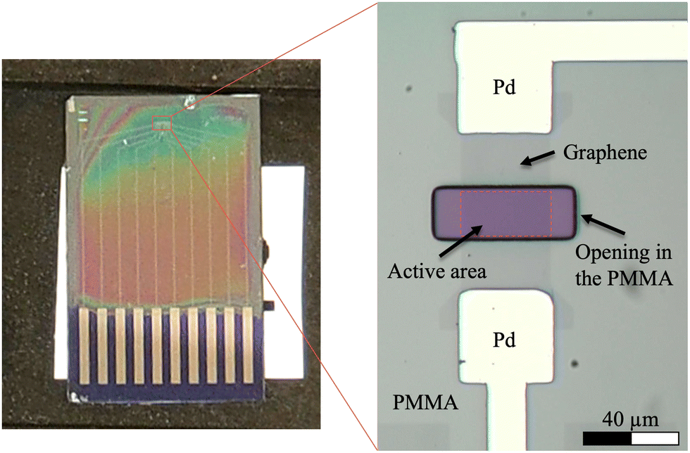 | ||
| Fig. 1 Optical images of the final device design. The whole chip (Left) and a close-up on one of the FETs at the very tip of the chip (Right). The active area dimensions are 40 × 20 μm2. Note that the borders of the opening have not been annotated. Instead, this is how the walls of the PMMA opening are perceived with an optical microscope. | ||
2.2 Two-photon oxidation and Raman characterization
2PO of graphene was carried out with a 515 nm femtosecond laser (Pharos-10, Light Conversion Ltd., 600 kHz repetition rate, 250 fs pulse duration) in ambient atmosphere at a relative humidity of 35%. We used a 4× objective with a spot diameter of 6.5 μm. The pulse energies ranged from 1 to 4 nJ and the irradiation time was 0.1 s spot−1.27 (= dosage range 0.1–1.6 nJ2s, see ESI† for details) As the achieved oxidation level with 2PO depends on many variables, not just the irradiation dose, Raman spectroscopy was used to determine the oxidation level. Raman spectra were measured using a DXR Raman Microscope (Thermo Scientific) with a 50x objective, laser excitation of 532 nm and power of 1 mW before and after oxidation to determine the level of oxidation achieved.2.3 pH solution preparations
For the pH measurements, self-prepared 28 mM BIS-TRIS propane HCl/KCl (BTPH) buffers were used. The different pH values were achieved by adding 2 M HCl to a 10 mM BIS-TRIS propane solution. To ensure that all the solutions were equally conductive, 2 M KCl was added until every solution had the same total concentration. The resulting final concentration was 28 mM ([BIS-TRIS] + [HCl] + [KCl]). The final solutions had concentration ratios of 1:5, 2:4, 3:3, 4:2 and 5:1 for HCl and KCl. After the solutions were prepared, their pH values were measured using Mettler Toledo FiveEasy pH meter with an InLab Micro Pro-ISM pH electrode.
2.4 pH measurements
The pH measurements were made with a measurement setup built from commercial devices. The devices used were a digital to analogue converter (DAC) (BNC-2090, National Instruments), digital multimeter (model 2000, Keithley), current amplifier (model 564, HMS Elektronik) and two preamplifiers (model 1201, DL Instruments). The connection to the sample was achieved by using a custom BNC to HDMI adapter and a standard HDMI cable. The HDMI cable was used as the connection to the sample, as it was an easy-to-use, commercial, and spring-loaded connection that proved to be very reliable. This was chosen over traditional wire bonding, as the latter was found to be tedious, unreliable, and added unnecessary fabrication steps. To our knowledge, this is the first reported use of this type of connector for GFET pH sensors. With the HDMI connection, it will be easy to realize practical applications of the sensor device.A self-written LabView program was used to control the measurement devices. During measurements, a bias voltage (UDS) of around 0.2 V was used in order to limit the current through the graphene to non-destructive levels. This was calculated using a series resistor and the actual sample as a potential divider. The gate electrode used was a commercial flexible Ag/AgCl dri-ref reference electrode FLEXREF (WPI) and the leakage current through it was monitored so that it was possible to subtract it from the measured drain-source current. Usually, the leakage current was in the range of nA. The gate electrode was held in place by the solution chamber so that the distance from the gate to the GFET was a constant, approximately 1.5 cm. A schematic and illustration of the SG-FET measurement geometry are presented in Fig. 2(a) and (b).
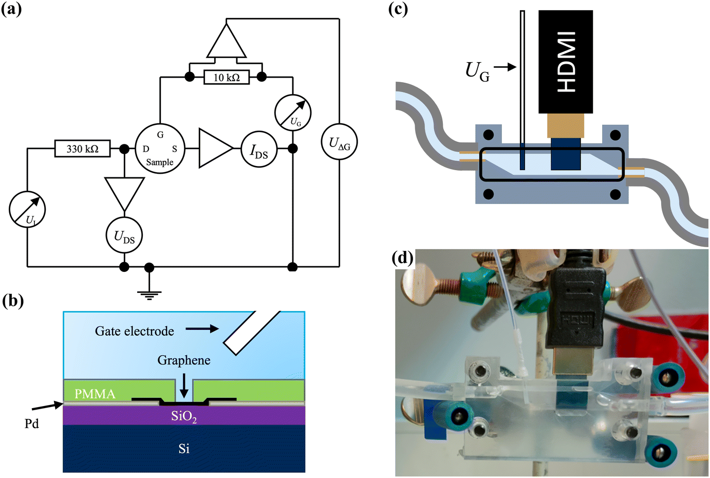 | ||
| Fig. 2 Illustrations of (a) the used measurement setup, (b) GFET measurement geometry (c) the in-house built solution chamber, and (d) an optical image of the said chamber. | ||
The pH dependency of the devices was determined by placing the sample (with 5 devices) into an in-house built solution chamber with a volume of roughly 2 ml (Fig. 2(c) and (d)). The sample was left to soak in a buffer solution for approximately 25 hours before starting the measurements, as it has been reported28 to reduce the amount of drift when there are PMMA residues present on the graphene by countering the doping caused by the residues. The solution was changed by pumping the buffer from a separate container. This way the sample was never dry during measurements, so the number of wet-dry cycles the sample experienced was reduced. This in turn reduced the risk of breaking the sample and prevented the deposition of salt on the graphene due to evaporation. The pump used was an in-house built peristaltic pump, connected to the chamber via standard silicone tubing. The measurements were always started from basic conditions (pH 9.50), going to neutral (pH 6.88) and then coming back to the basic conditions to see how stable the sample was and whether there was any drift or hysteresis present in the response.
The pH measurement data was processed automatically with a custom Python script. From the raw drain-source current (IDS) and potential (UDS) data, the resistance (RDS) was calculated. To automatically find the Dirac point location (UDirac), a Savitzky-Golay filter smoothening function was used. After the smoothening, the maximum resistance value location was used to determine the UDirac.
3 Results and discussion
All the GFET samples used were characterized with Raman spectroscopy. The data is presented in Fig. 3. As the oxidation level increased, the D band increased, the G band shifted, decreased, and became broader, the D′ appeared and increased, the 2D decreased and broadened, and the D + D′ behaved like a combination of D and D′ as it appeared and increased. From the Raman spectra, the ratio of intensities of the D and G peaks (I(D)/I(G)) was calculated by fitting the peaks with a Lorentzian function using Origin Pro. This ratio was used to determine the oxidation level of the devices.23,29 (See Fig S1 for the correlation between the laser irradiation dose and I(D)/I(G) ratio, ESI†) The higher oxidation level is seen as an increase in the ratio until it starts declining after graphene has become sufficiently disordered.29 An example of this behaviour was seen in a sample which reached highest I(D)/I(G) ratio of 3.58 at lower irradiation dose than the more irradiated sample showing a I(D)/I(G) ratio of 3.46. The higher oxidation level can also be seen from the full width at half maximum (FWHM) of the G and 2D bands as the peaks broaden with higher oxidation level.29 By comparing the I(D)/I(G) ratio and the spectra with the ref. 23, we estimate that the highest oxidation levels in this study correspond to overall oxidation levels from a few % to about 10%.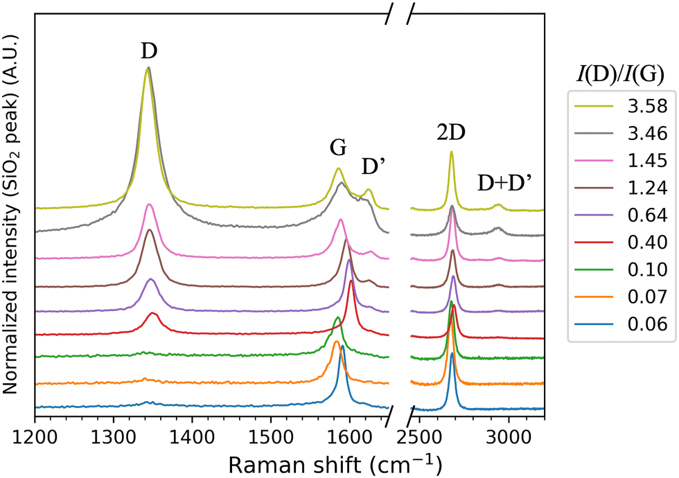 | ||
| Fig. 3 Raman spectra of the GFET devices used in the pH measurements sorted by their I(D)/I(G) ratio corresponding to different oxidation levels. Ratios 0.06–0.10 correspond to non-oxidized devices. Each spectrum is an average of 8–10 spectra and has been normalized by the maxima of the Si-peak (not shown), which has been set to 500 and then the spectra have been offset with the value 250. | ||
After Raman characterization, the devices had their pH response measured. Representative measurement data for a pristine and an oxidized GFET sample are presented in Fig. 4. See the ESI† for a summary of all of the measurement data used in this paper (Fig. S4, ESI†) and all the corresponding raw data (Table S3, ESI†). With the shown pristine graphene device, two random current spikes were detected, but they do not affect the analysis. They were most likely due to movement of wires in the measurement setup during the measurement. Also, the initial measurement in pH 9.50 has been left out of the data as it was clear that the device had not yet stabilized, and the single measurement point was an outlier. The data shown here is for the exact same device before and after laser-oxidation. Some of the samples were characterized in both pristine and oxidized state, and this sample history is shown in Table S2 (ESI†).
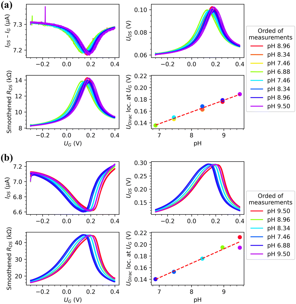 | ||
| Fig. 4 Representative measurement data for a single pH measurement for (a) pristine (I(D)/I(G) = 0.06) and (b) highly oxidized (I(D)/I(G) = 1.45) samples. Both include the measured drain-source current that has been normalized by removing the detected leakage current (IDS–IG, top left), measured drain-source potential (UDS, top right), smoothened drain-source resistance that is calculated from IDS and UDS (bottom left) and the found locations of Dirac points (UDirac loc. at UG) for each measurement in each pH measured (bottom right). The errors of the bottom right panels of both figures are of the magnitude of the size of the dots. See ESI† (Fig. S5) for more precise fitting data and directionality of the of the pH measurements. | ||
When looking at the location of the Dirac point for the pristine device, we can see that it was not around 0 V. This was most likely due to the final EBL step leaving residual PMMA onto the graphene and the SiO2 substrate. It has been reported28 that PMMA residues and SiO2 substrate cause p-type doping and therefore shift the Dirac point. Others have observed this to sometimes be a continuous, approximately 1 nm thick layer that had significant effect on the sensory function of graphene.30
It can be seen from Fig. 4 that the 2PO treatment does not always cause significant additional p-type doping compared to nominally pristine graphene, as the Dirac point is almost at the same location with both non-oxidized (I(D)/I(G) = 0.06) and oxidized (I(D)/I(G) = 1.45) devices when the solution is around pH 7. This lack of shifting could be due to the initial p-type doping being high because of the PMMA residues on the sample. However, with the sample of I(D)/I(G) ratio 0.10 2PO seems to increase amount of p-type doping on the sample. When it was oxidized to 3.46 I(D)/I(G) ratio, the Dirac point location shifts approximately 7–8 mV when in neutral pH. Therefore, the additional doping caused by 2PO seems to have been dependent on the initial doping level. In addition to the shift, some broadening of the transfer curve is visible, when the oxidation level increased. The transconductance of the GFETs increases with the oxidation level, but after an initial increase the charge carrier mobility decreases. (See ESI† for plots, Fig. S2) This would indicate that we are somehow removing impurities from the graphene with low levels of 2PO. Based on the I(D)/I(D′) ratio, introduction of sp3 groups caused the broadening when the oxidation level was low (see Fig. S3b, ESI†)).31–33 At high doses the broadening was caused by the formation of vacancies.31–33 We did not observe a significant degree of hysteresis when measuring the response to gate voltage sweeps at a single pH with pristine or oxidized devices.
The sensitivity dependence on the I(D)/I(G) ratio is shown in Fig. 5. The data shows that 2PO changes the pH sensitivity of GFET devices and, in particular, the sensitivity increases for higher oxidation levels. Alternate plots for correlating the sensitivity with other Raman parameters are shown in the ESI† (Fig. S3). The sensitivity increased as the oxidation level rose. However, the behaviour was not monotonic. Starting from the nominally pristine samples, the sensitivity first decreased. We believe that this was because the devices had some PMMA residues from the final EBL step, similarly to previous reports.30 The presence of PMMA had an effect similar to the laser-functionalization, making graphene more sensitive to pH. When the PMMA contaminated graphene was irradiated with the laser, it was possible that the polymer is broken and therefore the graphene was partially cleaned.34 The lowest sensitivity was reached at the irradiation level corresponding to the I(D)/I(G) of 0.64, after which the sensitivity started increasing with increasing irradiation dose. The sensitivity reached a plateau around I(D)/I(G) of 1.5 and did not change much after that. In this range, the sensitivity increased from ∼19 mV pH−1 to ∼25 mV pH−1, i.e., by about 32%. The fit presented in Fig. 5 is calculated starting from the sample with the lowest oxidation dose used to illustrate the trend of the effect that the oxidation has on the sensitivity. The functional form of the fit had no physical significance. When comparing these results to other published methods, it is important to note that it has been reported35 that the absolute value of the sensitivity achieved is dependent on the ionic species present in the solution. Additionally, it is known that comparing GFET pH sensitivities between publications is difficult.14,17,35
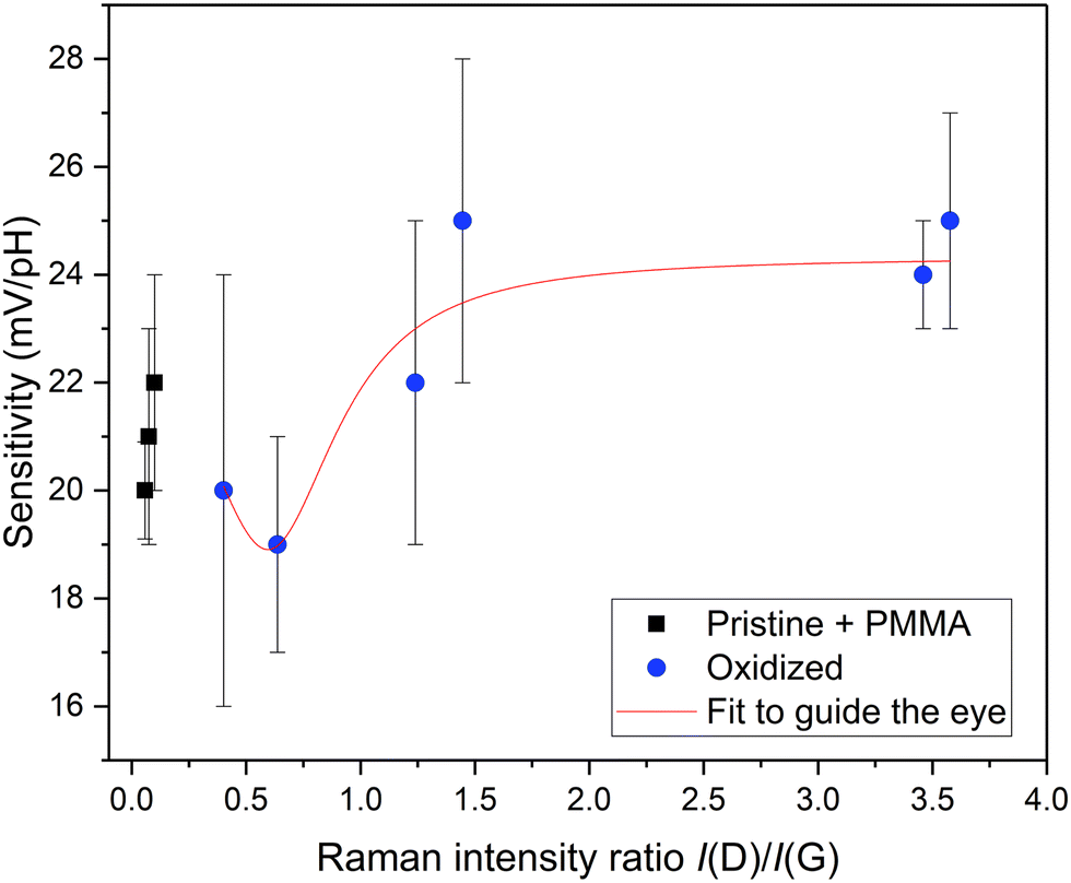 | ||
| Fig. 5 Effect of 2PO on the pH dependency of SG-GFETS. The error bars show the error of the fit. | ||
The main result of Fig. 5 is that 2PO could be used to tune and improve the sensitivity of GFETs. Although the improvement in the sensitivity compared to nominally pristine graphene was modest, about 14–25%, it would presumably be much larger for truly clean graphene, as shown by the 32% increase between mildly oxidized and strongly oxidized graphene. One of the advantages of the 2PO method for sensitivity tuning is that it enables optimization of the conditions for not only pH sensing but also simultaneously for other properties, such as functionalization of the GFET for immobilization of molecules on it. For example, 2PO has been shown to promote protein functionalization by non-covalent bonding with high local selectivity.36 Therefore, it should be possible to use 2PO to fabricate a biosensor with proteins binding to very specific areas. As 2PO offers very high control on where the oxidized patterns are, a reference device could be fabricated right next to the actual measurement device with only some μm of distance between them. Finally, a significant advantage of the 2PO method is that it is very simple, it works in ambient air, and it does not require any additional chemicals or tedious and expensive fabrication steps. Thus, it has high potential for becoming a manufacturing technology for applications, as the scale of the oxidation is essentially hampered only by the size of the moving stage used during oxidation.
Conclusions
Laser-induced two-photon oxidation of graphene was used for tuning and enhancing the sensitivity of a GFET pH sensor controllably. The highest achieved sensitivity was (25 ± 2) mV pH−1. The response of pristine graphene was affected by PMMA residues, and this should be taken into account during the device fabrication. It could be possible to avoid this problem by using a material as the passivation layer that can be annealed. (e.g., AlO2) The residues led to the absolute increase in sensitivity for 2PO GFETs to be quite small (14–25%). However, 2PO did initially seem to clean the graphene from PMMA residues at low irradiation levels, so that with a low oxidation level (I(D)/I(G) = 0.64) the lowest pH sensitivity was observed: (19 ± 2) mV pH−1. From this the increase in sensitivity reached with 2PO was approximately 32%.2PO provides a high level of control in both the oxidation level and the location of the oxidized patterns. It is an easy and fast oxidation method, and we believe it has a lot of potential to advance future sensor applications e.g., in the field of biosensors.
Author contributions
A. L. conducted the experiments, data analysis and analysis related programming. A. L. and E. S. designed the samples and wrote the first draft. A. L., E. S., and A. J. designed the experiments and experimental setup and built it. A. E. conducted the oxidation, majority of the Raman measurements and planned the Raman data analysis. A. E. and P. M. developed and built the oxidation setup. A. J. and M. P. supervised the research. A. L., E. S., A. E., A. J., and M. P. contributed to the discussion and manuscript editing.Conflicts of interest
There are no conflicts to declare.Acknowledgements
Authors would like to acknowledge the valuable technical work provided by Olli Rissanen and the practical help of Jyrki Manninen in building the measurement setup. Also, we thank for the research funding provided by Emil Aaltonen foundation and Jane and Aatos Erkko foundation.References
- P. Solís-Fernández, S. Okada, T. Sato, M. Tsuji and H. Ago, ACS Nano, 2016, 10, 2930–2939 CrossRef PubMed.
- C. I. L. Justino, A. R. Gomes, A. C. Freitas, A. C. Duarte and T. A. P. Rocha-Santos, TrAC, Trends Anal. Chem., 2017, 91, 53–66 CrossRef CAS.
- X. Tan, H. J. Chuang, M. W. Lin, Z. Zhou and M. M. C. Cheng, J. Phys. Chem. C, 2013, 117, 27155–27160 CrossRef CAS.
- S. S. Kwon, J. Yi, W. W. Lee, J. H. Shin, S. H. Kim, S. H. Cho, S. Nam and W. Il Park, ACS Appl. Mater. Interfaces, 2016, 8, 834–839 CrossRef CAS PubMed.
- J. Gao, Y. Wang, Y. Han, Y. Gao, C. Wang, L. Han and Y. Zhang, J. Mater. Sci.: Mater. Electron., 2020, 31, 15372–15380 CrossRef CAS.
- S. Falina, M. Syamsul, Y. Iyama, M. Hasegawa, Y. Koga and H. Kawarada, Diamond Relat. Mater., 2019, 91, 15–21 CrossRef CAS.
- B. Melai, P. Salvo, N. Calisi, L. Moni, A. Bonini, C. Paoletti, T. Lomonaco, V. Mollica, R. Fuoco and F. Di Francesco, 2016 38th Annual International Conference of the IEEE Engineering in Medicine and Biology Society (EMBC), IEEE, 2016, pp. 1898–1901.
- B. Mailly-Giacchetti, A. Hsu, H. Wang, V. Vinciguerra, F. Pappalardo, L. Occhipinti, E. Guidetti, S. Coffa, J. Kong and T. Palacios, J. Appl. Phys., 2013, 114, 084505 CrossRef.
- P. K. Ang, W. Chen, A. T. S. Wee and P. L. Kian, J. Am. Chem. Soc., 2008, 130, 14392–14393 CrossRef CAS PubMed.
- Y. Ohno, K. Maehashi, Y. Yamashiro and K. Matsumoto, Nano Lett., 2009, 9, 3318–3322 CrossRef CAS PubMed.
- I. Y. Sohn, D. J. Kim, J. H. Jung, O. J. Yoon, T. Nguyen Thanh, T. Tran Quang and N. E. Lee, Biosens. Bioelectron., 2013, 45, 70–76 CrossRef CAS PubMed.
- N. Lei, P. Li, W. Xue and J. Xu, Meas. Sci. Technol., 2011, 22, 107002 CrossRef.
- W. Fu, C. Nef, A. Tarasov, M. Wipf, R. Stoop, O. Knopfmacher, M. Weiss, M. Calame and C. Schönenberger, Nanoscale, 2013, 5, 12104–12110 RSC.
- P. Salvo, B. Melai, N. Calisi, C. Paoletti, F. Bellagambi, A. Kirchhain, M. G. Trivella, R. Fuoco and F. Di Francesco, Sens. Actuators, B, 2018, 256, 976–991 CrossRef CAS.
- P. K. Ang, W. Chen, A. T. S. Wee and P. L. Kian, J. Am. Chem. Soc., 2008, 130, 14392–14393 CrossRef CAS PubMed.
- J. Ristein, W. Zhang, F. Speck, M. Ostler, L. Ley and T. Seyller, J. Phys. D. Appl. Phys., 2010, 43, 345303 CrossRef.
- W. Fu, C. Nef, O. Knopfmacher, A. Tarasov, M. Weiss, M. Calame and C. Schönenberger, Nano Lett., 2011, 11, 3597–3600 CrossRef CAS PubMed.
- B. Mailly-Giacchetti, A. Hsu, H. Wang, V. Vinciguerra, F. Pappalardo, L. Occhipinti, E. Guidetti, S. Coffa, J. Kong and T. Palacios, J. Appl. Phys., 2013, 114, 084505 CrossRef.
- B. M. Giacchetti, A. Hsu, H. Wang, K. K. Kim, J. Kong and T. Palacios, MRS Proc., 2011, 1283, mrsf10-1283-b03-07 CrossRef.
- R. Sha, K. Komori and S. Badhulika, IEEE Sens. J., 2017, 17, 5038–5043 CAS.
- G. Williams, B. Seger and P. V. Kamt, ACS Nano, 2008, 2, 1487–1491 CrossRef CAS PubMed.
- L. Liu, D. Xie, M. Wu, X. Yang, Z. Xu, W. Wang, X. Bai and E. Wang, Carbon, 2012, 50, 3039–3044 CrossRef CAS.
- A. Johansson, H. C. Tsai, J. Aumanen, J. Koivistoinen, P. Myllyperkiö, Y. Z. Hung, M. C. Chuang, C. H. Chen, W. Y. Woon and M. Pettersson, Carbon, 2017, 115, 77–82 CrossRef CAS.
- J. Aumanen, A. Johansson, J. Koivistoinen, P. Myllyperkiö and M. Pettersson, Nanoscale, 2015, 7, 2851–2855 RSC.
- E. S. Orth, J. G. L. Ferreira, J. E. S. Fonsaca, S. F. Blaskievicz, S. H. Domingues, A. Dasgupta, M. Terrones and A. J. G. Zarbin, J. Colloid Interface Sci., 2016, 467, 239–244 CrossRef CAS PubMed.
- T. Taniguchi, S. Kurihara, H. Tateishi, K. Hatakeyama, M. Koinuma, H. Yokoi, M. Hara, H. Ishikawa and Y. Matsumoto, Carbon, 2015, 84, 560–566 CrossRef CAS.
- K. K. Mentel, A. V. Emelianov, A. Philip, A. Johansson, M. Karppinen and M. Pettersson, Adv. Mater. Interfaces, 2022, 9, 2201110 CrossRef CAS.
- N. Miyakawa, A. Shinagawa, Y. Kajiwara, S. Ushiba, T. Ono, Y. Kanai, S. Tani, M. Kimura and K. Matsumoto, Sensors, 2021, 21, 7455 CrossRef CAS PubMed.
- X. Díez-Betriu, S. Álvarez-García, C. Botas, P. Álvarez, J. Sánchez-Marcos, C. Prieto, R. Menéndez and A. De Andrés, J. Mater. Chem. C, 2013, 1, 6905–6912 RSC.
- Y. Dan, Y. Lu, N. J. Kybert, Z. Luo and A. T. C. Johnson, Nano Lett., 2009, 9, 1472–1475 CrossRef CAS PubMed.
- A. Eckmann, A. Felten, A. Mishchenko, L. Britnell, R. Krupke, K. S. Novoselov and C. Casiraghi, Nano Lett., 2012, 12, 3925–3930 CrossRef CAS PubMed.
- A. V. Emelianov, D. Kireev, D. D. Levin and I. I. Bobrinetskiy, Appl. Phys. Lett., 2016, 109, 173101 CrossRef.
- H. S. Song, S. L. Li, H. Miyazaki, S. Sato, K. Hayashi, A. Yamada, N. Yokoyama and K. Tsukagoshi, Sci. Rep., 2012, 2, 1–6 Search PubMed.
- Y. Jia, X. Gong, P. Peng, Z. Wang, Z. Tian, L. Ren, Y. Fu and H. Zhang, Nano-Micro Lett., 2016, 8, 336–346 CrossRef PubMed.
- M. H. Lee, B. J. Kim, K. H. Lee, I. S. Shin, W. Huh, J. H. Cho and M. S. Kang, Nanoscale, 2015, 7, 7540–7544 RSC.
- E. D. Sitsanidis, J. Schirmer, A. Lampinen, K. K. Mentel, V. M. Hiltunen, V. Ruokolainen, A. Johansson, P. Myllyperkiö, M. Nissinen and M. Pettersson, Nanoscale Adv., 2021, 3, 2065–2074 RSC.
Footnote |
| † Electronic supplementary information (ESI) available: Full Raman data fitting parameters, alternative sensitivity correlation plots, sample history, and full sensitivity fitting data. See DOI: https://doi.org/10.1039/d3cp00359k |
| This journal is © the Owner Societies 2023 |