
Piezoelectric ferromagnetism in Janus monolayer YBrI: a first-principles prediction†
San-Dong
Guo
 *a,
Meng-Xia
Wang
a,
Yu-Ling
Tao
a and
Bang-Gui
Liu
bc
*a,
Meng-Xia
Wang
a,
Yu-Ling
Tao
a and
Bang-Gui
Liu
bc
aSchool of Electronic Engineering, Xi'an University of Posts and Telecommunications, Xi'an, 710121, China. E-mail: sandongyuwang@163.com
bBeijing National Laboratory for Condensed Matter Physics, Institute of Physics, Chinese Academy of Sciences, Beijing, 100190, People's Republic of China
cSchool of Physical Sciences, University of Chinese Academy of Sciences, Beijing, 100190, People's Republic of China
First published on 29th November 2022
Abstract
Coexistence of intrinsic ferromagnetism and piezoelectricity, namely piezoelectric ferromagnetism (PFM), is crucial to advance multifunctional spintronic technologies. In this work, we demonstrate that Janus monolayer YBrI is a PFM, which is dynamically, mechanically and thermally stable. The electronic correlation effects on the physical properties of YBrI are investigated by using generalized gradient approximation plus U (GGA+U) approach. For out-of-plane magnetic anisotropy, YBrI is a ferrovalley (FV) material, and its valley splitting is larger than 82 meV within the considered U range. The anomalous valley Hall effect (AVHE) can be achieved under an in-plane electric field. However, for in-plane magnetic anisotropy, YBrI is a common ferromagnetic (FM) semiconductor. When considering intrinsic magnetic anisotropy, the easy axis of YBrI is always in-plane, and its magnetic anisotropy energy (MAE) varies from 0.309 meV to 0.237 meV (U = 0.0 eV to 3.0 eV). However, the magnetization can be adjusted from the in-plane to out-of-plane direction by an external magnetic field, and then lead to the occurrence of valley polarization. Moreover, the missing centrosymmetry along with broken mirror symmetry results in both in-plane and out-of-plane piezoelectricity in the YBrI monolayer. At a typical U = 2.0 eV, the piezoelectric strain coefficient d11 is predicted to be −5.61 pm V−1, which is higher than or comparable with the ones of other known two-dimensional (2D) materials. The electronic and piezoelectric properties of YBrI can be effectively tuned by applying biaxial strain. For example, tensile strain can enhance valley splitting and d11 (absolute value). The predicted magnetic transition temperature of YBrI is higher than those of experimentally synthesized 2D FM materials CrI3 and Cr2Ge2Te6. Our findings of these distinctive properties could pave the way for designing multifunctional spintronic devices, and bring forward a new perspective for constructing 2D materials.
1 Introduction
2D materials have attracted much attention due to their unique properties and potential applications in future nanodevices.1 The reduction in dimensionality of 2D materials results in inversion symmetry often being eliminated, which allows these materials to become piezoelectric.2 The MoS2 monolayer is a classic 2D piezoelectric material, which is first predicted theoretically,3 and then confirmed experimentally.4 In addition to piezoelectric properties, magnetism in 2D systems is also one of the most fascinating properties of materials, and long-range magnetic order should be prohibited according to the Mermin–Wagner theorem.5 However, the intrinsic long-range FM order in 2D semiconductors such as Cr2Ge2Te6 and CrI36,7 has been achieved experimentally, which is due to spin–orbital coupling (SOC)-induced magnetic anisotropy. 2D magnetic materials provide a new platform for valleytronics. Valley is emerging as a new degree of freedom, which can be used to manipulate information.8,9 To achieve valley application, valley polarization should be induced. A 2D magnetic material with a special crystal structure provides an opportunity to realize spontaneous valley polarization, which is known as an FV material.10Compared with 2D materials with individual piezoelectric or magnetic or valley properties, 2D multifunctional materials may give rise to unprecedented opportunities for intriguing physics, and produce novel device applications.11 Coexistence of intrinsic ferromagnetism and piezoelectricity has been reported in some 2D systems.12–15 The strong out-of-plane piezoelectricity is predicted in the CrBr1.5I1.5 monolayer as a PFM, and the d31 is larger than 1.0 pm V−1.14 The FV materials possess magnetism and lack spatial inversion-symmetry,10 which make these materials PFMs. To realize AVHE, a possible way is proposed in FV monolayer GdCl2 by the piezoelectric effect, not an external electric field, namely the piezoelectric anomalous valley Hall effect (PAVHE).16 The piezoelectricity and FV properties in Janus monolayer VClBr are investigated, and a giant in-plane piezoelectricity is predicted.17
Recently, YX2 (X = I, Br and Cl) monolayers are predicted to be dynamically and thermally stable 2D FM semiconductors.18 Large spontaneous valley polarizations are also reported,18 but their magnetic anisotropy is not considered. Out-of-plane magnetic anisotropy is key to producing spontaneous valley polarization in a 2D hexagonal lattice or for technological applications in a ferromagnetism-related heterostructure.19–24 For example, for monolayer FeClF, increasing electron correlation effects can induce the coexistence of FV and a quantum anomalous Hall (QAH) state with fixed out-of-plane magnetic anisotropy, but the spontaneous valley polarization will disappear for the in-plane case.20
In this work, taking Janus monolayer YBrI as a derivative of YX2 (X = I, Br and Cl) as an example, we investigate its magnetic, electronic and piezoelectric properties. Our results show that monolayer YBrI is dynamically, mechanically and thermally stable, and is intrinsically a common FM semiconductor due to inherent in-plane magnetic anisotropy. To achieve FV properties, an external magnetic field is needed to adjust the magnetization from an in-plane to out-of-plane direction. With breaking horizontal mirror symmetry, both in-plane and out-of-plane piezoelectricity can be induced in the YBrI monolayer with an imposed uniaxial in-plane strain. At a typical U = 2.0 eV, the predicted d11 (−5.61 pm V−1) is higher than or comparable with ones of other 2D known materials.2,3 The calculated results show that the strain can effectively tune the electronic and piezoelectric properties of YBrI. The predicted magnetic transition temperature of YBrI is higher than those of experimentally synthesized CrI3 and Cr2Ge2Te6 ferromagnets.6,7 Our work implies that the Janus monolayer YBrI is a potential multifunctional material with possible applications in spintronics and piezoelectronics.
2 Computational details
Our spin-polarized first-principles calculations are performed by means of density functional theory (DFT)25,26 with projector-augmented-wave (PAW) potential and plane-wave basis, as implemented in the VASP code.27–29 The exchange-correlation functional is tackled by generalized gradient approximation of Perdew, Burke and Ernzerhof (PBE-GGA).30 A kinetic energy cutoff of 500 eV, a force convergence criterion of less than 0.0001 eV Å−1, and a total energy convergence criterion of 10−8 eV are adopted to attain reliable results. The GGA+U scheme by the rotationally invariant approach proposed by Dudarev et al.31 is adopted to account for the strong correction effect for the localized Y-4 d electrons. A vacuum region of 20.76 Å along the z direction is used to eliminate the image interaction between adjacent layers. The SOC effect is fully considered in the calculations of both the band structure and MAE. The MAE calculation includes two steps: (i) a collinear self-consistent field calculation is performed without SOC to obtain the convergent charge density; (ii) a noncollinear non-self-consistent calculation of two different magnetization directions (in-plane and out-of-plane directions) is carried out within SOC.The phonon dispersions with the FM ground state are calculated through the finite-displacement supercell method with the 5 × 5 × 1 supercell, as implemented in the Phonopy code.32Ab initio molecular dynamics (AIMD) simulation over a 4 × 4 × 1 supercell is performed in the canonical ensemble for 8 ps with a time step of 1.0 fs, where the temperature is controlled at 300 K. The Berry curvatures of the YBrI monolayer are calculated directly from the calculated wave functions, based on Fukui's method,33 as implemented in the VASPBERRY code.34,35 The elastic stiffness tensor Cij and piezoelectric stress tensor eij are carried out by using the strain–stress relationship and density functional perturbation theory (DFPT) method.36 The 2D C2Dij/e2Dij have been renormalized by C2Dij = LzC3Dij/e2Dij = Lze3Dij, in which Lz is the length of the unit cell along the z direction. The Brillouin zone (BZ) integration is sampled by using 21 × 21 × 1 Monkhorst-Pack grids for self-consistent calculations and Cij, and 12 × 21 × 1 k-points for FM/antiferromagnetic (AFM) energy and eij.
3 Structure and stability
In analogy to monolayer MoSSe,37,38 YBrI consists of a Br–Y–I sandwich layer. Each Y atom is surrounded by three Br and three I atoms, which forms a triangular prism. The top and side views of the crystal structure of YBrI are shown in Fig. 1, which can be constructed by replacing one of two Br/I layers with I/Br atoms in YBr2/YI2. As a result, the inequivalent bond lengths between Y–Br and Y–I reduce the symmetry from P![[6 with combining macron]](https://www.rsc.org/images/entities/char_0036_0304.gif) m2 to P3m1 and break the horizontal mirror symmetry, compared with monolayer YBr2/YI2. For the YBrI monolayer, the broken mirror symmetry leads to both in-plane and vertical piezoelectric polarizations, while only in-plane piezoelectric polarization exists in Ybr2/YI2. The optimized lattice constants are a = 3.99 Å with GGA (U = 0 eV). The energies of AFM (EAFM) and FM (EFM) configurations are calculated to determine the ground state of YBrI. Their energy difference (ΔE = EAFM − EFM) is 33.03 meV. ΔE > 0 indicates FM ordering, while ΔE < 0 means AFM ordering. Thus, YBrI is in the FM ground state.
m2 to P3m1 and break the horizontal mirror symmetry, compared with monolayer YBr2/YI2. For the YBrI monolayer, the broken mirror symmetry leads to both in-plane and vertical piezoelectric polarizations, while only in-plane piezoelectric polarization exists in Ybr2/YI2. The optimized lattice constants are a = 3.99 Å with GGA (U = 0 eV). The energies of AFM (EAFM) and FM (EFM) configurations are calculated to determine the ground state of YBrI. Their energy difference (ΔE = EAFM − EFM) is 33.03 meV. ΔE > 0 indicates FM ordering, while ΔE < 0 means AFM ordering. Thus, YBrI is in the FM ground state.
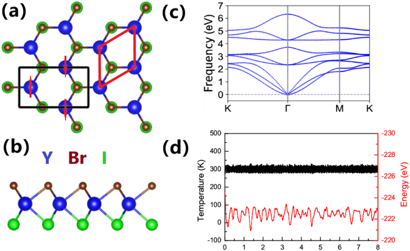 | ||
| Fig. 1 For a YBrI monolayer, (a) top view and (b) side view of the crystal structure. The primitive (rectangle supercell) cell is marked by red (black) lines, and the AFM configuration is shown with arrows in (a). (c) The phonon dispersion curves. (d) The temperature and total energy fluctuations as a function of simulation time (Unit: ps) at 300 K. | ||
Firstly, the cohesive energy (Ecoh) can be used to examine the feasibility of the experimental synthesis of YBrI. The formation energy can be calculated with respect to the convex hull and elemental states.39,40 For simplicity, the cohesive energy (Ecoh) is defined as Ecoh = EYBrI − EY − EBr − EI with respect to the elemental states, where EYBrI is the energy of the YBrI, and EY, EBr and EI are the energies of isolated atoms of Y, Br and I, respectively. The resultant cohesive energy is −2.35 eV for YBrI, which implies that YBrI is energetically stable.
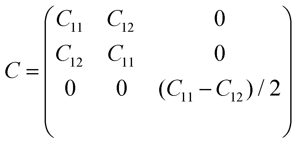
To evaluate the stability of YBrI, the phonon dispersion, molecular dynamics and elastic constant calculations were carried out by using the GGA exchange-correlation functional. The phonon spectrum is calculated to confirm the dynamic stability of YBrI (see Fig. 1). Because the primitive cell contains three atoms, the phonon dispersion possesses nine branches, including three acoustic and six optical modes. No imaginary frequencies can be observed in the YBrI monolayer, indicating its dynamic stability. To corroborate the thermal stability, the evolution of temperature and total energy vs time are calculated using AIMD at room temperature, which is plotted in Fig. 1. During the simulation period, with increasing time, the frameworks of YBrI are well preserved with little fluctuations of temperature and total energy, which confirms its thermal stability. Due to the P3m1 space group, using Voigt notation, the elastic tensor of YBrI can be reduced into:2
 | (1) |
The independent C11 and C12 of YBrI are 41.30 Nm−1 and 12.23 Nm−1. It can be seen that the YBrI monolayer satisfies the Born-Huang criteria of a 2D hexagonal plane41 (C11 > 0 and C11 − C12 > 0), which confirms its mechanical stability.
It has been reported that the electronic properties of monolayer FeClF, which has the same crystal structure as YBrI, are sensitive to electronic correlation effects.20 To study the electronic correlation effect of YBrI, the lattice constant a is optimized at different U (0–3 eV), as shown in Fig. 1 of the ESI.† It is found that a almost linearly increases with increasing U, and the change is only 0.054 Å. The energy difference of AFM and FM configurations as a function of U is calculated to determine the ground state of YBrI, which is plotted in Fig. 2. Within the considered U range, YBrI is always a FM ground state, and increasing U can strengthen the FM interaction.
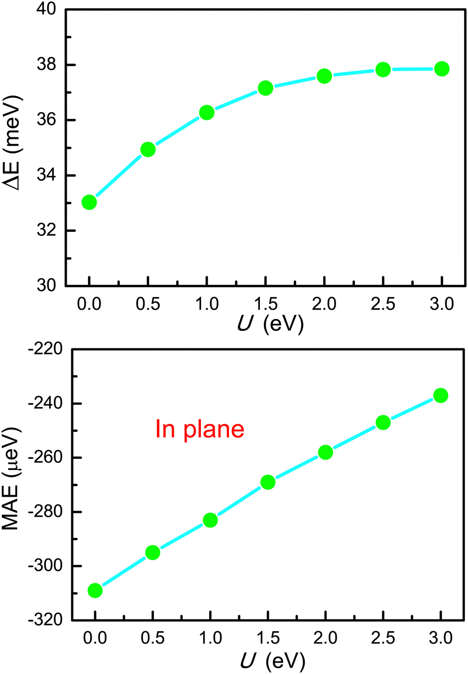 | ||
| Fig. 2 The energy differences ΔE between AFM and FM ordering and MAE as a function of U. | ||
4 Correlation effects
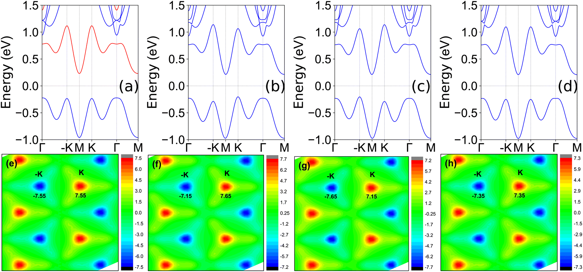
Electronic correlation and magnetic anisotropy have important effects on the electronic states of some 2D materials.19,20 For the FeClF monolayer, with fixed out-of-plane magnetic anisotropy, the increasing electron correlation effects can induce the FV to half-valley-metal (HVM) to QAH to HVM to FV transitions.20 However, for in-plane magnetic anisotropy, these novel electronic states will disappear. The YBrI has the same crystal structure with FeClF,20 and they have a sandwich structure with P3m1 symmetry. So, it is very necessary when using electronic state calculations of YBrI to consider electronic correlation and magnetic anisotropy. The energy band structure of YBrI without SOC and U = 0 eV is plotted in Fig. 1 of the ESI,† which can give better clarity on how the energy bands evolve upon the inclusion of different effects. It is an indirect gap semiconductor with a gap value of 0.254 eV, and the valence band maximum (VBM)/conduction band bottom (CBM) is located at the Γ/M point.Firstly, the out-of-plane magnetic anisotropy is assumed with varied U. The out-of-plane FM ordering maintains the horizontal mirror symmetry (for YBrI, the horizontal mirror symmetry has been removed by the special Janus structure), and breaks all possible vertical mirrors, which allows a spontaneous valley splitting. The evolutions of electronic band structures as a function of U are studied by GGA + SOC, and the energy band structures at representative U values are plotted in Fig. 3. It is clearly seen that they are all indirect gap semiconductors with VBM/CBM at the K/M point in the considered U range, and spontaneous valley splitting can be observed. This means that YBrI is a FV material. The valley splitting is defined as the energy difference between −K and K valleys (absolute value). The valley splitting and gap as a function of U are plotted in Fig. 4. For the FeClF monolayer, the gap closes, reopens, and then closes.20 However, the gap increases monotonically with increasing U for the YBrI monolayer, which means that no topological phase transition is produced. Although FeClF and YBrI monolayers have the same crystal structure, the outer electronic configurations of Y and Fe elements are different, which leads to a difference in the behavior of band evolution with U. For the top valence band, the general tendency of valley splitting (absolute value) increases with increasing U, while the reduced tendency is observed for that of the bottom conduction band. It should be highlighted that only valley polarization of the top valence band can be applied in practice, and the valley splitting (absolute value) is larger than 82 meV in the considered U range. This value is larger than those of many predicted FV materials such as VSe2, LaBr2 and VSi2N4 (33–78.2 meV).10,42–44
 | ||
| Fig. 3 The energy band structures of the YBrI monolayer with out-of-plane (top) or in-plane (bottom) magnetic anisotropy by using GGA + SOC at some representative U values. | ||
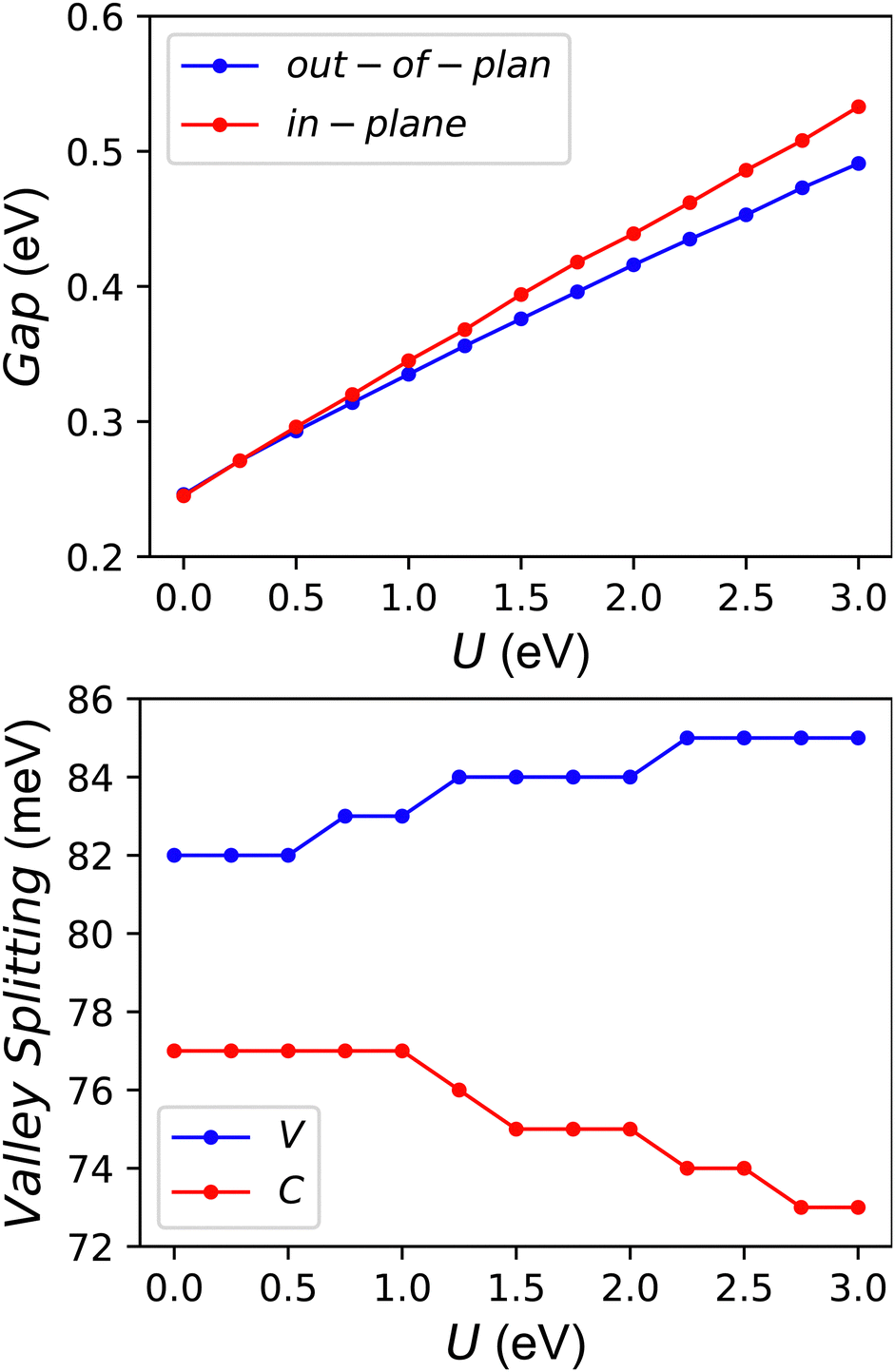 | ||
| Fig. 4 The gap (including out-of-plane and in-plane magnetic anisotropy) and valley splitting (including bottom conduction (C) and top valence (V) bands) as a function of U. | ||
With fixed in-plane magnetic anisotropy, the energy band structures at representative U values are also shown in Fig. 3, and the gaps vs. U are plotted in Fig. 4. It is clearly seen that YBrI is still an indirect gap semiconductor in the considered U range. The CBM is always at the M point, while the VBM changes from the Γ point to one point slightly deviated from the Γ to K point with increasing U. The gap of YBrI increases monotonically, when U increases. However, the −K and K valleys keep degenerating, which means that no spontaneous valley splitting can be observed. Similar results can be found in some 2D materials.19,20 For example, for FeClF,20 varied U produces no special QAH states and prominent valley polarization, which is very different from those with fixed out-of-plane magnetic anisotropy.
In view of the above discussion, it is very important to confirm intrinsic magnetic anisotropy of monolayer YBrI, which can be described by MAE. The MAE can be calculated by the energy difference of the magnetization orientation along the (100) and (001) cases. The positive values mean out-of-plane magnetic anisotropy, while negative values indicate an in-plane one. The MAE as a function of U is plotted in Fig. 2. It is clearly seen that the MAE of YBrI is always negative, indicating its in-plane magnetic anisotropy. The MAE changes from −0.309 meV to −0.237 meV, which means that increasing U can reduce MAE. So, YBrI intrinsically is not a FV material. However, the FV states can be achieved by an external magnetic field, which can change the in-plane magnetic anisotropy to an out-of-plane one.
Finally, taking a typical U = 2.0 eV, the electronic states of YBrI are investigated in detail. The spin-polarized band structures of monolayer YBrI by using both GGA and GGA + SOC are plotted in Fig. 5. According to Fig. 5(a), distinct spin splitting can be observed due to the exchange interaction, and YBrI is an indirect band gap semiconductor (gap of 0.463 eV) with VBM/CBM provided by the spin-up/spin-down. For both conduction and valence bands, the energies of valleys of −K and K are degenerate. Based on the projected band structure in Fig. 6, it is clearly seen that the only one electron occupies the top dz2-dominated valence band in the spin-up direction, while the other bottom dz2-dominated conduction band in the spin-dn direction is empty. This special electron configuration will lead to the magnetic moment of each Y atom being expected to be 1 μB. Fig. 5(b) shows that the valley polarization can be induced by SOC. The valley splitting of the top valence band is 84 meV, which is between those of YBr2 (58 meV) and YI2 (109 meV).18 The energy of the K valley is higher than that of the −K valley, and the valley polarization can be switched by reversing the magnetization direction (see Fig. 5(c)). Fig. 5(b and c) show that YBrI is an indirect band gap semiconductor with a gap value of 0.416 eV. When the magnetization direction of YBrI is in-plane along the x direction (see Fig. 5(d)), no valley polarization can be observed, and it is still an indirect band gap semiconductor with a gap value of 0.439 eV.
 | ||
| Fig. 5 The band structures (a–d) and Berry curvature distributions (e–h) of monolayer YBrI without SOC (a and e); with SOC (b, f), (c, g) and (d, h) for the magnetic moment of Y along the positive z, negative z, and positive x direction, respectively. In (a), the blue (red) lines represent the band structure in the spin-up (spin-down) direction. For all cases, U = 2 eV is adopted. | ||
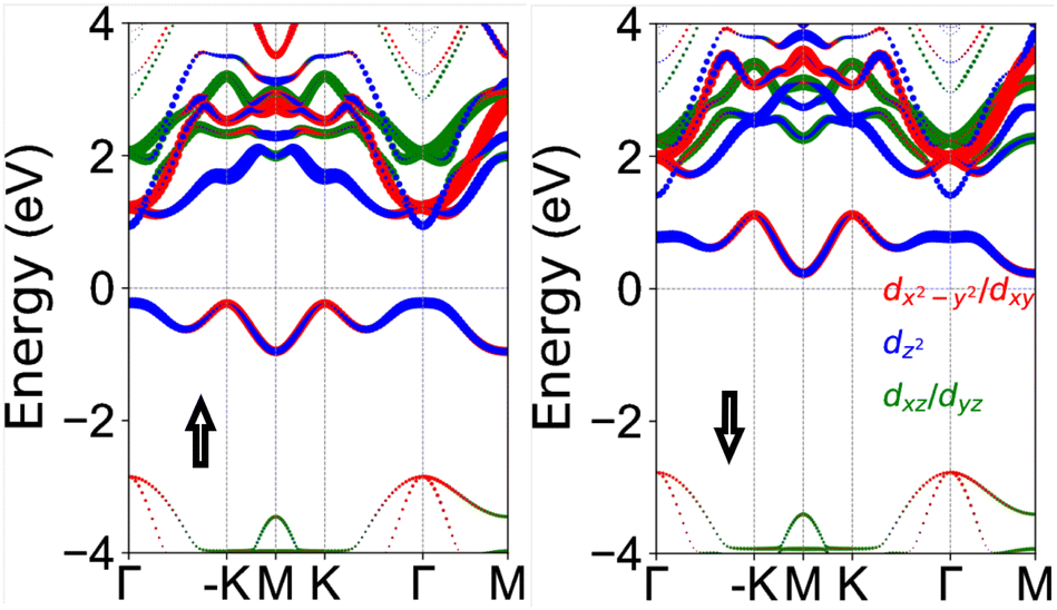 | ||
| Fig. 6 The Y-d-orbital characters of energy bands by using GGA+U (U = 2.0 eV), including spin-up and spin-down directions. | ||
According to Fig. 6, it is found that dx2−y2/dxy orbitals dominate −K and K valleys, which is very key to producing valley polarization. The valley polarization induced by SOC is mainly due to the intra-atomic interaction Ĥ0SOC (the interaction between the same spin states). For out-of-plane magnetization, Ĥ0SOC can be expressed as:10,45,46
Ĥ0SOC = α![[L with combining circumflex]](https://www.rsc.org/images/entities/i_char_004c_0302.gif) z z | (2) |
z is the orbital angular moment along the z direction, and α is the coupling strength. The resulting energy at K and −K valleys can be expressed as:| Eτ = 〈ϕτ|Ĥ0SOC|ϕτ〉 | (3) |
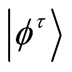 means the orbital basis for −K and K valleys, and the subscript τ represents the valley index (τ = ±1). If the −K and K valleys are mainly from dx2−y2/dxy orbitals, the valley splitting |ΔEV| at −K and K points can be written as:
| |ΔEV| = EK − E−K = 4α | (4) |
If the −K and K valleys are dominated by dz2 orbitals, the valley splitting |ΔE| is expressed as:
| |ΔEV| =EK − E−K = 0 | (5) |
For the dx2−y2/dxy-dominated −K/K valley, when the magnetization orientation is the general case, ΔEV = 4α![[thin space (1/6-em)]](https://www.rsc.org/images/entities/char_2009.gif) cosθ46 (θ = 0/90° means out-of-plane/in-plane direction). When the magnetocrystalline direction is along the in-plane one, the valley splitting of YBrI will be zero.
cosθ46 (θ = 0/90° means out-of-plane/in-plane direction). When the magnetocrystalline direction is along the in-plane one, the valley splitting of YBrI will be zero.
Fig. 5 also presents the calculated Berry curvature of YBrI as a contour map in 2D BZ with and without SOC. For all four situations, the opposite signs around −K and K valleys can be observed. For these situations without valley polarization, Berry curvatures show equal magnitudes at −K and K valleys. However, unequal magnitudes of Berry curvatures at −K and K valleys can be observed for those with valley polarization. When reversing the magnetization from the z to −z direction, the magnitudes of Berry curvature at −K and K valleys exchange to each other but their signs remain unchanged.
Under an in-plane longitudinal electric field E, the anomalous velocity υ of Bloch electrons is associated with Berry curvature Ω(k):υ ∼ E × Ω(k).47 Appropriate hole doping can move the Fermi level to fall between the −K and K valleys. This leads to only one valley having doped holes. When an in-plane electric field is applied, the Berry curvature forces the hole carriers to accumulate on one side of the sample, giving rise to an AVHE in monolayer YBrI. As illustrated in Fig. 7, when the K valley is doped with holes, the positive Berry curvature drives the spin-up holes to accumulate on the right side of the sample in the presence of an in-plane electric field. When the magnetization is reversed, the −K valley is doped with holes, and then the spin-down holes move to the left side of the sample due to the negative Berry curvature of the −K valley.
 | ||
| Fig. 7 Schematic AVHE for the hole-doped YBrI monolayer at the K (a) and −K (b) valleys under an in-plane electric field E. The arrows stand for the spin-up or spin-down states. | ||
5 Piezoelectric properties
The YBrI monolayer lacks inversion symmetry, and then it is piezoelectric. Moreover, both in-plane and vertical piezoelectric polarizations can be achieved due to the special Janus structure, which is the same with the Janus MoSSe monolayer.48 Based on the energy band structures above, Janus YBrI is a FM semiconductor, and its semiconductor properties are compatible with a practical piezoelectric material to prohibit current leakage. As such, piezoelectricity and magnetism can coexist in YBrI.Being analogous to the MoSSe monolayer,48 by performing symmetry analysis and only considering the in-plane strain and stress, the piezoelectric stress and strain tensors of YBrI with Voigt notation can be reduced into:2
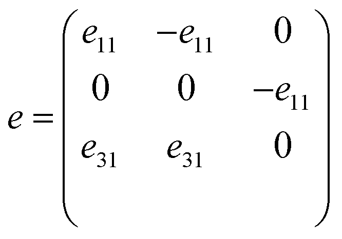 | (6) |
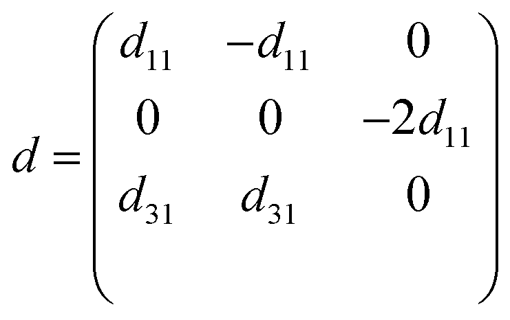 | (7) |
When a uniaxial in-plane strain is imposed, both in-plane and out-of-plane piezoelectric polarization can be induced (e11/d11 ≠ 0 and e31/d31 ≠ 0). However, with an applied biaxial in-plane strain, the in-plane piezoelectric response will disappear (e11/d11 = 0), but the out-of-plane piezoelectric polarization still maintains (e31/d31 ≠ 0). Here, the two independent d11 and d31 can be derived by eik = dijCjk
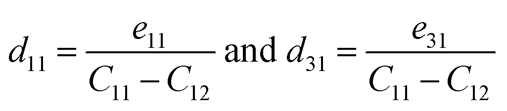 | (8) |
We use an orthorhombic supercell (see Fig. 1) as the computational unit cell to calculate the e11/e31 of YBrI. The elastic constants (C11, C12, C11 − C12 and C11 + C12) and piezoelectric stress coefficients (e11 and e31) along the ionic and electronic contributions as a function of U are shown in Fig. 2 and 3 of the ESI.†d11/d31vs. U are plotted in Fig. 8. It is found that C11, C12, C11 − C12, C11 + C12, e31 and d31 have weak dependence on U, and increasing U improves d11 (absolute value from 2.85 pm V−1 to 7.12 pm V−1) due to enhanced e11 (absolute value). It is found that the d31 is very small (−0.125 pm V−1 to −0.087 pm V−1 with increasing U). At a typical U = 2.0 eV,18 the calculated d11 is −5.61 pm V−1. The predicted absolute value of d11 (2.85–7.12 pm V−1 within the considered U range) is higher than or comparable with the ones of other 2D known materials.2,3 Thus, the YBrI monolayer is a PFM.
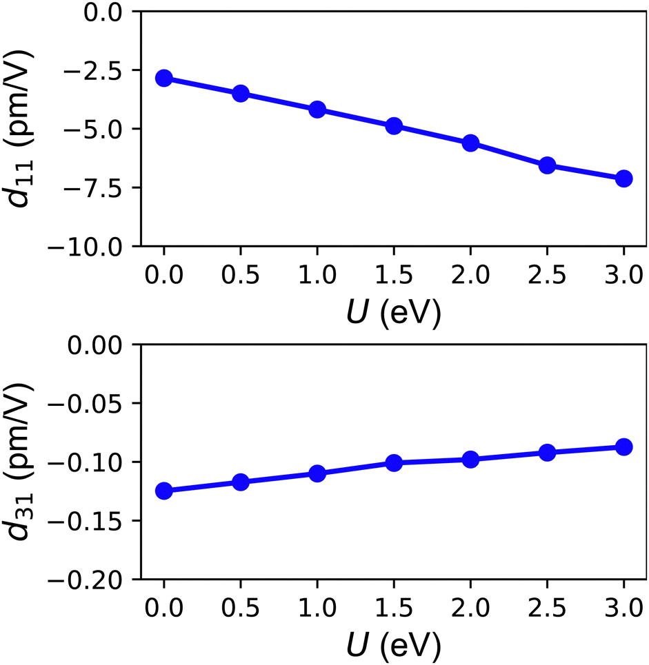 | ||
| Fig. 8 The piezoelectric strain coefficient d11 and d31 as a function of U. | ||
6 Strain effects
The electronic, piezoelectric, valley and topological properties of 2D materials can be easily tuned by strain engineering.49–52 We use a/a0 (0.94–1.06) to simulate biaxial strain, in which a/a0 denotes the strained/unstrained lattice constant. a/a0 < 1 indicates compressive strain, while a/a0 > 1 means tensile strain. Taking a typical U = 2.0 eV, the strain effects on the physical properties of YBrI are investigated.Fig. 9 shows the energy difference between AFM and FM ordering as a function of a/a0, and all strained YBrI are in the FM ground state in the considered strain range. It is found that compressive strain can enhance FM interactions, which is in favour of high Curie temperature. Within SOC, the strained energy band structures with both out-of-plane and in-plane magnetic anisotropy are plotted in Fig. 4 of the ESI,† and the corresponding gaps and valley splitting are shown in Fig. 10. With a/a0 from 0.94 to 1.06, YBrI is always a FM semiconductor for both out-of-plane and in-plane magnetic anisotropy. With increasing strain, the gap of YBrI firstly increases, and then decreases. For the out-of-plane case, the tensile strain can enhance valley splitting. According to Fig. 9, the inherent easy magnetization axis of YBrI is always in-plane in the considered strain range, which means that strained YBrI is a common FM semiconductor, not a FV material. So, the magnetic and electronic properties of YBrI monolayer are robust against strain.
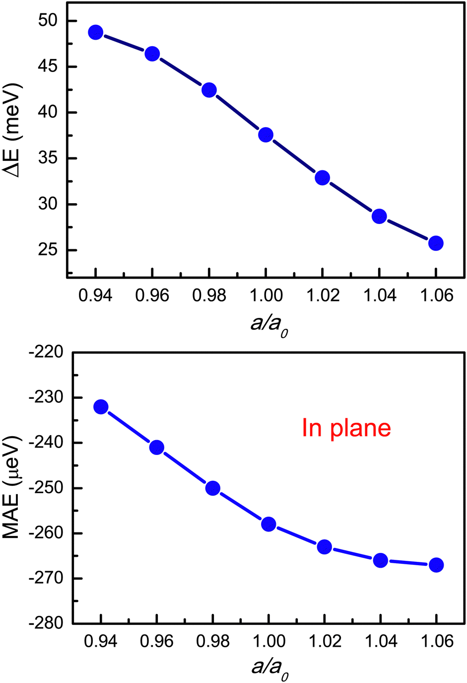 | ||
| Fig. 9 The energy differences ΔE between AFM and FM ordering and MAE as a function of a/a0. | ||
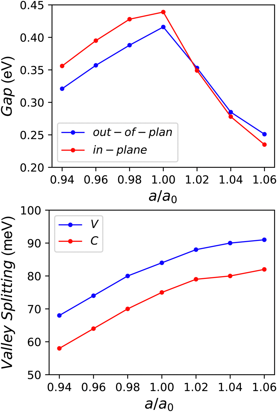 | ||
| Fig. 10 The gap (including out-of-plane and in-plane magnetic anisotropy) and valley splitting (including bottom conduction (C) and top valence (V) bands) as a function of a/a0. | ||
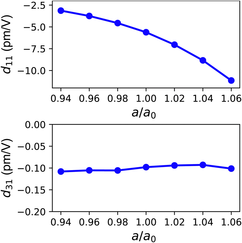
Next, the strain influences on the piezoelectric properties of YBrI are investigated. The elastic constants (C11, C12, C11 − C12 and C11 + C12) and piezoelectric stress coefficients (e11 and e31) along the ionic and electronic contributions vs. a/a0 are plotted in Fig. 5 and 6 of the ESI.† The d11/d31 values as a function of a/a0 are plotted in Fig. 11. It is found that increasing tensile strain can improve d11 (absolute value) due to decreased C11 − C12 and enhanced e11 based on pe2. At 1.06 strain, the d11 (−11.14 pm V−1) is about two times as large as an unstrained one (−5.61 pm V−1). So, strain is an effective way to tune the in-plane piezoelectric properties of YBrI. However, the strain has a weak influence on d31. In the considered strain range, the strained YBrI monolayer is mechanically stable, because the calculated elastic constants (Fig. 5 of the ESI†) satisfy the mechanical stability criteria.
 | ||
| Fig. 11 The piezoelectric strain coefficient d11 and d31 as a function of a/a0. | ||
7 Magnetic transition temperature
Within U and a/a0 ranges, the calculated MAE shows that the YBrI monolayer prefers in-plane easy magnetization, implying that there is no energetic barrier to the rotation of magnetization in the xy plane.53 So, the YBrI should be a 2D XY magnet,53,54 and the monte Carlo simulations have shown that a Berezinskii–Kosterlitz–Thouless magnetic transition to a quasi-long-range phase could take place at a critical temperature ,55,56 where J and KB are the nearest-neighboring exchange parameter and Boltzmann constant. The J is determined from the energy difference between AFM (EAFM) and FM (EFM) orderings with a rectangle supercell. Based on the FM and AFM configurations, the FM and AFM energies can be obtained by equations:
| EFM = E0 − 6JS2 | (9) |
| EAFM = E0 + 2JS2 | (10) |
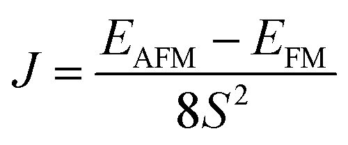 | (11) |
The critical temperature as a function of U and a/a0 (U = 2.0 eV) are plotted in Fig. 12. It is found that increasing electronic correlation and compressive strain can improve the TC of YBrI. The predicted TC of YBrI is higher than those of the experimentally discovered 2D ferromagnetic materials CrI3 (45 K) and Cr2Ge2Te6 (30 K).6,7
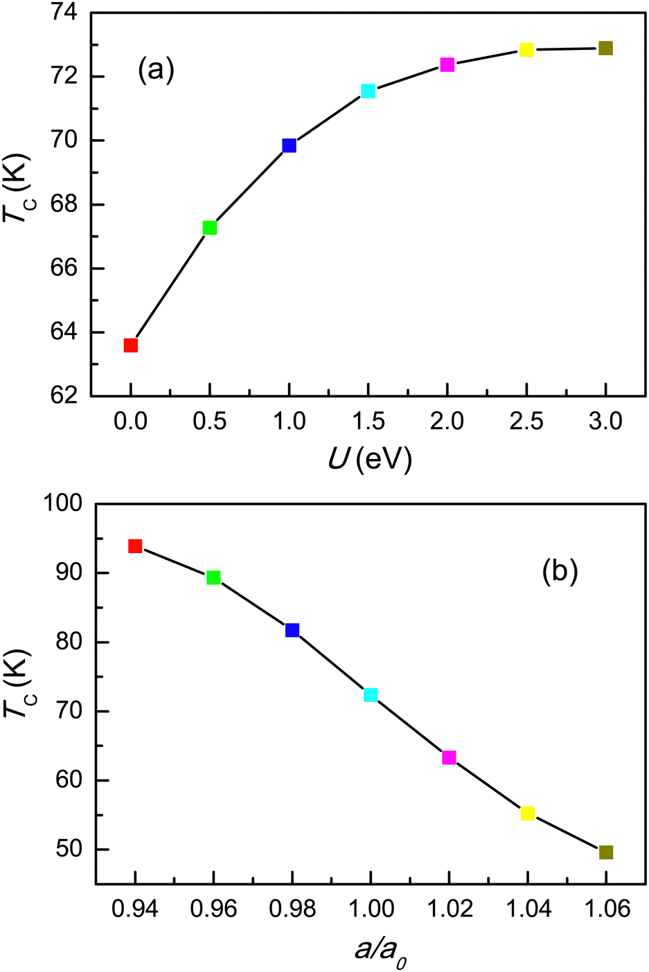 | ||
| Fig. 12 The critical temperature as a function of U (a) and a/a0 (b) at U = 2.0 eV. | ||
8 Discussion and conclusion
For many cases, the Heyd–Scuseria–Ernzerhof (HSE06) hybrid functional57 did give a better estimation of the band gap values for semiconductors, but there is no guarantee that the HSE06 result is always more accurate than the GGA result. For monolayer MoS2, the local-density approximation (LDA) gap of 1.86 eV is very close to the experimental value of 1.9 eV. The GGA gaps of monolayer MoSe2 (1.44 eV) and WSe2 (1.56 eV) are very close to the experimental values of MoSe2 (1.55 eV) and WSe2 (1.64 eV).58 Here, we also use HSE06 + SOC to calculate the energy bands of YBrI with the out-of-plane case, which is plotted in Fig. 7 of the ESI.† The HSE06 gap is improved to 803 meV from the GGA gap of 246 meV, but their band structures are similar. The YBrI monolayer has similar structures to MoS2, so the GGA+U method may be better than HSE06.YM2 (M = I, Br and Cl) monolayers have been predicted to be dynamically and thermally stable 2D FM semiconductors.18 Based on these monolayers, Janus YClBr and YClI monolayers can also be constructed, which should be FM and piezoelectric. Except for piezoelectric properties, the main analysis and results about YBrI can be readily extended to monolayer YMN (M/N = Cl, Br and I). YM2 (M = I, Br and Cl) monolayers possess a reflection symmetry with respect to the central Y atomic plane, which requires that e31/d31 = 0. Their piezoelectric polarizations are confined along the in-plane armchair direction. However, for monolayer YMN (M/N = Cl, Br and I; M≠ N), both e11/d11 and e31/d31 are nonzero, which means that both in-plane (along the armchair direction) and vertical piezoelectric polarizations are allowed. However, qualitative results should be invariable with varied U for monolayer YMN (M/N = Cl, Br and I).
In summary, based on reliable DFT calculations, we systemically investigate the stability, and the electronic, magnetic and piezoelectric properties of a Janus YBrI monolayer. For out-of-plane magnetic anisotropy, spontaneous valley polarization can be observed with valley splitting larger than 82 meV in the considered U range. However, for in-plane magnetic anisotropy, YBrI is a common FM semiconductor without spontaneous valley polarization. The MAE calculations show that the intrinsic easy axis of YBrI is always in-plane with U from 0.0 eV to 3.0 eV. Both in-plane and out-of-plane piezoelectric polarizations can be observed due to broken horizontal mirror symmetry, and the predicted in-plane d11 is higher than/comparable with ones of many familiar 2D materials. The predicted TC is larger than the reported values for 2D CrI3 and Cr2Ge2Te6.6,7 It is found that strain engineering is a very effective way to tune the physical properties of YBrI. Our findings suggest that YBrI can have promising applications in multipurpose spintronic devices.
Conflicts of interest
There are no conflicts to declare.Acknowledgements
This work is supported by the Natural Science Basis Research Plan in Shaanxi Province of China (2021JM-456), the Nature Science Foundation of China (Grant No. 11974393) and the Strategic Priority Research Program of the Chinese Academy of Sciences (Grant No. XDB33020100). We are grateful to the Shanxi Supercomputing Center of China, and the calculations were performed on TianHe-2.References
- A. Fert, Rev. Mod. Phys., 2008, 80, 1517 CrossRef CAS.
- M. N. Blonsky, H. L. Zhuang, A. K. Singh and R. G. Hennig, ACS Nano, 2015, 9, 9885 CrossRef CAS PubMed.
- K. N. Duerloo, M. T. Ong and E. J. Reed, J. Phys. Chem. Lett., 2012, 3, 2871 CrossRef CAS.
- W. Wu, L. Wang, Y. Li, F. Zhang, L. Lin, S. Niu, D. Chenet, X. Zhang, Y. Hao, T. F. Heinz, J. Hone and Z. L. Wang, Nature, 2014, 514, 470 CrossRef CAS PubMed.
- N. D. Mermin and H. Wagner, Phys. Rev. Lett., 1966, 17, 1133 CrossRef CAS.
- C. Gong, L. Li, Z. Li, H. Ji, A. Stern, Y. Xia and T. Cao, et al. , Nature, 2017, 546, 265 CrossRef CAS PubMed.
- B. Huang, G. Clark, E. Navarro-Moratalla, D. R. Klein, R. Cheng, K. L. Seyler and D. Zhong, et al. , Nature, 2017, 546, 270 CrossRef CAS PubMed.
- J. R. Schaibley, H. Yu, G. Clark, P. Rivera, J. S. Ross, K. L. Seyler, W. Yao and X. Xu, Nat. Rev. Mater., 2016, 1, 16055 CrossRef CAS.
- D. Xiao, G. B. Liu, W. Feng, X. Xu and W. Yao, Phys. Rev. Lett., 2012, 108, 196802 CrossRef PubMed.
- W. Y. Tong, S. J. Gong, X. Wan and C. G. Duan, Nat. Commun., 2016, 7, 13612 CrossRef CAS PubMed.
- P. Lin, C. Pan and Z. L. Wang, Mater. Today Nano, 2018, 4, 17 CrossRef.
- G. Song, D. S. Li and H. F. Zhou, et al. , Appl. Phys. Lett., 2021, 118, 123102 CrossRef CAS.
- S. D. Guo, W. Q. Mu, Y. T. Zhu and X. Q. Chen, Phys. Chem. Chem. Phys., 2020, 22, 28359 RSC.
- S. D. Guo, X. S. Guo, X. X. Cai, W. Q. Mu and W. C. Ren, J. Appl. Phys., 2021, 129, 214301 CrossRef CAS.
- J. H. Yang, A. P. Wang, S. Z. Zhang, J. Liu, Z. C. Zhong and L. Chen, Phys. Chem. Chem. Phys., 2019, 21, 132 RSC.
- S. D. Guo, J. X. Zhu, W. Q. Mu and B. G. Liu, Phys. Rev. B, 2021, 104, 224428 CrossRef CAS.
- Y. F. Zhao, Y. H. Shen, H. Hu, W. Y. Tong and C. G. Duan, Phys. Rev. B, 2021, 103, 115124 CrossRef CAS.
- W. Y. Liu, B. Huang, X. C. Wu, S. Z. Li, H. X. Li, Z. X. Yang and W. B. Zhang, arXiv, 2022, preprint, arXiv:2202.07850 DOI:10.48550/arXiv.2202.07850.
- S. Li, Q. Q. Wang, C. M. Zhang, P. Guo and S. A. Yang, Phys. Rev. B, 2021, 104, 085149 CrossRef CAS.
- S. D. Guo, J. X. Zhu, M. Y. Yin and B. G. Liu, Phys. Rev. B, 2022, 105, 104416 CrossRef CAS.
- S. D. Guo, W.-Q. Mu, J.-H. Wang, Y.-X. Yang, B. Wang and Y.-S. Ang, Phys. Rev. B, 2022, 106, 064416 CrossRef CAS.
- S. D. Guo, W. Q. Mu and B. G. Liu, 2D Mater., 2022, 9, 035011 CrossRef.
- S. Jiang, S. Nazir and K. Yang, Phys. Rev. B, 2020, 101, 134405 CrossRef CAS.
- S. Nazir and K. Yang, J. Phys.: Condens. Matter, 2022, 34, 214009 CrossRef PubMed.
- P. Hohenberg and W. Kohn, Phys. Rev., 1964, 136, B864 CrossRef.
- W. Kohn and L. J. Sham, Phys. Rev., 1965, 140, A1133 CrossRef.
- G. Kresse, J. Non-Cryst. Solids, 1995, 193, 222 CrossRef.
- G. Kresse and J. Furthmüller, Comput. Mater. Sci., 1996, 15, 15 CrossRef.
- G. Kresse and D. Joubert, Phys. Rev. B: Condens. Matter Mater. Phys., 1999, 59, 1758 CrossRef CAS.
- J. P. Perdew, K. Burke and M. Ernzerhof, Phys. Rev. Lett., 1996, 77, 3865 CrossRef CAS PubMed.
- S. L. Dudarev, G. A. Botton, S. Y. Savrasov, C. J. Humphreys and A. P. Sutton, Phys. Rev. B: Condens. Matter Mater. Phys., 1998, 57, 1505 CrossRef CAS.
- A. Togo, F. Oba and I. Tanaka, Phys. Rev. B: Condens. Matter Mater. Phys., 2008, 78, 134106 CrossRef.
- T. Fukui, Y. Hatsugai and H. Suzuki, J. Phys. Soc. Jpn., 2005, 74, 1674 CrossRef CAS.
- H. J. Kim, https://github.com/Infant83/VASPBERRY, (2018).
- H. J. Kim, C. Li, J. Feng, J.-H. Cho and Z. Zhang, Phys. Rev. B, 2016, 93, 041404 CrossRef.
- X. Wu, D. Vanderbilt and D. R. Hamann, Phys. Rev. B: Condens. Matter Mater. Phys., 2005, 72, 035105 CrossRef.
- A. Y. Lu, H. Zhu, J. Xiao, C. P. Chuu, Y. Han, M. H. Chiu, C. C. Cheng, C. W. Yang, K. H. Wei, Y. Yang, Y. Wang, D. Sokaras, D. Nordlund, P. Yang, D. A. Muller, M. Y. Chou, X. Zhang and L. J. Li, Nat. Nanotechnol., 2017, 12, 744 CrossRef CAS PubMed.
- J. Zhang, S. Jia, I. Kholmanov, L. Dong, D. Er, W. Chen, H. Guo, Z. Jin, V. B. Shenoy, L. Shi and J. Lou, ACS Nano, 2017, 11, 8192 CrossRef CAS PubMed.
- S. Faiza-Rubab, S. Naseem, S. Muhammad Alay-e-Abbas, M. Zulfiqar, Y. Zhao and S. Nazir, Phys. Chem. Chem. Phys., 2021, 23, 19472 RSC.
- S. Muhammad Alay-e-Abbas, S. Nazir, N. A. Noor, N. Amin and A. Shaukat, J. Phys. Chem. C, 2014, 118, 19625 CrossRef.
- R. C. Andrew, R. E. Mapasha, A. M. Ukpong and N. Chetty, Phys. Rev. B: Condens. Matter Mater. Phys., 2012, 85, 125428 CrossRef.
- J. Zhou, Y. P. Feng and L. Shen, Phys. Rev. B, 2020, 102, 180407 CrossRef CAS.
- P. Zhao, Y. Ma, C. Lei, H. Wang, B. Huang and Y. Dai, Appl. Phys. Lett., 2019, 115, 261605 CrossRef.
- X. Y. Feng, X. L. Xu, Z. L. He, R. Peng, Y. Dai, B. B. Huang and Y. D. Ma, Phys. Rev. B, 2021, 104, 075421 CrossRef CAS.
- P. Zhao, Y. Dai, H. Wang, B. B. Huang and Y. D. Ma, Chem. Phys. Mater., 2022, 1, 56 Search PubMed.
- R. Li, J. W. Jiang, W. B. Mi and H. L. Bai, Nanoscale, 2021, 13, 14807 RSC.
- D. Xiao, M. C. Chang and Q. Niu, Rev. Mod. Phys., 2010, 82, 1959 CrossRef CAS.
- L. Dong, J. Lou and V. B. Shenoy, ACS Nano, 2017, 11, 8242 CrossRef CAS PubMed.
- E. Scalise, M. Houssa, G. Pourtois, V. Afanas'ev and A. Stesmans, Nano Res., 2012, 5, 43 CrossRef CAS.
- H. K. Liu, G. Z. Qin, Y. Lin and M. Hu, Nano Lett., 2016, 16, 3831 CrossRef CAS PubMed.
- H. Huan, Y. Xue, B. Zhao, G. Y. Gao, H. R. Bao and Z. Q. Yang, Phys. Rev. B, 2021, 104, 165427 CrossRef CAS.
- L. Huang, F. G. Wu and J. B. Li, J. Chem. Phys., 2016, 144, 114708 CrossRef PubMed.
- K. Sheng, Q. Chen, H. K. Yuan and Z. Y. Wang, Phys. Rev. B, 2022, 105, 075304 CrossRef CAS.
- J. L. Lado and J. Fernández-Rossier, 2D Mater., 2017, 4, 035002 CrossRef.
- P. Jiang, L. Kang, Y.-L. Li, X. Zheng, Z. Zeng and S. Sanvito, Phys. Rev. B, 2021, 104, 035430 CrossRef CAS.
- S. Zhang, R. Xu, W. Duan and X. Zou, Adv. Funct. Mater., 2019, 29, 1808380 CrossRef.
- J. Heyd, G. E. Scuseria and M. Ernzerhof, J. Chem. Phys., 2013, 118, 8207 CrossRef.
- S. Kumar and U. Schwingenschlögl, Chem. Mater., 2015, 27, 1278 CrossRef CAS.
Footnote |
| † Electronic supplementary information (ESI) available: Electronic, elastic, and piezoelectric properties of YBrI as a function of U or a/a0. See DOI: https://doi.org/10.1039/d2cp05046c |
| This journal is © the Owner Societies 2023 |