
An ultra-broadband and wide-angle absorber based on a TiN metamaterial for solar harvesting
Chunlei
Sun
a,
Haotuo
Liu
bc,
Bing
Yang
d,
Kaihua
Zhang
e,
Bin
Zhang
*a and
Xiaohu
Wu
 *b
*b
aCollege of Electromechanical Engineering, Qingdao University of Science and Technology, Qingdao 266061, China. E-mail: zb-sh@163.com
bShandong Institute of Advanced Technology, Jinan 250100, China. E-mail: xiaohu.wu@iat.cn
cSchool of Energy Science and Engineering, Harbin Institute of Technology, Harbin 150001, China
dCentre for Advanced Laser Manufacturing (CALM), School of Mechanical Engineering, Shandong University of Technology, Zibo 255000, China
eHenan Key Laboratory of Infrared Materials & Spectrum Measures and Applications, School of Physics, Henan Normal University, Xinxiang 453007, China
First published on 1st December 2022
Abstract
The efficient absorption of solar spectrum radiation is the most critical step in solar thermal utilization. In this work, a near-perfect metamaterial solar absorber with broadband, wide angle, polarization insensitivity, and high-temperature resistance is proposed and investigated. The absorber takes advantage of the high melting point material, which consists of a TiN reflector, a SiO2 insulating layer, and a TiN ring array. In the spectral range of 300–2500 nm, an average absorption of 97.6% is achieved. The percentage of absorbed energy in the AM1.5 spectral radiation can reach 95.8%. The electric and magnetic field distributions show that the high absorption is attributed to the coupling effect of surface plasmon resonance, guided mode resonance and cavity resonance. Furthermore, the absorber is found to maintain high absorption performance at large angles of solar radiation and to be insensitive to polarization. The designed absorber maintains its broadband absorption performance well within certain geometric tolerances. This reduces the complexity and cost of manufacturing and facilitates practical applications. The research indicates that this work will benefit the design and application of solar thermal conversion and thermophotovoltaic systems.
1. Introduction
The energy crisis is an important factor limiting economic and social development, and the development of renewable energy is the main way to solve this problem. Solar energy, as an inexhaustible source of clean energy should be the pioneer in alleviating the energy crisis. In the utilization of solar energy, whether it is photothermal or photoelectric conversion, the efficient collection of solar energy is its prerequisite. This requires the development of solar absorbers that can absorb solar energy efficiently and are resistant to high temperatures.A metamaterial is an artificial material consisting of metallic and dielectric subwavelength structures arranged in a periodic array,1,2 which has extraordinary electromagnetic properties not possessed by natural materials. Metamaterial perfect absorbers (MPAs) have been extensively studied in the past few years since they were first reported by Landy et al.3 It has been developed in numerous fields, including solar cells,4,5 plasma sensors,6–8 detectors,9,10 radiothermometers,11,12 thermal emitters,13,14 and imaging devices.15–17 By changing the structural parameters of the absorbers, the effective permittivity and permeability of the structural material can be adjusted to match the impedance with the incident medium, thus achieving perfect absorption of light.18–20 Ideally, solar absorbers provide perfect absorption of solar radiation.
So far, various structures of solar absorbers have been proposed by scholars for the solar radiation spectrum.21–24 Zhong et al.25 proposed a semi-cylindrical cavity structure absorber based on refractory materials. The average absorption in the visible region is up to 94%. Liu et al.26 designed an ultrathin two-dimensional cylindrical array metamaterial absorber composed of TiN and TiO2. The spectral absorption of this absorber can reach more than 90% in the 316–1426 nm band. Obaidullah et al.27 proposed a metamaterial absorber based on vertical single-walled carbon nanotubes compounded with silicon dielectric materials. The absorber is simple in structure, easy to manufacture, and capable of almost complete absorption in the visible and ultraviolet regions with varying geometric parameters. However, the enhanced absorption is limited to a narrow bandwidth of visible wavelengths, and the single-walled carbon nanotubes increase the fabrication cost of the absorber. To further improve the absorption in the near-infrared region, Patel et al.28 designed a metamaterial absorber consisting of a phi-shaped resonator based on silver metal, a SiO2 substrate, and a silver metal ground layer. The absorber achieves an average absorbance of 94.42% in the ultraviolet to the mid-infrared range, achieving ultra-broadband characteristics. Wu et al.29 designed a stacked ring structure absorber using Ti, TiN, and Si3N4. The study showed that the absorber achieves an absorption efficiency of more than 90% and an absorption bandwidth of more than 2450 nm for the purpose of broadening the absorption band. Liu et al.30 also proposed a laminated ring structure absorber consisting of discs of different radii. An average absorption of 91% is achieved in the 250–4000 nm band. Jiang et al.31 designed a disc array absorber using GaAs, Ti, and metallic tungsten (W), which can achieve ultra-broadband, near-perfect solar absorption. The strong absorption of the MPAs mainly comes from impedance matching and coupling resonance.32,33 Although the above MPAs have excellent absorption properties, they still have the disadvantages of a complex structure and high manufacturing cost, which inevitably hinder their potential application prospects.
In this work, we propose and investigate a polarization-independent, broadband, wide-angle, high-temperature tolerant near-perfect solar absorber. The absorber consists of a TiN substrate reflector, an insulating layer of the SiO2 film, and an array of TiN rings. The spectral absorption performance of the absorber is investigated using the finite difference time domain (FDTD) method. The physical mechanism of the high absorption performance of this absorber is revealed by the calculated electric and magnetic field distributions. The effect of geometric manufacturing tolerances on the spectral absorption performance of the absorber is considered. The effect of the randomness of the incident angle and polarization angle of sunlight on the absorption spectrum is further analyzed. The solar absorption ratio under AM1.5 spectral radiation is also analyzed to assess the absorber's solar energy harvesting potential. This work will contribute to the design of devices such as solar collectors and solar cells.
2. Design and methods
Due to the plasmon resonance and optical coupling properties noble metals are often used as ideal absorber materials. However, most noble metals suffer from short absorption spectra and are also subject to problems such as high cost.34Fig. 1(a) shows the structure of the proposed metamaterial solar absorber, consisting of a TiN substrate reflector, a SiO2 film, and a TiN ring array. TiN is considered as a substitute for the precious metal gold35 and can operate in complex electromagnetic environments and under high-temperature conditions. TiN has a melting point of about 3200 K, and the melting point of SiO2 is about 1900 K. The high thermal stability and rather low ohmic thermal effect of TiN can be advantageous during high energy operation.36 In contrast to the common absorber formed by metallic nano-resonant cavities, TiN-based solar absorbers have greater thermal stability.25 The metamaterial absorber has the first layer of periodic ring arrays that match impedance and reduce light reflection. The period of the ring arrays is L, and d and D are the inner and outer diameters of the rings, respectively, and h1 is the height of the ring arrays. The SiO2 layer is designed to allow electromagnetic waves to pass through, with h2 being its height. The TiN substrate blocks the electromagnetic radiation, so the transmittance remains zero. θ is the angle at which the TE or TM wave is incident on the surface of the structure. The refractive index of SiO2 is 1.45. The optical parameters of TiN are taken from ref. 37, and the complex refractive index is shown in Fig. 2. The real part n is the refractive index of the absorbing medium and depends on the propagation speed of the light wave in the absorbing medium. The imaginary part k depends on the attenuation of the light wave as it propagates in the absorbing medium. To obtain a better solar absorber, the structural parameters are taken as h1 = 290 nm, h2 = 60 nm, d = 260 nm, D = 290 nm, and L = 430 nm after repeated calculations.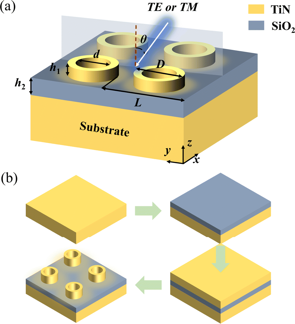 | ||
| Fig. 1 (a) The proposed metamaterial absorber structure, which consists of a TiN reflector, a SiO2 dielectric film, and a TiN ring array. (b) Simple preparation flow chart of the absorber. | ||
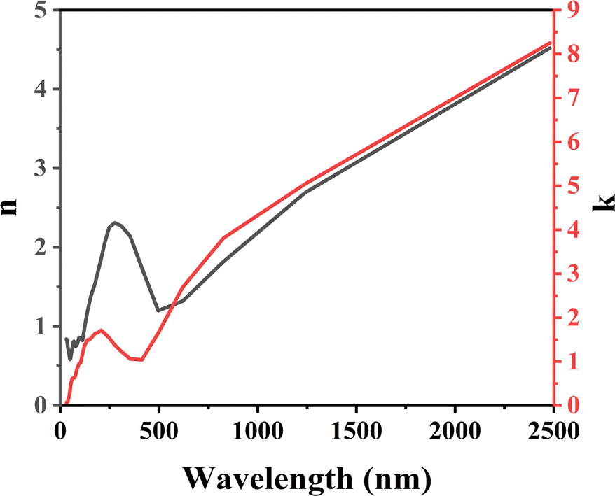 | ||
| Fig. 2 Real and imaginary parts of the TiN complex refractive index taken from ref. 37. | ||
The general flow chart of the preparation of the metamaterial solar absorber is shown in Fig. 1(b). Ultrasonic cleaning of the TiN substrate and the use of ion beam sputtering allow the placement of a SiO2 film on the TiN substrate. A TiN film is then deposited using magnetron sputtering. Finally, the final microstructure is fabricated using photolithography and electron beam evaporation.38 In this work, the spectral absorption performance of the solar absorber is investigated using Lumerical commercial software based on the FDTD method. The light source is a plane wave, which is incident vertically along the z-axis onto the absorber. The wavelength range is taken as 300–2500 nm. The x and y directions are periodic boundary conditions, and the perfect matching layers are used in the z-direction. The Bloch boundary condition is used for oblique incidence. A reflectivity monitor (R) is set in the upper part of the ring arrays. A transmittance monitor (T) is set in the lower part of the substrate, where the transmittance is 0 due to the large thickness of the TiN reflector. The working environment of the absorber is air. The absorption rate can be expressed as:
| A(λ) = 1 − R(λ), | (1) |
To evaluate the ability of this solar absorber to collect solar energy, the solar spectral absorption ratio under standard AM1.5 spectral39 radiation at positive solar incidence can be expressed as:34
| Iabs(λ) = A(λ)·Is(λ), | (2) |
| ILoss(λ) = Is(λ) − Iabs(λ), | (3) |
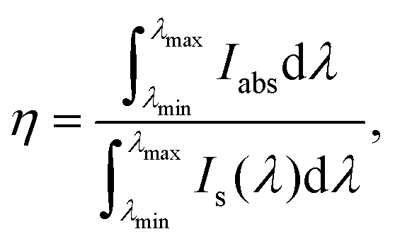 | (4) |
3. Results and discussion
The spectral absorbance of the absorber in the 300–2500 nm band is shown in Fig. 3. One can see that the absorber has good broadband absorption performance in this spectral range, with an average absorption of up to 97.6%. Periodic TiN ring arrays match impedance and reduce light reflection, enhancing light collection across the nearly full solar spectrum. In addition, four absorption peaks are shown near 330 nm, 475 nm, 970 nm, and 2140 nm. The absorption values are 98.2%, 97.7%, 99.4% and 99.9%, respectively.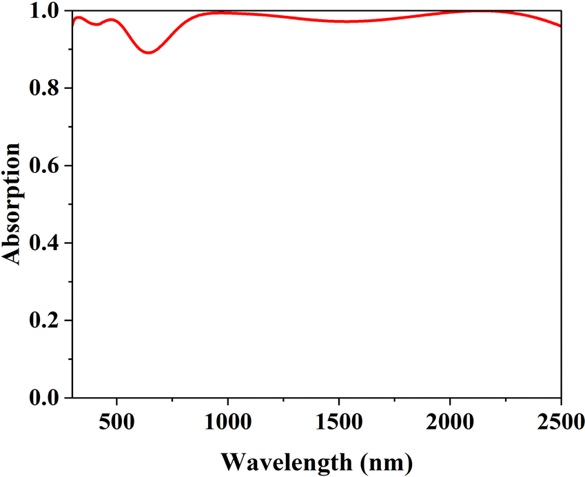 | ||
| Fig. 3 Spectral absorption of the metamaterial absorber in 300–2500 nm at normal incidence for TM polarization. | ||
The strong absorption of plasmonic absorbers mainly results from the excitation of different plasmonic resonance modes at the metal/dielectric interface.40 The physical mechanism of the broadband absorption performance of the absorber is revealed below. The normalized electric field distribution at the wavelength corresponding to the absorption peak is shown in Fig. 4. The collision of electrons with TiN nano-resonant cavities under the action of a local electric field can produce high-energy electrons.38 As shown in Fig. 4(a), the upper half of the TiN array produced surface plasmon resonance (SPR). Fig. 4(e) shows the top view of the corresponding normalized electric field. The thickness of the ring structure is very thin so that the surface plasmons generated by the inner and outer rings can couple with each other. This phenomenon leads to a significant enhancement of the electric field inside and outside the ring. Combined with the magnetic field distribution in Fig. 5(a), the apparent stationary waves within the TiN ring's air gap exhibit the typical characteristics of guided mode resonance (GMR). Thus, the high absorption achieved at 330 nm can be attributed to the effect of SPR and GMR coupling excited by the TiN ring arrays. Fig. 4(b) shows the electric field distribution at 475 nm. Combining the electric field distribution and the corresponding magnetic field distribution in Fig. 5(b), we find that the typical features of GMR are exhibited in the air gap of the TiN ring. Moreover, the top view of the electric field at 475 nm (Fig. 4(f)) shows that the electric field inside the ring is significantly enhanced due to the cavity resonance (CR). Thus, the high absorption performance at 475 nm can be attributed to GMR and CR. The electric field distribution at the absorption peak of 970 nm is shown in Fig. 4(c) and (g), and the magnetic field distribution is shown in Fig. 5(c). Besides the SPR excited by the TiN ring, strong cavity resonance (CR) also appears. The normalized electric field distribution at the absorption peak at 2140 nm is shown in Fig. 4(d) and (h). The top-view of electric field distribution is exactly opposite to that at 970 nm. The magnetic field distribution in Fig. 5(d) shows that the resonance mode here can still be attributed to the coupling of GMR and CR. The coupling of different resonance modes at 970 nm and 2140 nm leads to a significant enhancement of broadband absorption in the near-infrared band. One can see that the strong broadband absorption performance of this absorber is due to the mutual coupling between SPR, GMR and CR.
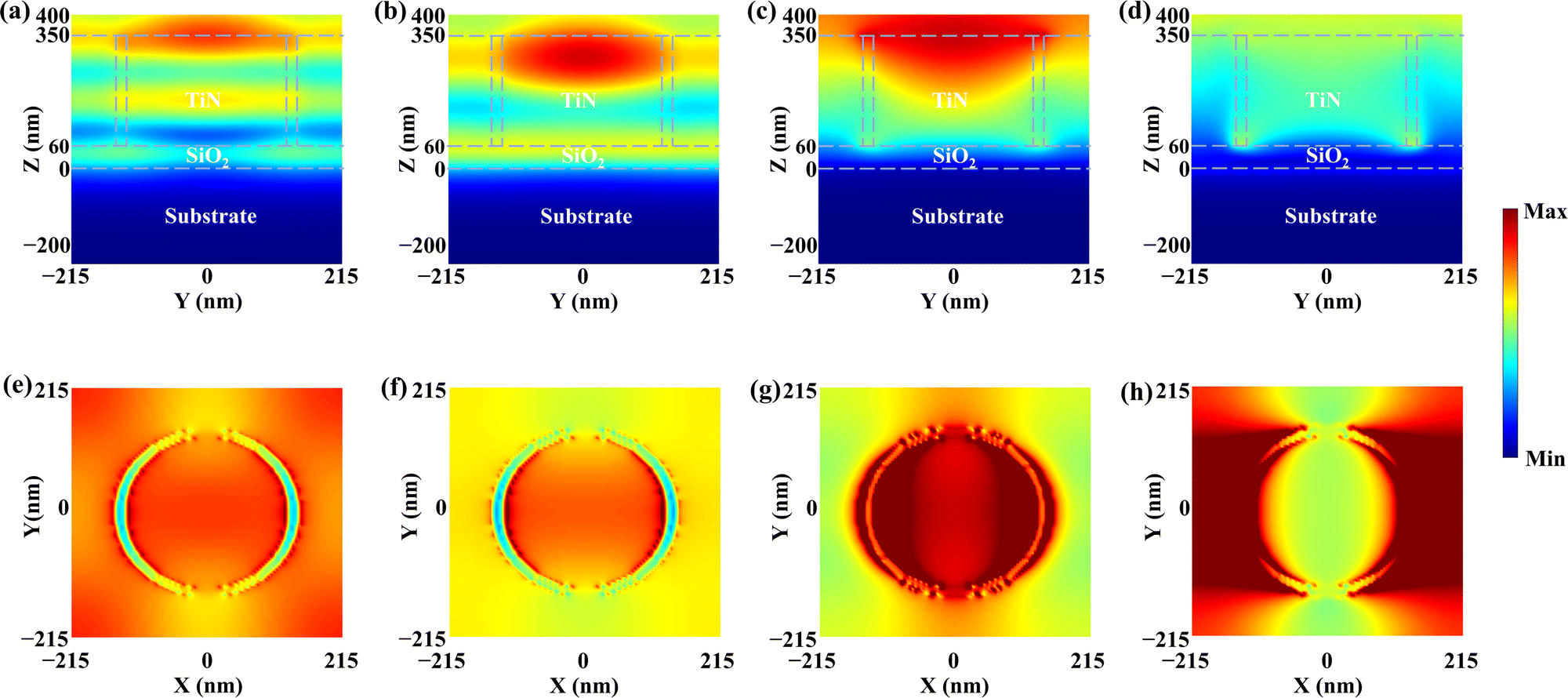 | ||
| Fig. 4 The side-views of electric field distribution |E/E0| at (a) 330 nm, (b) 475 nm, (c) 970 nm and (d) 2140 nm and the top-views of electric field distribution |E/E0| at (e) 330 nm, (f) 475 nm, (g) 970 nm and (h) 2140 nm. | ||
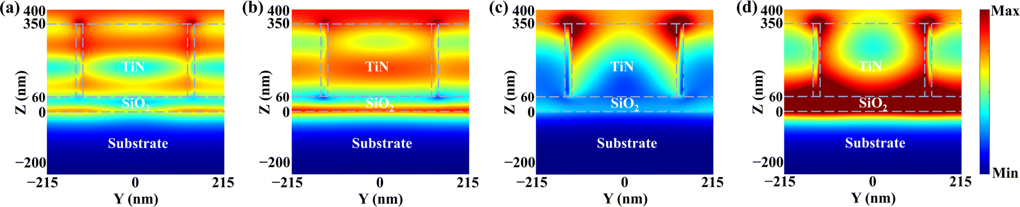 | ||
| Fig. 5 The side-views of magnetic field distribution |H/H0| at (a) 330 nm, (b) 475 nm, (c) 970 nm and (d) 2140 nm. | ||
The geometrical parameters of the absorber can have an important effect on its spectral absorption performance.41–43 The effect of geometry on the absorption performance of the absorber is discussed by the controlled variable method as shown in Fig. 6. Here, the absorption characteristics of the absorber are analyzed by varying each parameter individually, keeping the other parameters constant.
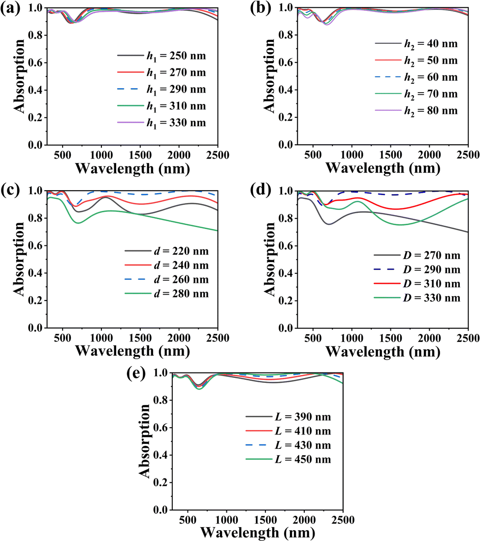 | ||
| Fig. 6 Effect of structural parameters on the spectral absorbance of (a) TiN ring array height h1, (b) dielectric layer SiO2 thickness h2, (c) ring inner diameter d, (d) ring outer diameter D and (e) ring array period L. | ||
Fig. 6(a) shows the effect of the height h1 of the periodic TiN ring array on the absorption performance. One can see that the spectral absorption curve does not undergo large fluctuations with the change of h1. As h1 increases, all four absorption peaks undergo a slight red shift, which is favorable for broadening the absorption spectrum of solar energy. The absorption intensities of the first, second and fourth absorption peaks are slightly enhanced, while that of the third absorption peak is reduced. Fig. 6(b) shows the effect of the dielectric layer SiO2 thickness h2. It is easy to see that the thickness of SiO2 also satisfies certain geometrical manufacturing tolerances. With the increase of h2, the absorption spectrum is red-shifted. The intensities of the first, second and third absorption peaks are decreased, and the intensity of the fourth absorption peak is increased. It is obvious from Fig. 6(c) and (d) that the inner diameter d and outer diameter D of the TiN ring array have a large effect on the spectral absorption performance. However, the results show that the absorber maintains a spectral absorption performance of nearly 80% despite such a large fabrication work difference. Also, it can be seen from Fig. 6(e) that the ring array period L has little effect on the spectral absorption performance. It shows that the absorber is manufactured to meet certain geometric tolerances and is highly operable in practical applications.
The light source usually cannot be incident vertically on the device. In practical applications, the design of the absorber has to take into account the influence of the angle of incidence of solar energy. Therefore, it is necessary to investigate solar absorbers that are highly inclusive of the light incidence angle. The spectral absorption performance of the absorber when the TM wave is incident at different angles θ is given in Fig. 7(a). It is obvious that the absorber has a high spectral absorption for different sunlight incidence angles. The average spectral absorbance of 84% is maintained even when the angle of incidence reaches 70°. The average absorption rate of 91.8% can be maintained at an incidence angle of 55°. Due to the in-plane symmetry of the structure, the absorption performance under TE wave incidence exhibits similar results to that of TM wave incidence. Fig. 7(b) shows the spectral absorption performance of the absorber when the TE wave is incident at different angles θ. The average spectral absorption is 80.6% when the incidence angle is 70°. This is because the effective dielectric constant of the waveguide layer gradually decreases as the incident angle increases, resulting in a blue shift in the absorption band.38,44,45 It shows that the absorber has a large angular sensitivity. Fig. 7(c) shows the effect of plane wave polarization angle on the spectral absorption performance of the absorber at normal incidence. One can see that the absorption spectrum of the absorber is independent of the polarization angle. This phenomenon is caused by the structural symmetry of this metamaterial absorber.46 SPR can be affected by polarization.47 An axisymmetric subwavelength structure that is insensitive to polarization will significantly improve the SPR,48,49 so this absorber structure usually yields good results.
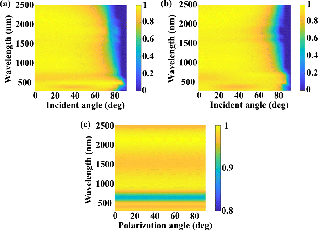 | ||
| Fig. 7 The spectral absorbance versus wavelength and incidence angle for (a) TE polarization and (b) TM polarization. (c) The spectral absorbance versus wavelength and polarization angle at normal incidence. | ||
The proposed metamaterial absorber is mainly focused on the collection of solar energy. To further evaluate the solar energy harvesting capacity of the absorber, the energy absorption ratio η of the designed absorber is calculated in combination with the AM1.5 radiation spectrum. Fig. 8 shows the AM1.5 radiation spectrum Is, the absorption spectrum Iabs of this absorber, and the loss solar spectrum ILoss. The percentage of absorbed energy in the visible band (390–780 nm) is about 93.9%. The percentage of absorbed energy in the near-infrared band (780–2500 nm) is 95.7%. The spectral absorption efficiency of this solar absorber is 95.8%, obtained by eqn (2)–(4). The results show that the absorber loses only 4.2% of the solar energy, again proving that the designed absorber has a good solar harvesting capability.
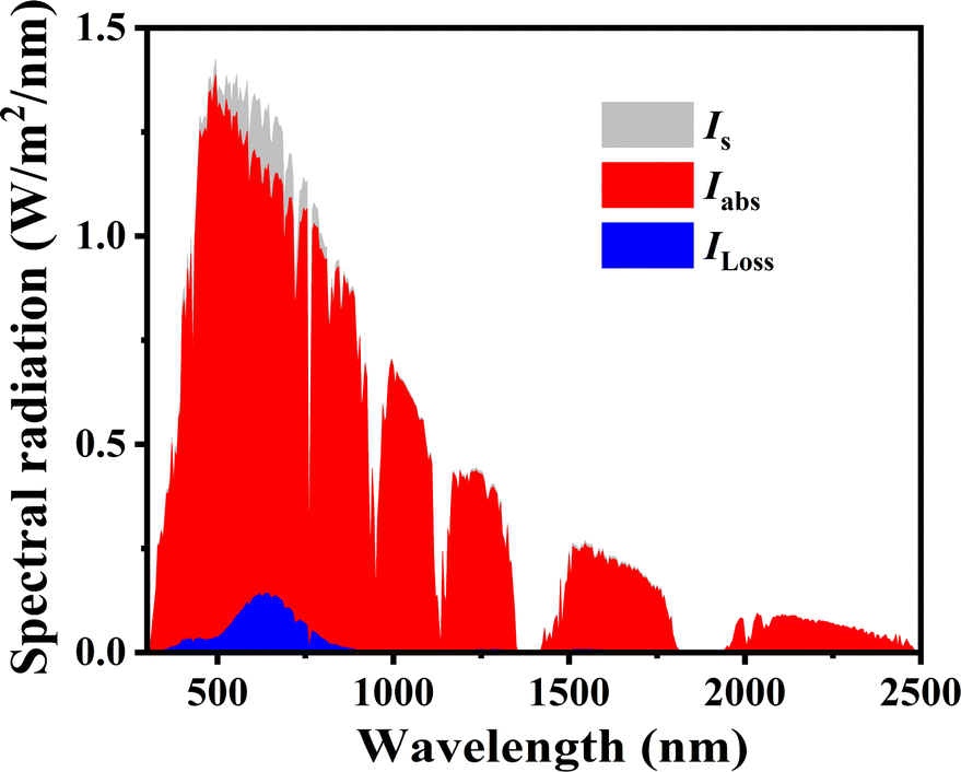 | ||
| Fig. 8 Spectral absorption characteristics of the absorber in the AM1.5 solar radiation spectrum. | ||
4. Conclusions
In conclusion, we provide a novel and feasible way to realize full-spectrum, near perfect, subwavelength-scale solar absorbers. The proposed solar absorber has absorption bandwidth, polarization insensitivity, wide angle, and high-temperature resistance. The average absorption in the 300–2500 nm band can reach 97.6%. By changing the size structure of the absorber, it is found that the absorber has a certain geometric manufacturing difference, which also has some advantages for practical application in manufacturing. The analysis of the electric and magnetic field distributions reveals that the physical mechanism of the high absorption is the coupling effect of SPR, GMR, and CR. The absorber still maintains more than 80% of the average spectral absorption when the incidence angle is 70°. Moreover, the absorber can achieve an energy absorption ratio of 95.8% in the AM1.5 radiation spectrum, showing a good solar energy collection capability. We believe that this work will have a significant impact on the design and application of solar collectors and thermophotovoltaics.Author contributions
Funding acquisition, X. H. Wu; methodology, C. L. Sun. and H. T. Liu; supervision, B. Yang, B. Zhang and X. H. Wu; writing – original draft, C. L. Sun and H. T. Liu; writing – review and editing, K. H. Zhang, B. Zhang and X. H. Wu. All authors have read and agreed to the published version of the manuscript.Conflicts of interest
The authors declare no conflict of interest.Acknowledgements
This work was supported by the National Natural Science Foundation of China (52106099) and the Shandong Provincial Natural Science Foundation (ZR2022YQ57).References
- Q. Q. Liang, T. S. Wang, Z. W. Lu, Q. Sun, Y. Q. Fu and W. X. Yu, Adv. Opt. Mater., 2013, 1, 43–49 CrossRef.
- H. Hajian, I. D. Rukhlenko, G. W. Hanson and E. Ozbay, Photonics Nanostruct. Fundam. Appl., 2022, 50, 101020 CrossRef.
- N. I. Landy, S. Sajuyigbe, J. J. Mock, D. R. Smith and W. Padilla, Phys. Rev. Lett., 2008, 100, 207402 CrossRef CAS PubMed.
- R. Kumar, B. K. Singh and P. C. Pandey, Phys. E, 2022, 142, 115327 CrossRef CAS.
- Y. Wang, T. Y. Sun, T. Paudel, Y. Zhang, Z. F. Ren and K. Kempa, Nano Lett., 2012, 12, 440–445 CrossRef CAS PubMed.
- S. Y. Li, X. C. Ai, R. H. Wu and J. J. Chen, Opt. Commun., 2018, 428, 251–257 CrossRef CAS.
- Y. Z. Cheng, F. Chen and H. Luo, Nanoscale Res. Lett., 2020, 15, 103 CrossRef CAS.
- Y. Z. Cheng, H. Luo, F. Chen and R. Z. Gong, OSA Continuum, 2019, 2, 2113–2122 CrossRef CAS.
- J. J. Bai, Z. Q. Pang, P. Y. Shen, T. T. Chen, W. Shen, S. S. Wang and S. J. Chang, Opt. Commun., 2021, 497, 127184 CrossRef CAS.
- J. F. Li, C. Zhao, B. Y. Liu, C. Y. You, F. H. Chu, N. Tian, Y. F. Chen, S. Y. Li, B. X. An, A. Cui, X. P. Zhang, H. Yan, D. M. Liu and Y. Z. Zhang, Appl. Surf. Sci., 2019, 473, 633–640 CrossRef CAS.
- A. Noor, Optik, 2022, 255, 168691 CrossRef.
- V. Savinov, V. A. Fedotov, P. A. J. de Groot and N. I. Zheludev, Supercond. Sci. Technol., 2013, 26, 084001 CrossRef CAS.
- B. H. Chen, S. Q. Shan, J. Z. Liu and Z. J. Zhou, Sol. Energy, 2022, 231, 194–202 CrossRef.
- Q. Liu, W. C. Wu, S. H. Lin, H. Xu, Y. H. Lu and W. J. Song, Opt. Commun., 2019, 450, 246–251 CrossRef CAS.
- J. W. Kim, G. Hwang, S. Lee, S. Kim and S. Wang, Mech. Syst. Signal Process, 2022, 179, 109374 CrossRef.
- Y. Z. Cheng, F. Chen and H. Luo, Nanoscale Res. Lett., 2021, 16, 12 CrossRef CAS PubMed.
- S. Lee, S. Shin, Y. Roh, S. J. Oh, S. H. Lee, H. S. Song, Y. Ryu, Y. K. Kim and M. Seo, Biosens. Bioelectron., 2020, 170, 112663 CrossRef CAS.
- J. Wu, Y. S. Sun, B. Y. Wu, C. L. Sun and X. H. Wu, Int. J. Therm. Sci., 2022, 179, 107638 CrossRef CAS.
- J. Wu, D. C. Huang, B. Y. Wu and X. H. Wu, Phys. Chem. Chem. Phys., 2022, 24, 21612–21616 RSC.
- H. T. Liu, M. Xie, Q. Ai and Z. H. Yu, J. Quant. Spectrosc. Radiat. Transfer, 2021, 266, 107575 CrossRef CAS.
- Y. Qiu, P. F. Zhang, Q. Li, Y. T. Zhang and W. H. Li, Sol. Energy, 2021, 230, 1165–1174 CAS.
- Q. Y. Qian, Y. Yan and C. Wang, Opt. Lett., 2018, 43, 312757 Search PubMed.
- E. M. Sheta, P. K. Choudhury and A. M. A. Ibrahim, Opt. Mater., 2022, 133, 112990 CrossRef CAS.
- P. H. Wu, K. H. Wei, D. Y. Xu, M. S. Chen, Y. X. Zeng and R. H. Jian, Nanomaterials, 2021, 11, 2040 CrossRef CAS PubMed.
- H. Z. Zhong, Z. Q. Liu, P. Tang, X. S. Liu, X. F. Zhan, P. P. Pan and C. J. Tang, Sol. Energy, 2020, 208, 445–450 CrossRef CAS.
- Z. Q. Liu, G. Q. Liu, Z. P. Huang, X. S. Liu and G. L. Fu, Sol. Energy Mater. Sol. Cells, 2018, 179, 346–352 CrossRef CAS.
- M. Obaidullah, V. Esat and C. Sabah, Opt. Laser Technol., 2021, 134, 106623 CrossRef CAS.
- S. K. Patel, J. Surve, P. Prajapati and S. A. Taya, Opt. Mater., 2022, 131, 112683 CrossRef CAS.
- P. J. Wu, S. F. Dai, X. T. Zeng, N. Su, L. N. Cui and H. S. Yang, Int. J. Therm. Sci., 2023, 183, 107890 CrossRef CAS.
- H. S. Zhang, Y. Z. Cheng and F. Chen, Optik, 2021, 229, 166300 CrossRef CAS.
- Z. R. Li, Y. Z. Cheng, H. Luo, F. Chen and X. C. Li, J. Alloys Compd., 2022, 925, 166617 CrossRef CAS.
- G. Q. Liu, X. S. Liu, J. Chen, Y. Y. Li, L. L. Shi, G. L. Fu and Z. Q. Liu, Sol. Energy Mater. Sol. Cells, 2019, 190, 20–29 CAS.
- J. B. Jiang, Y. P. Xu, Y. H. Li, L. Y. Ren, F. Chen, S. B. Cheng, W. X. Yang, C. J. Ma, Z. Y. Wang and X. W. Zhou, Optik, 2021, 246, 167855 CrossRef CAS.
- P. Q. Yu, H. Yang, X. F. Chen, Z. Yi, W. T. Yao, J. F. Chen, Y. G. Yi and P. H. Wu, Renewable Energy, 2020, 158, 227–235 CrossRef CAS.
- S. Ishii, R. Kamakura, H. Sakamoto, T. D. Dao, S. L. Shinde, T. Nagao, K. Fujita, K. Namura, M. Suzuki, S. Murai and K. Tanaka, Nanoscale, 2018, 10, 18451–18456 RSC.
- Z. Yang, S. Ishii, A. Doan, S. L. Shinde, T. D. Dao, Y. Lo, K. Chen and T. Nagao, Adv. Opt. Mater., 2020, 8, 1900982 CrossRef CAS.
- E. Palik, Handbook of Optical Constants of Solids, Academic Press, Cambridge, MA, USA, 1998 Search PubMed.
- F. Qin, X. F. Chen, Z. Yi, W. T. Yao, H. Yang, Y. J. Tang, Y. Yi, H. L. Li and Y. G. Yi, Sol. Energy Mater. Sol. Cells, 2020, 211, 110535 CrossRef CAS.
- Air Mass 1. Spectra, American society for testing and materials (ASTM). http://rredc.nrel.gov/solar/spectra/am1.5/.
- Y. Z. Cheng and C. Y. Du, Opt. Mater., 2019, 98, 109441 CrossRef CAS.
- Y. I. Abdulkarim, F. Alkurt, H. N. Awl, F. F. Muhammadsharif, M. Bakır, S. Dalgac, M. Karaaslan and H. Luo, Results Phys., 2021, 26, 104344 CrossRef.
- S. Mahmud, S. S. Islam, K. Mat, M. E. H. Chowdhury, H. Rmili and M. T. Islam, Results Phys., 2020, 18, 103259 CrossRef.
- Z. Y. Meng, H. L. Cao and X. D. Wu, Opt. Mater., 2019, 96, 109347 CrossRef CAS.
- H. Li, D. Wu, Y. M. Liu, C. Liu, J. Li, Z. H. Xu, L. Yang, Z. Y. Yu, L. Yu and H. Ye, J. Appl. Phys., 2018, 57, 110303 CrossRef.
- Z. X. Wu, Z. K. Ren, J. Wang, S. H. Hou, Y. J. Liu, Q. Zhang, J. Mao, X. J. Liu and F. Cao, Sol. Energy Mater. Sol. Cells, 2022, 238, 111582 CrossRef CAS.
- J. Wu, Y. Sun, B. Wu, C. Sun and X. Wu, Sol. Energy, 2022, 238, 78–83 CrossRef CAS.
- T. Søndergaard, S. M. Novikov, T. Holmgaard, R. L. Eriksen, J. Beermann, Z. Han, K. Pedersen and S. I. Bozhevolnyi, Nat. Commun., 2012, 3, 969 CrossRef PubMed.
- Y. P. Qi, Y. Zhang, C. Q. Liu, T. Zhang, B. H. Zhang, L. Y. Wang, X. Y. Deng, Y. L. Bai and X. X. Wang, Results Phys., 2020, 16, 103012 CrossRef.
- A. Moreau, C. Ciracì, J. J. Mock, R. T. Hill, Q. Wang, B. J. Wiley, A. Chilkoti and D. R. Smith, Nature, 2012, 492, 86–89 CrossRef CAS.
| This journal is © the Owner Societies 2023 |