
Photoabsorbance of supported metal clusters: ab initio density matrix and model studies of large Ag clusters on Si surfaces
Tijo
Vazhappilly
a,
Dmitri S.
Kilin
 b and
David A.
Micha
*c
b and
David A.
Micha
*c
aTheoretical Chemistry Section, Chemistry Division, Bhabha Atomic Research Centre, Mumbai 400 085, India
bDepartment of Chemistry and Biochemistry, North Dakota State University, Fargo, ND 58102, USA
cDepartments of Chemistry and of Physics, Quantum Theory Project, University of Florida, Gainesville, Florida 32611, USA. E-mail: micha@qtp.ufl.edu
First published on 21st December 2022
Abstract
Metal clusters with 10 to 100 atoms supported by a solid surface show electronic structure typical of molecules and require ab initio treatments starting from their atomic structure, and they also can display collective electronic phenomena similar to plasmons in metal solids. We have employed ab initio electronic structure results from two different density functionals (PBE and the hybrid HSE06) and a reduced density matrix treatment of the dissipative photodynamics to calculate light absorbance by the large Ag clusters AgN, N = 33, 37(open shell) and N = 32, 34 (closed shell), adsorbed at the Si(111) surface of a slab, and forming nanostructured surfaces. Results on light absorption are quite different for the two functionals, and are presented here for light absorbances using orbitals and energies from the hybrid functional giving correct energy band gaps. Absorption of Ag clusters on Si increases light absorbance versus photon energy by large percentages, with peak increases found in regions of photon energies corresponding to localized plasmons. The present metal clusters are large enough to allow for modelling with continuum dielectric treatments of their medium. A mesoscopic Drude–Lorentz model is presented in a version suitable for the present structures, and provides an interpretation of our results. The calculated range of plasmon energies overlaps with the range of solar photon energies, making the present structures and properties relevant to applications to solar photoabsorption and photocatalysis.
1 Introduction
Metal clusters adsorbed on solid surfaces display size-dependent optical properties relevant to photovoltaics and to photocatalysis. The optical properties of metal clusters adsorbed on semiconductor surfaces affect conductivity in photovoltaic materials. Metal clusters adsorbed on oxides have catalytical properties important in the production of synthetic fuels. Metal clusters with 10 to 100 atoms supported by a solid surface show electronic structure typical of molecules and require ab initio treatments starting from their atomic structure. As the number of metal atoms grows, optical properties display single electron–hole excitations as well as collective (plasmon-like) excitations. Large clusters allow for modelling of their optical properties with a mesoscopic treatment.Metal clusters have been the subject of numerous publications relating to their structure and optical properties, for clusters in vacuum, in solid matrices, under solvation, and at surfaces. Some are cited in several reviews,1–21 which provide only a partial view of the vast literature. Clusters of the noble-metal atoms Cu, Ag, and Au, have been studied as good candidates for improving light absorption of semiconductor surfaces such as Si(111). With Cu possibly mobile on the surface, and Au expensive for photovoltaic devices, we have chosen to focus on clusters of Ag. Here we restrict our presentation to methods and results for optical properties of systems containing a large number (over 30) of Ag metal atoms adsorbed on a Si semiconductor surface. In our previous research work, we have modelled the structures and optical properties of small silver clusters adsorbed on Si and TiO2 crystal surfaces, and have compared photovoltage, light absorbance, and photoconductivity results from our theoretical treatments with available experimental results.22–26 Our modelling combines ab initio electronic structure from an accurate density functional (DFT) with time-propagation of a reduced density matrix (RDM) to treat the dissipative electron dynamics of the adsorbed clusters in their surface environments.27,28 The present work and several of our recent ones relate to Ag clusters adsorbed on Si surfaces and were done with our DFT/RDM procedure.23,29 Alternative treatments have used time-dependent DFT (or TD-DFT) to generate light absorption in related compounds.30 The DFT/RDM procedure we have been using has allowed us to explore the accuracy of different functionals, including comparisons of popular functionals with accurate but more computationally demanding hybrid functionals, because our DFT/RDM calculations are less time-consuming than TD-DFT ones. This has allowed us to generate results with more reliable energy band gaps. Our previous small structures, with fewer than 10 metal atoms, show properties typical of molecules under photoexcitation, as displayed in their electronic density of states (EDOS) and shapes of light absorption lines. Details can be understood in terms of electron–hole excitations and can be extracted from many-atom descriptions.
The present work deals with larger adsorbed clusters, Ag32, Ag33, Ag34, and Ag37, derived from a structure with 55 Ag metal atoms and cut-off as a half-sphere to sit on the semiconductor surface of Si(111). They have been chosen to display both electronic open- and closed-shell structures. With over 30 atoms, these structures are expected to show both single electron–hole excitations and also collective (and coherent) electron–hole excitations typical of plasmons in metals, but here with special properties shaped by their local surface environments. Experimental realizations of some of our Ag clusters have been achieved, but in our case we have in addition optimized the cluster atomic structures, to account for their changed shape as they are adsorbed on the Si(111) surface.31 It is of interest to compare ab initio and simple continuum treatments to extract physical insight from the large amount of data obtained in calculations, and this is done in the last section.
The same methodology combining ab initio DFT and a RDM treatment has been previously used in calculations involving a large number of Au atoms, in a model of photocurrents through a photoelectrode with a Si slab between Au electrodes, with the Au/Si interface calculations showing different patterns of interfacial charge transfer in ground and exited electronic states.32 The methodology described here has also been applied to studies of optical properties of spherical ionized clusters like Agm55 with m = +1 to +5. which are stable in environments with organic compounds.33 This can be done for adsorbed semi-spherical clusters at the interface with Si(111), with positive charges as may be formed during photo-induced electron transfer at an interface with a solvent environment. Here however we restrict our treatment to overall neutral systems.
Similar treatments have been applied to calculate optical properties of noble metals like Ag and Cu adsorbed on a TiO2 surface.21,25,26,34 A recent publication on Ag5/TiO2 has presented detailed experimental and theoretical results showing the appearance of polarons and how they can be explained considering the ionic nature of the underlying solid TiO2.35 Calculations in similar small clusters adsorbed on the Si(111) surface are however not expected to display polaron peaks, insofar the substrate here is a covalent semiconductor. The present paper focuses on adsorbates at the surface of Si(111) and does not involve a TiO2 surface, which is important in photocatalytic studies but is beyond our intended coverage. Some additional recent related reviews are found in ref. 36–38.
Starting with the atomic compositions of our systems, the combination of ab initio electronic structure calculations and a reduced density matrix (RDM) treatment allow us to calculate light absorbance by the large Ag clusters AgN, N = 32,33,34, and 37, supported by the Si(111) surface of a slab and forming a nanostructure. Such theoretical treatment has given very good agreement with experimental measurements of light absorbance and of photovoltages of pure Si slabs and of slabs with small clusters for N = 1 to 4.29
We have employed density functional theory with a plane wave basis set39 and have done calculations with the PBE/GGA40 and HSE0641 functionals to generate a basis set of Kohn–Sham spin–orbitals {|j} (or KSOs) and to construct matrix elements of the one-electron statistical density matrix and of physical operators in the system Hamiltonian and in the rate operators that appear in the treatment of dissipative dynamics.23,28 Comparison of the EDOS and energy band gaps from the two functionals with experimental values in our previous treatment of Si slabs with varying thickness23 has shown that a hybrid functional like HSE06 is needed for accurate band gap values.
We present here results for light absorbance over a range of photon energies. The sizes of our systems are such that their spectra display a mixture of features typical of molecular spectra (with large peaks for strong absorption) and features of many-atom collective behavior such as plasmonic light absorption. The present metal clusters are large enough to allow for modelling with continuum dielectric treatments of their medium.42,43 A mesoscopic Drude–Lorentz model is presented in a version suitable for the present structures, and provides an interpretation of our results. It can be derived from a RDM treatment44 along the lines of the Landau treatment of fermion liquids.45 Here we briefly describe how plasmon excitations can be interpreted in terms of a mesoscopic model.
Previous papers on the subject of Ag clusters adsorbed on Si surfaces (and several other related semiconductor systems) published by some of the present co-authors dealt with small cluster, while the present submission deals with large clusters with over 30 Ag atoms. This has been done to search for collective electronic phenomena in the larger clusters. As we describe below, our new calculations have indeed shown the appearance of plasmonic light absorption in the region of near IR and visible light, which are very relevant to applications to photovoltaics. Also, some of our earlier modeling was based on time-dependent DFT (TD-DFT),30 but in our more recent theoretical modeling we have used a more detailed reduced density matrix (RDM) treatment that allows for effects of a dissipative medium and is very convenient for computational work.21,23,28,46 Other recent TD-DFT treatments of related systems can be found in the literature.21,47,48
2 Ab initio and density matrix treatments for large Ag cluster adsorbates
2.1 Structure of large Ag cluster adsorbates on Si(111)
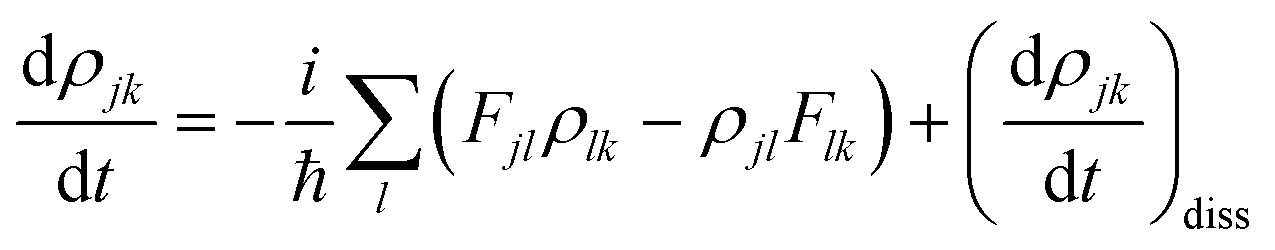
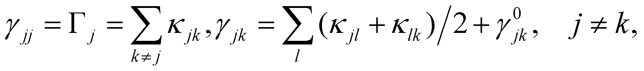
Fig. 1 shows a Si slab with a Si (111):H surface and large adsorbed clusters; the slab contains four layers each with an array of 6 × 10 Si atoms with surface bonds saturated by H atoms. Adsorbed Ag32, Ag33, Ag34 and Ag37 clusters were generated as truncated Ag55 clusters along different cluster planes compatible with the substrate Si(111) lattice. Structures were optimized with projector augmented wave (PAW) potentials and plane wave basis sets.49 DFT calculations have been performed using the Vienna ab initio simulation package (VASP).39,50 The structures were obtained from calculations using the generalized gradient approximation (GGA) of Perdew–Burke–Ernzerhof (PBE) with an exchange–correlation functional. The convergence criteria for the relaxed structures have been set to 10 meV Å−1 for the residual forces. Due to the larger size of the super cell, the Brillouin zone is sampled at the Gamma point only. The slabs were generated by periodically translating a supercell as shown in panels (a) for Ag32Si240H52, (b) for Ag33Si240H52, (c) for Ag34Si240H52, and (d) for Ag37Si240H52. The adsorbed structures are semi-spherical, with the Ag atoms in AgnSi240H52 forming a dome shape.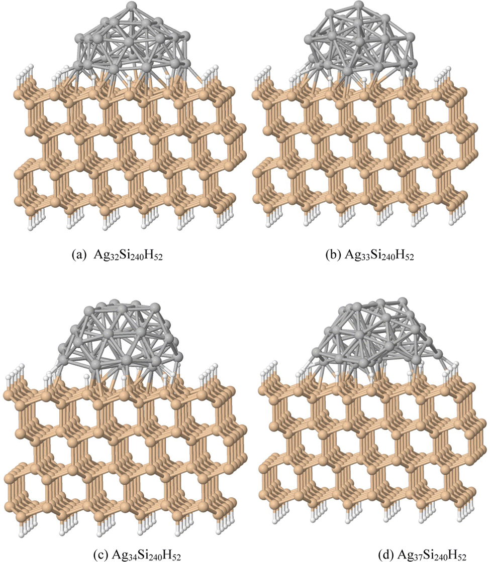 | ||
| Fig. 1 (a) The Ag32Si240H52 supercell structure generates a nanostructured surface by periodically translating the supercell as shown, with the Si surface perpendicular to a z-axis, along x- and y-directions of the surface plane, and was optimized using the PBE functional. (b) Ag33Si240H52, (c) Ag34Si240H52 and (d) Ag37Si240H52 structures were similarly optimized. | ||
Since HSE06 optimizations are expensive, and its results for ground state structures are similar to the PBE ones, we have done the following calculations of optical properties with the HSE06 functional, using however, PBE optimized structures.
3 Ab Initio and density matrix treatments
The equation of motion (EOM) for the reduced density matrix (RDM) with KSOs as a basis set, in the Schrödinger picture, is27,28,46,51,52Here the matrix elements Fjl are obtained from an effective Hamiltonian describing active electrons in the physical system and includes their dipole coupling to an external electric light field oscillating with frequency ΩL. The last term is a dissipative rate due to the interaction of active electrons with electronic density fluctuations and lattice vibrations in the slab. The time dependence due to the applied field can be removed from the EOM making a transformation to a rotating frame, which introduces the new matrices
![[small rho, Greek, tilde]](https://www.rsc.org/images/entities/i_char_e0e4.gif) jk.46,51,53 The dissipative rate term can be approximated, in the limit of long times compared with relaxation times of the active electrons, as done in the Redfield treatment of relaxation,51 introducing state-to-state transition rates induced by interaction of active electrons with their medium.
jk.46,51,53 The dissipative rate term can be approximated, in the limit of long times compared with relaxation times of the active electrons, as done in the Redfield treatment of relaxation,51 introducing state-to-state transition rates induced by interaction of active electrons with their medium.
In the rotating wave approximation, the steady state values ssjj for the diagonal elements of the reduced density matrix including dissipation due to lattice vibrations are obtained setting the left hand side of the EOM equal to zero, or djk/dt = 0, and are given (with HO for highest occupied and LU for lowest unoccupied orbitals) by46

 from a state-to-state transition rate κjk = |Vjk|2J(ωjk)fBE(ωjk,T). Also, Vjk is a phonon-induced transition energy, J(ωjk) is a vibrational frequency density, and fBE(ωjk,T) is a thermal Bose–Einstein distribution of phonons. The Rabi frequency due to the coupling of the electronic transition dipole and external photon field is given by
 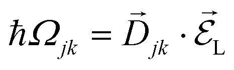 , and Δjk = ΩL − ωjk is the detuning frequency obtained from the band energies of initial and final orbitals. Here ΩL is the frequency of photons with energy ħΩL. The factor
 ![[D with combining right harpoon above (vector)]](https://www.rsc.org/images/entities/i_char_0044_20d1.gif) jk is the transition dipole moment for the interband transition from orbital j in the VB to k in the CB, projected on the direction of the electric field vector
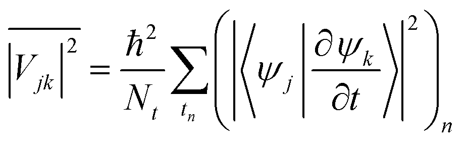
jk is the transition dipole moment for the interband transition from orbital j in the VB to k in the CB, projected on the direction of the electric field vector  . In general, the electric field is at an angle with the semiconductor surface, and the transition dipole has parallel and perpendicular components. Here we consider the excitations induced by a distribution of light angles, with jk interpreted as an average perpendicular to the surface. Electron-phonon coupling rates can be obtained from ab initio MD and state-to-state nonadiabatic energy couplings averaged over Nt trajectories for the crystal ions, giving
However in the present treatment the depopulation and decoherence rates are simply parametrized from our knowledge of theoretical and experimental values. The electronic density of states (EDOS) is obtained from
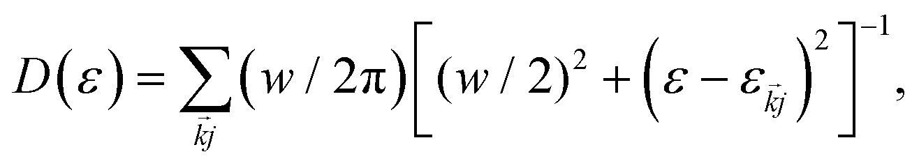 with the width parameter w = 20 meV.
4 Results for light absorbance and absorption flux
4.1 Band gaps and adsorbate levels
The KS orbital energies at the band gap region are listed in Table 1 from PBE and HSE06 calculations. In the case of open shell Ag cluster adsorbates such as Ag33Si240H52 and Ag37Si240H52 the valence band maximum (HOMO) is singly occupied. Results are also shown with the addition of long-range van der Waals dispersion energies as PBE + D3(BJ), which gives some improvements compared to HSE06 but too small band gaps. It is clear from Table 1 that addition of silver clusters drastically reduces the band gap of the nanostructured Si slabs from 1.61 eV to about 0.50 eV, according to HSE06 calculations.| Method | Energy levels (eV) | ||||
|---|---|---|---|---|---|
| HOMO(2) | HOMO(1) | LUMO | E LUMO–EHOMO(2) | E LUMO–EHOMO(1) | |
| Ag55 | |||||
| PBE | −2.6663 | −2.6344 | −2.5460 | 0.1203 | 0.0884 |
| HSE06 | −2.5870 | −2.4914 | −2.3348 | 0.2522 | 0.1566 |
| Si240H60 | |||||
| PBE | 1.0309 | 2.0180 | 0.9871 | ||
| HSE06 | 0.6552 | 2.2609 | 1.6057 | ||
| Ag33Si240H52 | |||||
| PBE | 0.6471 | 0.7552 | 0.9966 | 0.3495 | 0.2414 |
| PBE + D3(BJ) | 0.7292 | 0.7851 | 1.1131 | 0.3839 | 0.3280 |
| HSE06 | 0.5590 | 0.8026 | 1.1012 | 0.5422 | 0.2986 |
| Ag37Si240H52 | |||||
| PBE | 0.6377 | 0.8431 | 0.9728 | 0.3351 | 0.1297 |
| PBE + D3(BJ) | 0.7818 | 0.9759 | 1.1072 | 0.3254 | 0.1313 |
| HSE06 | 0.5468 | 0.8488 | 1.0602 | 0.5134 | 0.2114 |
| Ag32Si240H60 | |||||
| PBE | 0.7292 | 1.0447 | 0.3155 | ||
| HSE06 | 0.6978 | 1.1892 | 0.4914 | ||
| Ag34Si240H60 | |||||
| PBE | 0.6266 | 0.9825 | 0.3559 | ||
| HSE06 | 0.5718 | 1.1195 | 0.5477 | ||
The atomic structures of the adsorbates were optimized by energy minimization using PBE + D3(BJ). This also provided information on electronic charge transfers between the substrate and adsorbates. The total charge on Agn clusters in Ag32/Si and Ag34/Si structures are positive, +0.133 e and +0.118 e respectively, while the total cluster charge in Ag33/Si and Ag37/Si structures are negative, −0.039 e and −0.116 e respectively. However, since these calculations are done with plane wave basis sets (not localized basis sets), the charges on atoms are only approximate.
Energy band gaps obtained from ELUMO–EHOMO are physically accurate from HSE06 as compared with known experimental values for pure bulk Si, of 1.17 eV,54 but too small from PBE calculations. There are no experimental values for the Si slab we have modelled here, but our previous calculations23 for varying slab thickness have shown the correct trend of HSE06 energy gaps as thickness grows toward the experimental bulk Si energy gap value.
4.2 Electronic density of states (EDOS)
Fig. 2 below shows comparisons of EDOSs D(ε), where ε = ħΩL is a photon energy, from HSE06 calculations. The curves are seen to have very similar shape for different AgnSi240H52 structures. Comparison of the total electronic density of states EDOS for Ag32 and Ag34, two structures with closed shells, with the EDOS for open-shell Ag33 shows how the unpaired electron in this cluster gives a new state in the energy band gap. Partial atomic and (EDOSs) versus orbital energies are also shown in Fig. 3 for the open-shell structure cluster in Ag33Si240H52, from the PBE and HSE06 functionals. The curves are seen to have very similar shape but the HSE results are stretched out from the energy origin chosen at the doubly occupied EHOMO(2). It clearly shows how HSE gives a larger band gap, and displays a large change in the location of states coming from the Ag atoms. Comparing its DOS with the one for Ag32Si240H52 in Fig. 2 shows where the additional Ag atom has added electronic states near the band gap region. A band-gap corrected PBE + BG procedure (not shown here), consisting of shifting energy levels of PBE above the valence band by the difference between HSE and PBE band gaps, would give results similar to HSE.23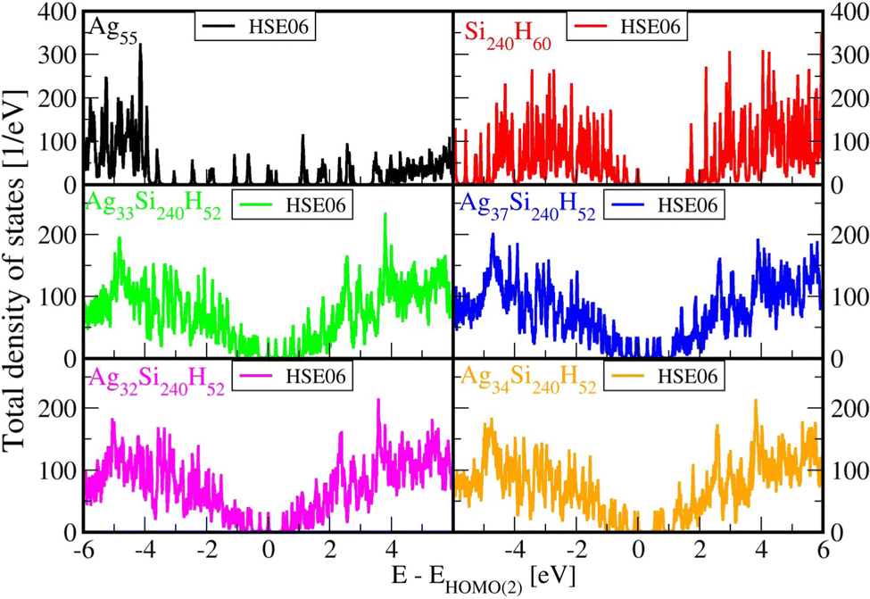 | ||
| Fig. 2 Comparisons of electronic density of states for the studied AgnSi240H52 structures using HSE06 functionals. The energy axes are shifted to start (zero in the x-axis) with the highest doubly occupied KS orbital, so that here ε = E(KS orbital) − EHOMO(2) for both open and closed shell systems. | ||
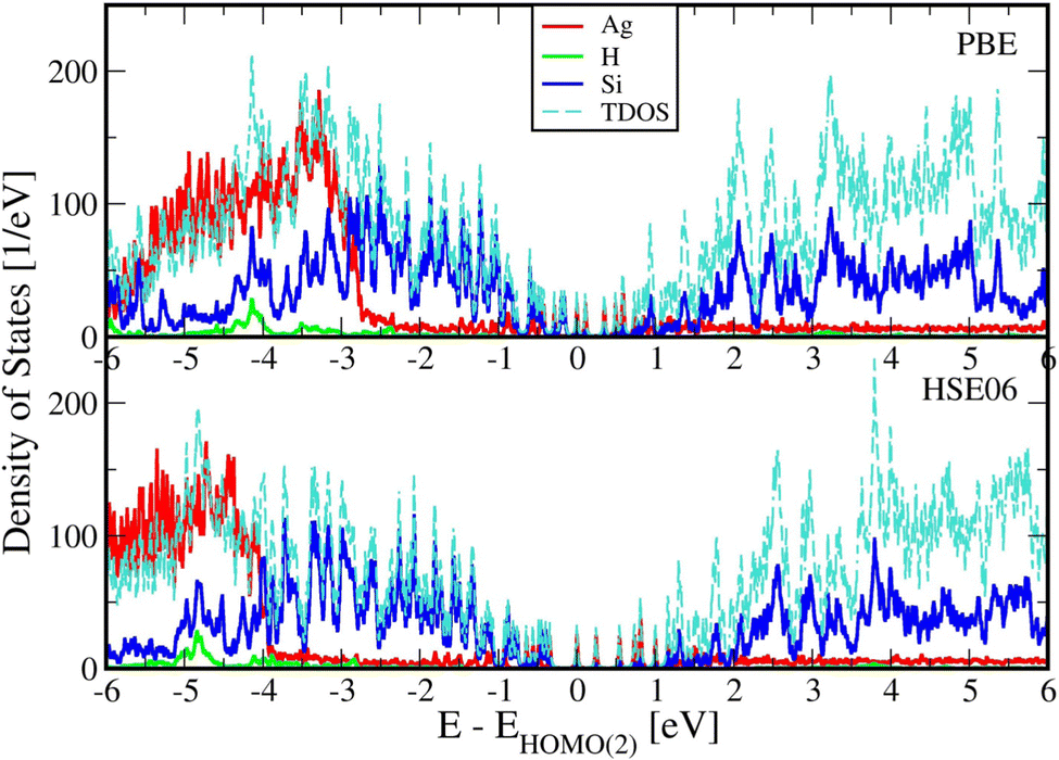 | ||
| Fig. 3 Partial and total electronic density of states (EDOSs) for Ag33Si240H52 from PBE and HSE06 functionals. Total and Projected Density of States (PDOS) plots for Ag33Si240H52 use a width of w = 20 meV. The energy axes are shifted to start (zero in the x-axis) with the highest doubly occupied KS orbital as discussed earlier. The Ag33 cluster adds new electronic levels in the band gap region. | ||
The rapidly oscillating lines in Fig. 2 and 3 around average values of the EDOSs result from calculations of individual energy levels of the structures, using a width of w = 20 meV for the levels in graphs. They have been shown here to illustrate how the EDOSs contain features of both small and large molecular (or cluster) systems. The oscillations would be smaller with larger assumed level widths. Also, the results here have been shown for the Gamma point of the Brillouin zone of the reciprocal space for the Si(111) crystal structure. The curves would be somewhat smoother if averaged over a number of k-points of the Brillouin zone. However, our experience from extensive photoconductivity calculations for these slab systems is that energy bands are flat and k-point averages involve minor changes in the intensity of light absorption.55
Spin-polarized calculations (not included here) with separate electronic densities for up and down spins of open-shell adsorbates have been done with HSE06 for Ag33Si240H52. They show a difference in the band gaps calculated for up and down spins, but they are of the same magnitude as the band gap without spin polarization. Insofar the following results on light absorbance are obtained from sums over all states it is expected that the total values of intensities will be similar for non-polarized and polarized DOSs. The same arguments apply for the open-shell cluster in Ag37Si240H52.
Calculations using the HSE06 hybrid functional are more demanding than those from PBE, which does not require generation of electron exchange at the Hartree–Fock level of modelling. In extensive calculations for many cluster structures it is possible to bypass the hybridization using modified PBE functionals. A band gap correction procedure has previously been introduced, called PBE + BG,23 which extracts an energy shift for the valence band by comparison of HSE06 and PBE band gap results, and has been found to provide acceptable EDOSs and light absorbance shapes while being much less demanding of computing times, but is not further considered here. Another alternative is the DFT+U procedure which has been used also for Ag5/TiO2.35
5 Light absorbance and absorption flux
Photoinduced electronic populations Δnss(ε,ħΩL) follow from the energy levels and their populations as given by the diagonal elements of the RDM, so thatThe absorbed light flux Fabs(ΩL) is calculated from linear response theory using ab initio electronic structure calculations for an incident flux Finc(ħΩL).28 The excitation energies and transition dipole moments have been obtained from KSOs generated with both PBE and HSE06 functionals in VASP calculations, and used in
where
 is a normalized state-to-state oscillator strength per active electron (with a number
  of active electrons) obtained as
with ħΩjk = DjkL and ħγ = 0.01 eV.
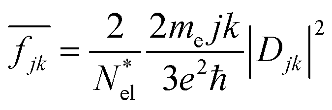
Results are shown in Fig. 4 obtained for an incident flux versus photon energy corresponding to sunlight: black body radiation rate at T = 5800 K. This peaks around 1.9 eV and dampens the flux curves at large photon energies. The large differences in band gaps values between PBE and HSE06 results have a very large effect on the absorption fluxes and their relative values without and with Ag cluster adsorbates. Here we show only the HSE06 results.
 | ||
| Fig. 4 Light absorbance vs. photon energy for the present Agn/Si(111) structures, pure Si surface and Ag55 using the HSE06 functional. In the upper panel the Ag55 values are shown, and in the lower panel Agn/Si(111) structures and pure Si surface absorption values are shown. | ||
The large difference between the absorption flux by Ag55 and by the adsorbed cluster can be attributed to the extensive redistribution of electronic charges at the interface of the Ag clusters with the Si(111) slab surface. Hybridization of Ag and Si orbitals at the interface lead to local charge transfer and formation of ground state and excited state molecular orbitals for the whole system, and to quite different transition dipoles.
6 Evidence for localized plasmons in the near IR to near UV spectral regions and a mesoscopic model for plasmons
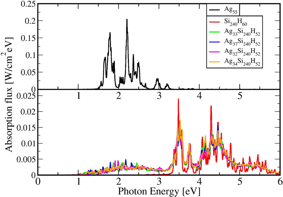
Table 2 below shows the absolute and relative absorption values obtained from KSOs generated with the HSE06 functionals in DFT calculations, in the photon energy interval [0.5,3.0] eV. Fig. 5 shows the difference in absorption flux values of Agn/Si(111) structures compared to values for the pure Si(111) slab. Comparing the absorption profiles for the pure Si slab and the slab with adsorbates, we find that a large light absorption increase has occurred between 2 and 3 eVs.| System | Absolute integrated absorption in the [0.5,3.0] eV range from HSE06 | Relative integrated absorption in the [0.5,3.0] eV range from HSE06 |
|---|---|---|
| Si240H60 | 0.00012 | 1.00 |
| Ag33Si240H52 | 0.00311 | 26.58 |
| Ag37Si240H52 | 0.00333 | 28.50 |
| Ag32Si240H52 | 0.00313 | 26.72 |
| Ag34Si240H52 | 0.00332 | 28.3 |
 | ||
| Fig. 5 Difference in absorption spectra for pure Si240H60, Ag33Si240H52, Ag37Si240H52, Ag32Si240H52, and Ag34Si240H52 in the 0.5 to 3.0 eV photon energy range using the HSE06 functional. | ||
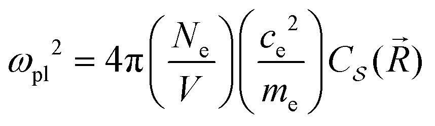
It is possible to provide a qualitative understanding of the location and shapes of the calculated light absorption curves, with simple arguments relating to the frequencies of plasmon absorption as they relate to densities of finite metallic compounds. The plasmon frequency ωpl for the solid Ag metal has an energy ħωpl = 8.9 ± 0.2 eV, and it can be related to the electronic density per unit volume (in SI units) by ωpl2 = nee2/(ε0me). However, in our clusters, we are concerned with spherical and semi-spherical metal structures, and we know that a sphere instead obeys the relation ωpl2 = nee2/(ε03me) for its electron gas,56 which gives a value of ħω(sp)pl = 5.14 eV for the plasmon frequency of a Ag sphere of the same electron density. In addition, we have two other features affecting the plasmon frequency: (a) in our adsorbates half a sphere is submerged into the Si slab, with a much smaller electron density, which gives an average density about ½ smaller and approximately ħω(ssp)pl = 3.65 eV; (b) it is known that surface plasmons satisfy (ω(surf)pl)2 = ωpl2/2 and some of the outer layer of our clusters must account for this decrease. Therefore, we can qualitatively expect that plasmon absorption peaks for our clusters will appear below about 3 eV, as it is found in our calculations. The largest increases in our calculated absorbance in Fig. 5, due to the presence of the clusters, occur around 2.3 eV, as we expected for our localized plasmons.
A useful and straightforward treatment of large adsorbed clusters can be based on the definition of mesoscopic properties of a sufficiently large collection of Nat atoms in a nanoparticle  containing the adsorbed cluster plus a localized region of the slab bonding to the cluster, so that Nat = Ncl + Nbd. Some related treatments can be found in the recent literature.43,57 That localized subsystem in the nanostructured surface can be taken to be spherical-like, with a half-sphere enclosing the cluster and the other half containing the slab bonding atoms. The optical properties of this system can be obtained from the dynamics of mesoscopic properties defined at points
 ![[R with combining right harpoon above (vector)]](https://www.rsc.org/images/entities/i_char_0052_20d1.gif) of the localized system. For an applied oscillating electric field
of the localized system. For an applied oscillating electric field  of frequency Ω, an element of volume located at with its mass density per unit volume μ() and its charge density per unit volume c() is subject to an external electric force
  , which generates charge density oscillations, or plasmons, in the x-direction parallel to the slab surface.
A local electronic polarizability operator (the electronic dipole per unit volume) is given by
![[r with combining right harpoon above (vector)]](https://www.rsc.org/images/entities/i_char_0072_20d1.gif) . This operator has a statistical average given in terms of the steady-state RDOp
. This operator has a statistical average given in terms of the steady-state RDOp ![[small rho, Greek, circumflex]](https://www.rsc.org/images/entities/i_char_e0b7.gif) (ss)(Ω) of
(ss)(Ω) of  by
by  and in particular for the x-direction by
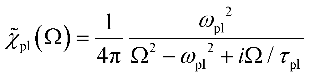
which provides the susceptibility

 and the dielectric function
  (in the cgs Gaussian units).
To simplify the following treatment, omitting and for the x-direction, the total dielectric function is ε(Ω) = 1 + 4π[χel(Ω) + χion(Ω) + χmed(Ω)], with the two last terms from the ionic lattice and medium atoms taken in what follows as constant in the range of visible and near IR frequencies of interest here. This gives ε(Ω)1/2 = η(Ω) + iκ(Ω), with the real part refraction index η and imaginary part as the extinction coefficient κ, and a light absorbance α = 2Ωκ(Ω)/(cη),58 where c is the speed of light here and the magnetic susceptibility constant has been set to μ = 1. Again, η can be taken to be a constant.
In the mesoscopic treatment, the electronic polarizability created by plasmon oscillations of amplitude Xpl(t) (for the given field polarization) is 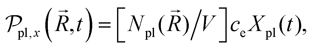 with a mass μpl() of plasmons driven by the applied electric field. These oscillations are further subject to a Lorentz restoring force coming from the distribution of ion and electron charges in the system, written here as –k()Xpl, and to a dissipative Drude friction
 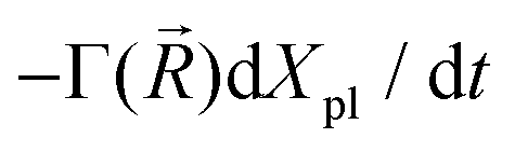 . Its equation of motion is, with
  ,
,
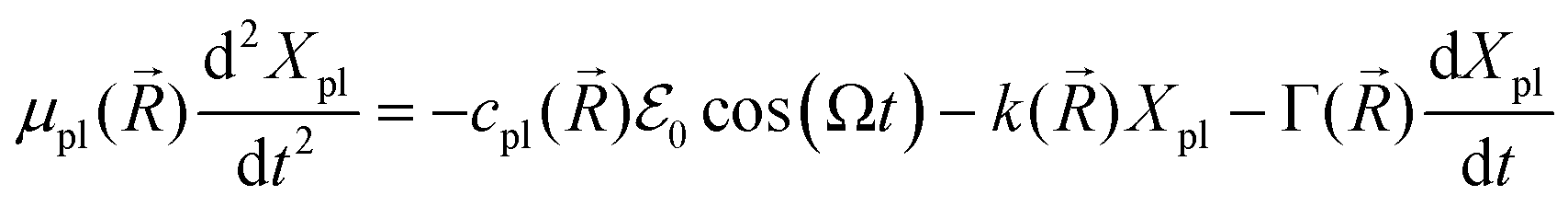
where
 depends on the structure of the nanoparticle, and equals unity for the homogeneous electron gas. Furthermore, the friction rate coefficient can be re-expressed in terms of a plasmon relaxation time τpl as Γ = μpl/τpl.
It is convenient to work with complex quantities and take their real part at the end, with ![[X with combining tilde]](https://www.rsc.org/images/entities/i_char_0058_0303.gif) (t) = 0exp(iΩt) and X(t) = Re[(t)], giving for plasmons the solution
(t) = 0exp(iΩt) and X(t) = Re[(t)], giving for plasmons the solution 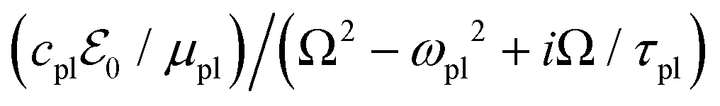 . This provides the complex polarization per unit volume
 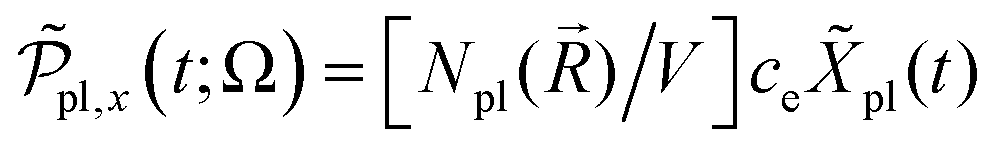 and the amplitude
 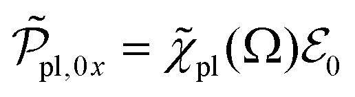 with the susceptibility function
For |4πχpl| ≪ 1 and approximating the square root in 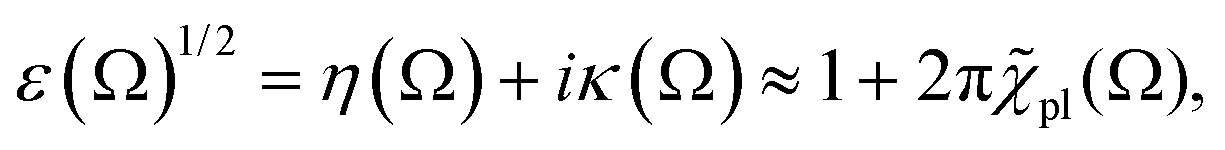 this gives
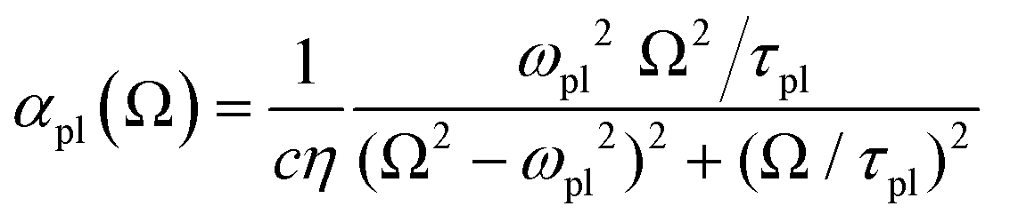
 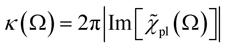 and the plasmon light absorbance per unit length
For a nanoparticle  of volume
  with
with  active electrons per unit volume, it is convenient to introduce a normalized oscillator strength
 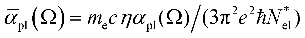 of dimensions volume over energy.29 This line shape contains the two parameters ωpl2 and τpl, giving the frequency and lifetime of the plasmon. The two values can be extracted from our calculations of light absorption of photons with energy ħΩ, from which we obtain the plasmon absorption flux Fpl(ħΩ) =
 ![[small alpha, Greek, macron]](https://www.rsc.org/images/entities/i_char_e0c2.gif) pl(Ω)frad(Ω,T)ħΩ where frad(Ω,T) is the black body radiation distribution per unit energy and unit volume at T = 5800 K.29
pl(Ω)frad(Ω,T)ħΩ where frad(Ω,T) is the black body radiation distribution per unit energy and unit volume at T = 5800 K.29
As an example, the difference in pl(Ω) between the values for the adsorbate Ag32/Si and pure Si has been calculated with two separate HSE06 calculations and their subtraction, and the result has been fit with the function pl(Ω) for ħΩ = 0.5 to 3.0 eV, to extract the adsorbate plasmon frequency and lifetime of ωpl = 3.9 × 10¹⁵ s−1 (ħωpl = 2.56 eV) and τpl = 0.5 × 10⁻¹⁵ s = 0.5 fs. These can be compared with the values for the pure Ag solid at room temperature,59 with plasmon frequency ωpl[Ag(s)] = 13.64 × 10¹⁵ s−1 = 9.0 eV ħ−1, electron density ne = Ne/V = 5.9 × 1022 cm−3, and τpl[Ag(s)] = 3.8 × 10⁻¹⁴ s. As expected, the plasmon frequency for the adsorbate cluster is smaller due to its localized nature, and the smaller adsorbate plasmon lifetime is likely due to the presence of a large number of vibronic energy levels at the surface, available for the decay of the adsorbate cluster electronic excitation.
7 Conclusion
This work extends our previous model results, to include here light absorption of larger Ag clusters adsorbed on Si slabs. Our treatment gives results for an atomistic treatment of both adsorbed clusters and their semiconductor substrate, combining an accurate density functional treatment of electronic structure and a reduced density matrix formulation of the dissipative dynamics for the photoexcited clusters.Ab initio results from atomic structures show that large Ag cluster adsorbates increase light absorption by large percentages. Calculations with correct band gaps, such as given by the hybrid functional HSE06, are essential. Our results show that intensities of light absorbance have features with high peaks similar to absorption by small molecules, but also broad features that can be related to collective electronic excitations, or localized plasmons, for our clusters. The energy band gap for Si(111) is well known, but there are no experimental measurements of band gaps for the nanostructured Si slabs of the present work. Our calculations and explanations of plasmonic behavior in our systems have identified the range of photon energies relevant to light absorption by plasmon excitation, and have provided insight on the physical phenomena relating to localized plasmons in realistic systems.
A mesoscopic model has been described that provides insight on the location of peaks in the light absorbance and relates them to plasmon-like excitations for our localized metal structures. Our mesoscopic treatment introduces novel equations of motion of electronic densities driven by light, and their solutions for adsorbed clusters, to describe the shapes of light absorption lines. Fitting calculated plasmon shapes it has been possible to estimate the magnitudes of the adsorbate plasmon frequency and lifetime in a special case.
The present large plasmon-like excitation increments in absorbance of light occur in regions of the spectra around 2 eV, and extend over a range which overlaps with the solar spectra, so that the present results may be significant for applications of the present nanostructured surfaces to devices for solar photoconductivity and photocatalysis.
The choice of Ag is not exclusive, and calculations could have been done for Au or Cu. However, when it comes to relevance to photovoltaics, there is some evidence that Cu atoms on Si would diffuse, and Au would be more expensive in the preparation of materials for photovoltaics. This has led us and other researchers to focus on Ag clusters when the substrate is a Si surface.
Conflicts of interest
There are no conflicts to declare.Acknowledgements
This work has been partly supported by the National Science Foundation grant NSF CHE 1445825 to DAM. Computing support was partly provided by the High Performance Computing facility of the University of Florida. TV thanks the Anupam supercomputing facility at Bhabha Atomic Research Centre, Trombay, India for computing support. D. K. acknowledges support of grants NSF CHE-1944921 for development of methods for excited state dynamics and NSF CHE-2004197 for exploration of interfacial charge transfer.References
- M. L. Cohen and W. D. Knight, The physics of metal clusters, Phys. Today, 1990, 1990, 42 CrossRef.
- V. Bonacic-Koutecky, P. Fantucci and J. Koutecky, Quantum chemistry of small clusters of elements of groups Ia, Ib, and IIa: Fundamental concepts, predictions, and interpretation of experiments, Chem. Rev., 1991, 91, 1035 CrossRef.
- W. A. deHeer, The physics of simple metal clusters: Experimental aspcets and simple models, Rev. Modern Phys., 1993, 65, 611 CrossRef.
- U. Kreibig and M. Vollmer, Optical properties of metal clusters, Springer-Verlag, Berlin, 1995 Search PubMed.
- S. Link and M. A. ElSayed, Optical properties and ultrafast dynamics of metallic nanocrystals, Ann. Rev. Phys. Chem., 2003, 54, 331 CrossRef PubMed.
- A. P. Alivisatos, Semiconductor clusters, nanocrystals, and quantum dots, Science, 1996, 271, 933 CrossRef.
- A. J. Nozik, Spectroscopy and hot electron relaxation dynamics in semiconductor quantum wells and quantum dots, Ann. Rev. Phys. Chem., 2001, 52, 193 CrossRef.
- P. V. Kamat, Quantum dot solar cells. Semiconductor nanocrystals as light harvesters, J. Phys. Chem. C, 2008, 112, 18737 CrossRef.
- S. Pillai, K. R. Catchpole, T. Trupke and M. A. Green, Surface plasmon enhanced silicon solar cells, J. Appl. Phys., 2007, 101, 093105 CrossRef.
- T. W. Odom and G. C. Schatz, Plasmonics (Special Issue), Chem. Rev., 2011, 111, 3667 CrossRef PubMed.
- N. J. Halas, S. Lal, W. S. Chang, S. Link and P. Nordlander, Plasmons in Strongly Coupled Metallic Nanostructures, Chem. Rev., 2011, 111, 3913 CrossRef PubMed.
- C. Clavero, Plasmon-induced hot-electron generation at nanoparticle/metal-oxide interfaces for photovoltaic and photocatalytic devices, Nat. Photonics, 2014, 8, 95 CrossRef.
- D. A. Micha, Density matrix treatment of optical properties in photovoltaic materials: Photoconductivity at a semiconductor surface, Photoinduced Processes at Surfaces and in Nanomaterials, Chap. 7. American Chemical Society, New York, 2015. p. 151 Search PubMed.
- A. Fernando, K. L. Dimuthu, M. Weerawardeme, M. D. Karimova and C. M. Aikens, Quantum mechanical studies of large metal, metal oxide, and metal chalcogenide nanoparticles and clusters, Chem. Rev., 2015, 115, 6112 CrossRef PubMed.
- Y. H. Jang, Y. J. Jang, S. Kim, L. N. Quan, K. Chung and D. H. Kim, Plasmonic Solar Cells: From Rational Design to Mechanism Overview, Chem. Rev., 2016, 116, 14982–15034 CrossRef PubMed.
- A. Campos, N. Troc, E. Cottancin, M. Pellarin, H. C. Weisker and J. Lerme, et al., Plasmonic quantum size effects in silver nanoparticles are dominated by interfaces and local environments, Nat. Phys., 2019, 15, 275 Search PubMed.
- V. Bonacic-Koutecky and R. Antoine, Enhanced two-photon absorption of ligated silver and gold nanoclusters: Theoretical and experimental assesments, Nanoscale, 2019, 11, 12436 RSC.
- S. Tan, A. Argondizzo, J. Ren, L. Liu, J. Zhao and H. Petek, Plasmonic coupling at a metal/semiconductor interface, Nat. Photonics, 2017, 11, 806–812 CrossRef.
- K. Ueno, T. Oshikiri, Q. Sun, X. Shi and H. Misawa, Solid-State Plasmonic Solar Cells, Chem. Rev., 2018, 118, 2955–2993 CrossRef.
- J. M. J. Martirez, J. L. Bao and E. A. Carter, First-Principles Insights into Plasmon-Induced Catalysis, Annu. Rev. Phys. Chem., 2021, 72, 99 CrossRef PubMed.
- M. P. de Lara-Castells, First-principles modelling of the new generation of subnanometric metals: clusters: recent case studies, J. Colloid Interface Sci., 2022, 612, 737 CrossRef PubMed.
- D. S. Kilin and D. A. Micha, Modeling the photovoltage of doped Si surfaces, J. Phys. Chem. C, 2011, 115, 770 CrossRef.
- T. Vazhappilly and D. A. Micha, Computational modeling of the dielectric function of a silicon slab with varying thickness, J. Phys. Chem. C, 2014, 118, 4429 CrossRef.
- R. Hembree, T. Vazhappilly and D. A. Micha, Quantum confinement effects on electronic photomobilities at nanostructured semiconductor surfaces: Si(111) without and with adsorbed Ag clusters, J. Chem. Phys., 2017, 147, 224703 CrossRef PubMed.
- T. Vazhappilly, M. P. de Lara-Castells and D. A. Micha, Model studies of the structure and optical properties of the TiO2(110) surface with an adsorbed Ag atom, Mol. Phys., 2019, 117, 2267–2274 CrossRef.
- M. P. de Lara-Castells, C. Cabrillo, D. A. Micha, A. O. Mitrushchenkov and T. Vazhappilly, Ab initio design of light absorption through silver atomic cluster decoration of TiO2, Phys. Chem. Chem. Phys., 2018, 20, 19110–19119 RSC.
- D. A. Micha, Density Matrix Theory and Computational Aspects of Quantum Dynamics in an Active Medium, Int. J. Quantum Chem., 2000, 80, 394–405 CrossRef.
- D. A. Micha, Generalized response theory for a photoexcited many-atom system, Advances in Quantum Chemistry, Elsevier-Wiley, New York, 2015. p. 195 Search PubMed.
- T. Vazhappilly, D. S. Kilin and D. A. Micha, Photoabsorbance and Photovoltage of Crystalline and Amorphous Silicon Slabs with Silver Adsorbates, J. Phys. Chem. C, 2012, 116, 25525 CrossRef.
- T. W. Lajoie, J. J. Ramirez, D. S. Kilin and D. A. Micha, Optical properties of amorphous and crystalline silicon surfaces functionalized with Agn adsorbates, Int. J. Quantum Chem., 2010, 110, 3005–3014 CrossRef.
- X. J. Xi, J. S. Yang, J. Y. Wang, X. Y. Dong and S. Q. Zang, New Stable Isomorphous Ag34 and Ag33 Nanoclusters with an Open Shell Electronic Structure, Nanoscale, 2018, 10, 21013–21018 RSC.
- Y. Han, D. A. Micha and D. S. Kilin, Ab initio study of the photocurrent at the Au/Si metal-semiconductor nanointerface, Mol. Phys., 2015, 113, 327–335 CrossRef.
- S. L. Brown, E. K. Hobbie, S. Tretiak and D. S. Kilin, First-principles study of fluoresecence in silver nanostructures, J. Phys. Chem. C, 2017, 121, 23875 CrossRef.
- M. P. de Lara-Castells, A. W. Hauser, J. M. Ramallo-Lopez, D. Buceta, L. J. Giovanetti and M. A. Lopez-Quintela, et al., Increasing the optical response of TiO2 and extending it into the visible region through surface activation with highly stable Cu5 clusters, J. Mater. Chem. A, 2019, 7, 7489–7500 RSC.
- P. Lopez-Caballero, J. M. Ramallo-Lopez, L. J. Giovanetti, D. Buceta, S. Miret-Artes and A. Lopez-Quintela, et al., Exploring the properties of Ag5–TiO2 interfaces: stable surface polaron formation, UV-Vis opticalresponse, and CO2 photoactivation, J. Mater. Chem. A, 2020, 8, 6842–6853 RSC.
- A. Vijay, G. Greg Mills and H. Metiu, Adsorption of gold on stoichiometric and reduced rutile TiO2(110) surfaces, J. Chem. Phys., 2003, 118, 6536 CrossRef.
- S. Linic, P. Christopher and D. B. Ingram, Plasmonic-Metal Nanostructures for Efficient Conversion of Solar to Chemical Energy, Nat. Mater., 2011, 10, 911–921 CrossRef PubMed.
- L. Liu and A. Corma, Metal Catalysts for Heterogeneous Catalysis: From Single Atoms to Nanoclusters and Nanoparticles, Chem. Rev., 2018, 118, 4981–5079 CrossRef PubMed.
- G. Kresse and J. Furthmuller, Efficient iterative schemes for ab initio total energy calculations using a plane wave basis set, Phys. Rev. B: Condens. Matter Mater. Phys., 1996, 54, 11169–11186 CrossRef PubMed.
- J. P. Perdew, K. Burke and M. Ernzenhof, Generalized gradient approximation made simple, Phys. Rev. Lett., 1996, 77, 3865 CrossRef PubMed.
- J. Heyd and G. E. Scuseria, Efficient hybrid density functional calculations in solids: assessment of the Heyd–Scuseria–Ernzerhof screened Coulomb hybrid functional, J. Chem. Phys., 2004, 121, 1187 CrossRef CAS.
- N. W. Ashcroft and N. D. Mermin, Solid State Physics, Thomson, England, London, 1976 Search PubMed.
- V. I. Zakomirnyi, Z. Rinkevicius, G. V. Baryshnikov, L. K. Sørensen and H. Agren, Extended Discrete Interaction Model: Plasmonic Excitations of Silver Nanoparticles, J. Phys. Chem. C, 2019, 123, 28867 CrossRef.
- D. A. Micha and T. Vazhappilly, An extended Drude–Lorentz model for adsorbates, UF-QTP Notes, Gainesville, Florida, USA, 2017, tbp Search PubMed.
- P. Nozieres and D. Pines, The Theory of Quantum Liquids, Perseus, Cambridge MA, 1999 Search PubMed.
- D. S. Kilin and D. A. Micha, Surface photovoltage at nanostructures on Si surfaces: Ab initio results, J. Phys. Chem. C, 2009, 113, 3530 CrossRef.
- S. M. Morton, D. W. Silverstein and L. Jensen, Theoretical Studies of Plasmonics Using Electronic Structure Methods, Chem. Rev., 2011, 111, 3962–3994 CrossRef PubMed.
- C. Yu, R. Schira, H. Brune, B. von Issendorff, F. Rabilloud and W. Harbich, Optical Properties of Size Selected Neutral Ag Clusters: Electronic Shell Structures and the Surface Plasmon Resonance, Nanoscale, 2018, 10, 20821–20827 RSC.
- R. M. Martin, Electronic Structure: Basic Theory and Practical Methods, Cambridge University Press, Cambridge, England, 2004 Search PubMed.
- J. Hafner, Ab Initio simulation of materials using VASP: density functional theory and beyond, J. Comput. Chem., 2008, 29, 2044–2078 CrossRef PubMed.
- V. May and O. Kuhn, Charge and Energy Transfer Dynamics in Molecular Systems, Wiley-VCH, Berlin, 2000 Search PubMed.
- D. A. Micha, Density matrix treatment of non-adiabatic photoinduced electron transfer at a semiconductor surface, J. Chem. Phys., 2012, 137, 22A521 CrossRef PubMed.
- R. Hembree II and D. A. Micha, Photoinduced Electron Transfer at a Si(111) Nanostructured Surface: Effect of Varying Light Wavelength, Temperature, and Structural Parameters, J. Chem. Phys., 2013, 138, 184708 CrossRef PubMed.
- O. Madelung, Semiconductor-Basic Data, Springer, New York, 1996 Search PubMed.
- T. Vazhappilly, R. Hembree and D. A. Micha, Photoconductivities from band states and a dissipative electron dynamics: Si(111) without and with adsorbed Ag clusters, J. Chem. Phys., 2016, 144, 024107 CrossRef PubMed.
- C. Kittel, Introduction to Solid State Physics, 8th edn, Wiley, Hoboken, NJ, 2005 Search PubMed.
- A. Agrawal, S. H. Cho, O. Zandi, S. Ghosh, R. W. Johns and D. J. Milliron, Localized Surface Plasmon Resonance in Semiconductor Nanocrystals, Chem. Rev., 2018, 118, 3121–3207 CrossRef CAS.
- D. A. McQuarrie, Statistical Mechanics, Harper & Row Publ., New York, 1973 Search PubMed.
- D. B. Tanner, Optical Effects in Solids, Cambridge University Press, Cambridge, England, 2019 Search PubMed.
| This journal is © the Owner Societies 2023 |