
Two-dimensional Cs3Sb2I9/C2N van der Waals type-II heterostructure: a promising photocatalyst for high efficiency water splitting†
Hui
Wang
,
Baozeng
Zhou
 * and
Wei
Li
*
* and
Wei
Li
*
Tianjin Key Laboratory of Film Electronic & Communicate Devices, School of Integrated Circuit Science and Engineering, Tianjin University of Technology, Tianjin 300384, China. E-mail: baozeng@tju.edu.cn; cliwei618@126.com
First published on 23rd November 2022
Abstract
The development of high-efficiency photocatalysts for photocatalytic hydrolysis using solar energy and water resources is of great significance for alleviating the current energy shortage. Finding rational photocatalysts remains a major challenge and great efforts have already been made. Here we propose a novel two-dimensional perovskite-based vdW heterostructure (Cs3Sb2I9/C2N) and systematically investigate its stability, electronic and optical properties and the effects of applied biaxial strain based on the first-principles approach to investigate its ability as a photocatalyst for water splitting. In order to ensure the significance of the calculation results in guiding experiments, a hybrid functional was used for all the calculations on the electronic structure. The results show that the Cs3Sb2I9/C2N heterostructure has satisfactory dynamic and thermal stability, and exhibits the characteristics of type-II band alignment in the equilibrium configuration. Charge density difference, Bader charge analysis and work function further prove that the photogenerated electrons flow from Cs3Sb2I9 to the C2N monolayer by the influence of the interface dipole, which promotes the separation and transfer of photogenerated charge carriers and inhibits the recombination of the photogenerated charge carriers. Furthermore, the Cs3Sb2I9/C2N heterostructure has a suitable redox potential for photocatalytic water splitting and exhibits enhanced light absorption in the visible light region. In addition, the electronic and optical properties of the Cs3Sb2I9/C2N heterostructure can be tuned by strain, and the Cs3Sb2I9/C2N heterostructure always possesses photocatalytic ability after applying −2% to 6% biaxial strain. These results suggest that the Cs3Sb2I9/C2N heterostructure will be a promising candidate for water splitting photocatalysts.
Introduction
Considering the increasing shortage of resources and the deterioration of the ecological environment in recent years, it has become a global sustainable development trend to urgently seek alternative energy sources that are environmentally friendly, cost-effective and renewable.1–3 Photocatalytic water splitting using solar energy to drive the sustainable production of hydrogen and oxygen has been recognized as an effective and promising strategy.4,5 Since the first report by Fujishima and Honda in 1972 to realize the overall photocatalytic water splitting of titanium dioxide (TiO2) electrodes,6 various photocatalysts have been extensively studied, such as metal oxides, nitrides, sulfides and other novel bulk semiconductor materials.7–14 An ideal photocatalyst for water splitting not only needs to possess suitable band-gap and band edge positions, strong visible light absorption and photochemical stability, but effective photogenerated carrier separation and high mobility are also key influencing factors.15 Therefore, a lot of research is still needed in this field in order to explore efficient photocatalytic water splitting materials.Due to the wide band-gap of traditional three-dimensional (3D) materials, the low utilization rate of visible light absorption, the low carrier mobility and long migration length can increase the recombination rate, resulting in the reduction of solar-to-hydrogen conversion efficiency, as a result, the photocatalytic ability is weakened.5,16,17 In contrast, two-dimensional (2D) materials are considered as excellent candidates for photocatalytic water splitting due to their tunable band-gap, large specific surface area, abundant active sites, and high carrier mobility.18,19 In the past few years, various 2D materials have been extensively explored experimentally and theoretically as photocatalysts for water splitting, such as monolayer transition metal dichalcogenides (TMDs),20,21 group III(IV) monohalides,19,22 graphitic carbonitrides (g-C3N4) and MXenes,23–25 many of which have shown great potential for photocatalytic water splitting. Unfortunately, the efficiency of 2D material photocatalysts is also limited due to the high recombination rate of photogenerated electron–hole pairs.2 Type II van der Waals (vdW) heterostructures with a staggered band structure can preserve the electronic and optical properties of both the monolayers, more importantly, the valence band maximum (VBM) and conduction band minimum (CBM) distributions in different layers, promoting the goal of achieving efficient separation of photogenerated electron–hole pairs, have been proposed as a better option.26–29 To date, a large number of novel type-II heterostructures have been developed with great potential for photocatalytic water splitting or photovoltaic applications.30–33
A novel two-dimensional layered semiconductor material C2N with a graphene-like structure was experimentally synthesized using a simple bottom-up wet chemical reaction method.34 C2N is a semiconductor with a direct band-gap of 2.47 eV, and has been widely studied in the field of optoelectronics and optical nanodevices due to its unique characteristics.35–37 For example, the on/off ratio of field effect transistor devices made of C2N materials is 107.34 Compared with other carbonitride materials, C2N has high water permeability, excellent chemical activity and better visible light absorption, and has been experimentally proved to be a potential photocatalyst.38 In 2000, Zemnukhova et al.39 reported that the halide perovskites, Cs3Sb2X9 (X = Cl, Br, and I), can be prepared from aqueous solutions of CsX and SbX3. Cs3Sb2X9 (X = Cl, Br, and I) perovskites are less toxic than Pb, and have excellent optoelectronic properties and good stability similar to those of lead halide perovskites, and have attracted intense research interest. Saparov et al.40 reported that the layered structure of the Cs3Sb2I9 perovskite could be prepared by a two-step deposition method, and density functional theory (DFT) calculations showed that the light absorption of Cs3Sb2I9 was comparable to that of CH3NH3PbI3. Yu-Liang Liu et al.41 demonstrated through theoretical studies that Cs3Sb2I9 is suitable for photocatalytic water splitting for hydrogen production or visible light-driven CO2 reduction. Despite the unprecedented rapid development of 3D perovskites in recent years, their stability under light and heat still hinders their widespread commercial applications.42,43 Accordingly, their corresponding 2D perovskites have received increasing research interest.44–46
In this paper, we constructed a Cs3Sb2I9/C2N heterostructure by vertically stacking Cs3Sb2I9 and C2N monolayers. The properties of the 2D layered Cs3Sb2I9/C2N vdW heterostructure were investigated using first-principles calculations. To explore the potential of this heterostructure, all our calculations employ hybrid density functional theory. The results show that the Cs3Sb2I9/C2N heterostructure has an inherent type-II band alignment, and the photogenerated electrons mainly accumulate in the C2N layer, while the Cs3Sb2I9 layer mainly accumulates holes, which promotes the effective separation of photogenerated carriers at the interface. Cs3Sb2I9/C2N has suitable redox band edges for photocatalytic water splitting. More obviously, the light absorption edge of the constructed Cs3Sb2I9/C2N heterostructure is significantly red-shifted compared to the monolayers and the light absorption is enhanced, which improves the photocatalytic performance. Finally, the effects of biaxial strain on the band-edge positions, electronic structure, and optical properties of the Cs3Sb2I9/C2N heterostructure are explored.
Computational details and models
The DFT based first-principles calculations are performed by using the Perdew–Burke–Ernzerhof generalized gradient approximation (PBE-GGA) for the exchange and correlation function as implemented in the Vienna ab initio simulation package (VASP).47,48 The projected augmented wave (PAW) method was used to describe the interactions between the valence and core electrons.49,50 The valence electron state of our vdW heterostructures and counterpart monolayer contains C(2s2p2), N(2s2p3), Cs(6s1), Sb(5s2p3), and I(5s2p5). The plane-wave basis set was used with an energy cut-off of 500eV throughout all the calculations. During the structural relaxation, the energy convergence criterion of the system is 10−6 eV, and the maximum forces on each atom are less than 0.01V Å−1. A sufficient vacuum space (∼25 Å) is added along the z-axis in order to prevent the interaction between adjacent periodic structures. The interlayer vdW interaction between Cs3Sb2I9 and C2N is corrected by using the DFT-D3 method of Grimme.51 Since the GGA-PBE functional usually leads to an underestimation of the band-gap, we used a screening parameter of 0.2 Å−1 and a 25% Heyd–Scuseria–Ernzerhof hybrid functional (HSE06) for all calculations to more accurately determine the properties.52 The Brillouin zone was set to be 9 × 9 × 1 and 5 × 5 × 1 Γ-centered k-mesh under PBE and HSE06 functionals, respectively. To ensure the structural stability of the Cs3Sb2I9/C2N heterostructure, the phonon dispersion spectrum is calculated using the finite displacement method on a 2 × 2 × 1 supercell with 128 atoms by using the PHONOPY package.53,54 In addition, the ab initio molecular dynamics (AIMD) simulations were performed at room temperature (300 K) with a time step of 1 fs for 5 ps to verify the thermodynamic stability of the heterostructure.Results and discussion
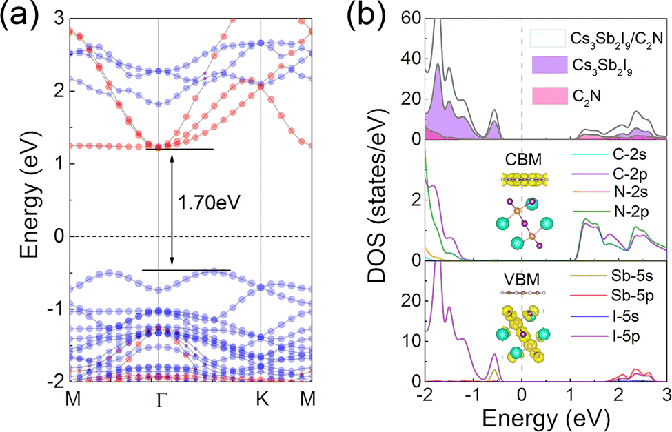
Before exploring the 2D vdW heterostructure, the structural and electronic properties of individual Cs3Sb2I9 and C2N layers were initially investigated. As shown in Fig. 1(a) and (b), the 2D monolayer Cs3Sb2I9 is a structure consisting of dioctahedral Sb2I9−3 dimer-like units with corner-sharing connectivity surrounded by cesium cations. The C2N monolayer structure is a planar honeycomb structure of C2 monolayers of benzene rings linked by nitrogen atoms. After full structural optimization, the obtained lattice parameters of the Cs3Sb2I9 and C2N monolayers are 8.58 Å and 8.33 Å, respectively, in agreement with previous experimental and theoretical reports,37,41 confirming the reliability and accuracy of our calculations. Fig. 1(c) and (d) show the band structures of the Cs3Sb2I9 and C2N monolayers calculated using the HSE06 method, one can observe the band-gaps of 2.36 eV and 2.47 eV for Cs3Sb2I9 and C2N monolayers, respectively. These values are all in good agreement with the previous experimental or theoretical results.26,37,41 Furthermore, the Cs3Sb2I9 monolayer shows an indirect band-gap, which is supported by the CBM being positioned at the high symmetric Γ point, while the VBM is present between Γ and K points. In contrast, both the CBM and VBM locate at the Γ point of the C2N monolayer, exhibiting the properties of direct band-gap semiconductors. The calculated total density of states (TDOS) and projected density of states (PDOS) of the Cs3Sb2I9 and C2N monolayers as plotted in Fig. 1(e) and (f). For the Cs3Sb2I9 monolayer, it is evident that the CBM is primarily occupied by the I-5p and Sb-5p states, while the VBM is mainly dominated from the I-5p states and a small contribution from the Sb-5s states. For the monolayer C2N, C-2p and N-2p states play the necessary role in the CBM and VBM with strong orbital hybridization. | ||
| Fig. 1 Top and front views of the optimized geometric atomic structures of (a) Cs3Sb2I9 and (b) C2N monolayers. (c) and (d) Schematics of the band structures of Cs3Sb2I9 and C2N monolayers calculated using the HSE06 functional. The Fermi level (black dashed line) is shifted to zero. (e) and (f) Calculated TDOS and PDOS for Cs3Sb2I9 and C2N monolayers based on HSE06. | ||
The Cs3Sb2I9/C2N vdW heterostructure studied in this work is composed of 1 × 1 Cs3Sb2I9 and 1 × 1 C2N single unit cell with a lattice constant of 8.35 Å; the top and front views of the optimized heterostructure are shown in Fig. 2(a). The lattice mismatch is only 1.06%, which is relatively small compared to the maximum acceptable epitaxial growth value of 5%,55 ensuring the feasibility of the experiment.37,56 Furthermore, the optimized interlayer distance between Cs3Sb2I9 and C2N monolayer is 3.60 Å. In order to confirm the stability of the Cs3Sb2I9/C2N vdW heterostructure, the interfacial binding energy was calculated as follows:
| Eb = (ECs3Sb2I9/C2N − ECs3Sb2I9 − EC2N)/S | (1) |
 | ||
| Fig. 2 (a) Top and front views of the optimized Cs3Sb2I9/C2N heterostructure. (b) The calculated phonon dispersion spectrum. (c) The fluctuations of temperature and potential energy during the AIMD at 300 K of the Cs3Sb2I9/C2N heterostructure. The inset shows the corresponding structure at 300 K after simulation for 5 ps. | ||
Thermodynamic stability is extremely important in photocatalysis. We calculated the phonon spectrum using ab initio molecular dynamics (AIMD) simulations to determine the thermodynamic stability of the heterostructure. As shown in Fig. 2(b), the absence of negative frequencies in the phonon spectrum confirms that the Cs3Sb2I9/C2N heterostructure is dynamically stable. The AIMD simulation shows that the Cs3Sb2I9/C2N heterostructure retained its structure with no bonds broken and the energy and temperature only vibrate slightly with the increase at 300 K after heating for 5 ps, as shown in Fig. 2(c). As a result, at room temperature, the Cs3Sb2I9/C2N vdW heterostructure is thermally stable.
After verifying the experimental feasibility and thermodynamic stability of the Cs3Sb2I9/C2N vdW heterostructure, the electronic properties of the heterostructure were further analyzed. The projected band structure of the Cs3Sb2I9/C2N heterostructure calculated by the HSE06 method is shown in Fig. 3(a). The Cs3Sb2I9/C2N heterostructure is an indirect semiconductor with a band-gap of 1.70 eV, which proves that the CBM is located at the Γ point, while VBM lies between Γ and K. We can also find that the heterostructure has a smaller band-gap than those of the individual layers, which would favor more visible light absorption and facilitate the transfer and separation of photogenerated charge carriers through the contribution of phonons. Furthermore, the electronic band structures of the Cs3Sb2I9 and C2N monolayers are well obtained after the Cs3Sb2I9/C2N heterostructure is formed, which indicates a weaker interaction between the Cs3Sb2I9 and C2N monolayers. The VBM and CBM of the heterostructure are contributed by Cs3Sb2I9 and C2N components, respectively, showing the characteristics of the type-II band alignment. As we all know, type-II heterostructures facilitate the separation of electron–hole pairs and then improve the catalytic efficiency. With respect to the total density of states (TDOS) and partial density of states (PDOS) in Fig. 3(b), the VBM of the Cs3Sb2I9/C2N heterostructure is mainly dominated from the I-5p states and a small contribution from the Sb-5s states of the Cs3Sb2I9 layer, while the CBM is mainly contributed by the C-2p and N-2p states of the C2N layer. The decomposed charge density of the Cs3Sb2I9/C2N heterostructure (inset of Fig. 3(b)) also effectively proves that its VBM is contributed by the Cs3Sb2I9 layer, while the CBM is contributed by the C2N layer. All results of the DOS and band decomposed charge density in the Cs3Sb2I9/C2N heterostructure are in good agreement with the above band structure. At the same time, the type-II band alignment of Cs3Sb2I9/C2N heterostructure is further proved.
 | ||
| Fig. 3 (a) Projected band structure of the Cs3Sb2I9/C2N heterostructure calculated using HSE06. The blue circle represents the electron orbits of Cs3Sb2I9 and the red circle represents the electron orbits of C2N. (b) The TDOS and the corresponding PDOS of the Cs3Sb2I9/C2N heterostructure based HSE06. The inset is the band decomposed charge density of the CBM and VBM. | ||
The three-dimensional charge density difference was determined to investigate the charge interaction mechanism between the layers of the Cs3Sb2I9/C2N vdW heterostructure, which is computed by subtracting the charge densities of the Cs3Sb2I9 monolayer and the C2N monolayer from the charge density of the Cs3Sb2I9/C2N vdW heterostructure:
| Δρ = ρCs3Sb2I9/C2N − ρCs3Sb2I9 − ρC2N | (2) |
 | ||
| Fig. 4 (a) Three-dimensional isosurface of charge density difference and (b) the profile of the plane-averaged charge density difference of the Cs3Sb2I9/C2N vdW heterostructure; yellow and blue colors are charge accumulation and depletion, respectively. (c) The plane-average electrostatic potential of the heterostructure along the z direction. (d) Electron localization function across the Cs3Sb2I9/C2N vdW heterostructure interface. | ||
The work function (Φ) is an important parameter to comprehend the underlying cause of charge transfer at the Cs3Sb2I9/C2N vdW heterostructure interface, which was calculated by aligning the Fermi energy to the vacuum energy:
| Φ = EVaccum− EFermi | (3) |
As shown in Fig. 3(b) and Fig. S1 (ESI†), the obtained work functions of Cs3Sb2I9, C2N, and Cs3Sb2I9/C2N heterostructure are 5.38 eV, 5.77 eV, and 5.31 eV, respectively. The different work functions indicate that charge rearrangement occurs at the interface of Cs3Sb2I9 and C2N when the two layers are coupled. Since the C2N monolayer has a slightly higher work function than Cs3Sb2I9, the electrons are transferred from Cs3Sb2I9 to C2N until the Fermi level reaches the same level after interface equilibrium. Correspondingly, a built-in electric field of ∼5.05 eV is generated from Cs3Sb2I9 towards C2N. Therefore, the electrons accumulated on the C2N surface cannot be transferred back to Cs3Sb2I9, limiting the direct recombination rate of the photogenerated carriers and prolonging the lifetime of photogenerated carriers. Fig. 4(d) shows the corresponding electron localization function on the Cs3Sb2I9/C2N heterostructure interface with visualized weak interfacial interactions, which indicates that no electrons are observed in the interfacial region, confirming the vdW interactions in the Cs3Sb2I9/C2N heterostructure.
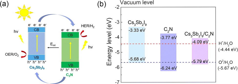
The main problem of most semiconductor photocatalysts is the recombination of electrons and holes, which seriously hinders the water splitting reaction. The Cs3Sb2I9/C2N heterostructure is a type-II band alignment, which can overcome this problem by the spatial separation of photogenerated electron–hole pairs. Fig. 5(a) illustrates the schematic diagram of the photogenerated electron–hole transport mechanism at the Cs3Sb2I9/C2N heterostructure interface. The conduction band offset (CBO) and valence band offset (VBO) were calculated to be 0.6 and 0.79 eV, respectively, which would facilitate the migration of photogenerated electrons from the CB of Cs3Sb2I9 to the CB of C2N, and the migration of photogenerated holes from the VB of C2N to the VB of Cs3Sb2I9, which realizes the spontaneous electron–hole separation in space to overcome the recombination of electron–hole pairs. Beyond this, Eint also plays a role in migrating electrons and holes in opposite directions and inhibiting their recombination. Thus, holes are accumulated at the Cs3Sb2I9 interface and electrons are accumulated in the C2N monolayer. As a consequence, oxygen evolution reaction (OER) chiefly occurs at the Cs3Sb2I9 layer, whereas the hydrogen evolution reaction occurs on the C2N layer. To achieve water splitting, the band-gap of the photocatalyst should be higher than the free energy of water splitting (1.23 eV) and proper band edge positions are also necessary.60 Namely, the CBM must be more positive than the standard reduction potential of H+/H2(VH+/H2), and the VBM must be more negative than the standard oxidation potential of O2/H2O(VO2/H2O). From previous studies (VH+/H2) and (VO2/H2O) are −4.44 eV and −5.67 eV with respect to the vacuum level, respectively.19,61 Hence, based on the vacuum level and the relative positions of the CBM, VBM and Fermi levels, the band edge positions of the CBM and VBM of the monolayer Cs3Sb2I9, C2N and Cs3Sb2I9/C2N heterostructure were obtained according to the HSE06 calculation, as depicted in Fig. 5(b). We can know that the calculated CBM and VBM of the Cs3Sb2I9 monolayer and C2N monolayer both cross the redox potential of water, indicating that they possess water splitting ability. However, the potential of the VBM in the Cs3Sb2I9 monolayer is very close to the O2/H2O potential, which may inhibit the hydrogen production capacity, and the larger band-gap of the C2N monolayer is not conducive to light absorption. For the Cs3Sb2I9/C2N heterostructure, which has a smaller band-gap than the monolayer, the CBM is 0.35 eV higher than that of H+/H2, where the VBM is 0.15 eV lower than that of O2/H2O, and the band configuration is type-II, which shows that the Cs3Sb2I9/C2N heterostructure is favorable for photocatalytic water splitting.
 | ||
| Fig. 5 (a) Schematic illustration of the migration mechanism for photogenerated electron–holes at the interface of the Cs3Sb2I9/C2N heterostructure. (b) The band edge positions of the CBM and VBM of the Cs3Sb2I9, C2N monolayer and Cs3Sb2I9/C2N heterostructure were obtained according to the HSE06 calculations. The vacuum level is set to zero. | ||
Applying external strain has been recognized as an efficient way to tune the electronic, optical, and structural properties of 2D vdW heterostructures, especially the band edge alignment, which is beneficial for photocatalysis, optoelectronics, and nanoelectronic devices.62,63 And it has been demonstrated that tensile or compressive strain is feasible in experiments.64 Here, we systematically investigate the effect of biaxial strain on the strain energy, binding energy, band-gap, band edge position, and optical properties of the Cs3Sb2I9/C2N vdW heterostructure by varying the lattice parameters as follows:
| ε = (a − a0)/a0 | (4) |
| Es = Estrain − Eunstrain | (5) |
 | ||
| Fig. 6 (a) Strain energy (blue line) and band-gap (red line) and (b) binding energy of the Cs3Sb2I9/C2N heterostructure vary with a biaxial strain of −6% to 6%. (c) The band edge positions of the Cs3Sb2I9/C2N heterostructure under different biaxial strains. | ||
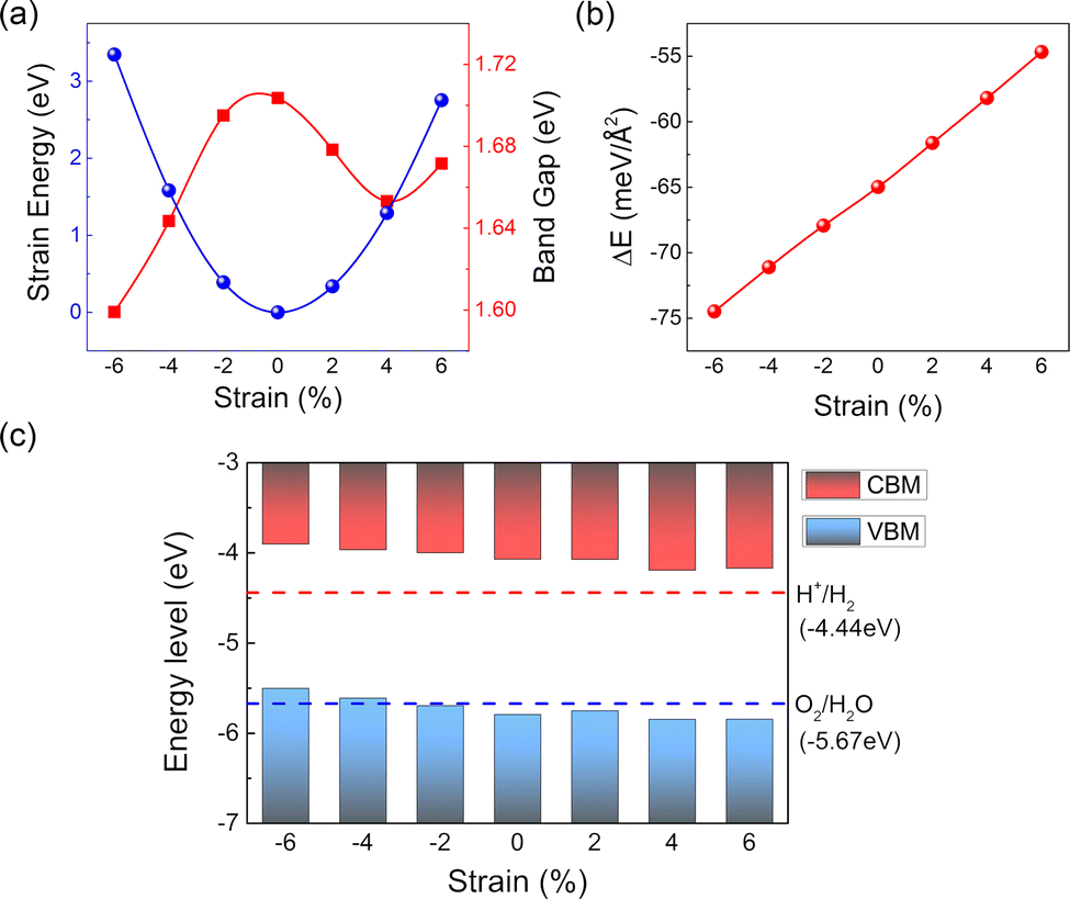
After verifying the reversibility and stability of the structure, the band-gap change of the Cs3Sb2I9/C2N vdW heterostructure with biaxial strain is also depicted in Fig. 6(a) (see red line), and the band structures under different strains are shown in Fig. S2 (ESI†). It can be seen that the band-gap gradually decreases as the compressive strain varies from −2% to −6%. When the applied tensile strain is changed from 0% to 4%, the band-gap first decreases, and then when it reaches 6%, the band-gap starts to increase again. However, in the whole process of applying −6% to 6% biaxial strain, the change of the band-gap value is not significant, indicating that the heterostructure has a good buffering effect on the strain. On the other hand, the indirect band-gap properties of the Cs3Sb2I9/C2N heterostructure remain unchanged in the applied biaxial strain range of −6% to 6%, and its VBM is always located at the Γ and K points, while the CBM appears at the Γ point. The behavior of type-II band alignment was persistent throughout the process.
Fig. 6(c) shows the band edge changes of the Cs3Sb2I9/C2N heterostructure under various biaxial strains. Obviously, with increasing compressive strain, the CBM gradually moved away from the water reduction level and the VBM gradually approached the oxidation level. This means that the water reducing ability of the system gradually increases, while the oxidizing ability becomes weaker, which is not conducive to the production of oxygen. When the compressive strain is increased to −4%, the Cs3Sb2I9/C2N heterostructure is only suitable for hydrogen evolution but not for oxygen evolution. In contrast, the Cs3Sb2I9/C2N heterostructure consistently exhibited photocatalytic water splitting properties when the strain was varied from 2% to 6%.
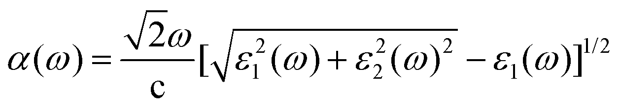
The optical absorption is a characteristic that must be considered in the field of photocatalysis, and broad and strong light absorption is an indispensable factor to achieve efficient solar energy conversion and obtain high photocatalytic activity. With this in mind, the optical absorption coefficients of Cs3Sb2I9, C2N monolayer and Cs3Sb2I9/C2N heterostructure were calculated using the HSE06 method. The optical absorption coefficient can be represented by the following equation:65
 | (6) |
Fig. 7 shows the optical absorption spectra as a function of photon energy for the Cs3Sb2I9 monolayer, the C2N monolayer, and the Cs3Sb2I9/C2N heterostructure under unstrained and −4%, −6%, +4%, and +6% biaxal strains. It can be found that the light absorption level can reach 105 cm−1, and the absorption performance of the Cs3Sb2I9/C2N heterostructure in the visible light range is superior to that of the Cs3Sb2I9 and C2N monolayers. First, the optical absorption of the Cs3Sb2I9/C2N heterostructure is significantly enhanced. This can be attributed to the effect of the charge transfer and interlayer coupling between the two monolayers, which can lead to overlapping electronic states in the valence bands of the heterostructure.66 In addition, due to the smaller band-gap of the Cs3Sb2I9/C2N heterostructure, the optical absorption edge is red-shifted compared with the monolayer, broadening the absorption of visible light. When compressive strains of −4% and −6% are applied, the absorption edge of the spectrum is significantly further red-shifted than when no strain is applied, which is consistent with the variation of its band-gap. But when the compressive strain reaches −6%, the overall light absorption coefficient becomes lower than that without strain. Conversely, with a tensile strain from 4% to 6%, the absorption spectrum undergoes a slight blue-shift, and the intensity of the first absorption peak is significantly enhanced. These results demonstrate that the Cs3Sb2I9/C2N heterostructure not only possesses excellent optical properties, but also that its optical properties can be effectively tuned by biaxial strain and maintain a consistently high absorption coefficient. Therefore, the Cs3Sb2I9/C2N vdW heterostructure is more efficient in harnessing solar energy, which holds great promise in the field of visible light harvesting photocatalysis.
 | ||
| Fig. 7 The absorption coefficients of the Cs3Sb2I9 and C2N monolayers, and the Cs3Sb2I9/C2N heterostructure under different strains. | ||
Conclusions
In summary, using first principles calculations, we systematically explored the stability, electronic and optical properties, and effects of applied biaxial strain on the Cs3Sb2I9/C2N heterostructure to explore its ability as a water splitting photocatalyst. The results show that the Cs3Sb2I9/C2N vdW heterostructure has satisfactory dynamic and thermal stability, and exhibits the characteristics of type-II band alignment in the equilibrium configuration, which is beneficial for the separation of photogenerated carriers. The charge transfer mechanism was analyzed by charge density difference and work function, which further proves the separation of charge, and Bader charge indicated that the electrons of 0.049|e| migrated from Cs3Sb2I9 to the C2N monolayer. In addition, the built-in electric field Eint around the interfacial region further suppresses electron–hole pair recombination. More importantly, appropriate band-gap and band edge positions of the Cs3Sb2I9/C2N heterostructure allow it to realize photocatalytic water splitting. And it exhibits enhanced light absorption capability in the visible light region. Furthermore, the electronic and optical properties of the Cs3Sb2I9/C2N heterostructure can be tuned by strain, and the Cs3Sb2I9/C2N heterostructure always possesses photocatalytic ability after applying −2% to 6% biaxial strains. We hope that the obtained results can provide useful guidance for experimentalists to design efficient photocatalysts for water splitting.Conflicts of interest
The authors declare no competing financial interest.Acknowledgements
This work was partially supported by the National Natural Science Foundation of China (No. 11704282), Natural Science Foundation of Tianjin City (No. 18JCQNJC72900), and Education Commission Research Project of Tianjin City (No. 2017KJ251).References
- G. Kumar, S. H. Kim, C. H. Lay and V. K. Ponnusamy, Bioresour. Technol., 2020, 317, 124010 CrossRef CAS PubMed.
- H. Wang, L. Zhang, Z. Chen, J. Hu, S. Li, Z. Wang, J. Liu and X. Wang, Chem. Soc. Rev., 2014, 43, 5234–5244 RSC.
- Y. Rao, F. Zhang, B. Zhu, H. Li, K. Zheng, Y. Zou, X. Feng, H. Guo, J. Qiu, X. Chen and J. Yu, New J. Chem., 2021, 45, 13571–13578 RSC.
- T. Hisatomi, J. Kubota and K. Domen, Chem. Soc. Rev., 2014, 43, 7520–7535 RSC.
- Z. Wang, C. Li and K. Domen, Chem. Soc. Rev., 2019, 48, 2109–2125 RSC.
- A. Fujishima and K. Honda, Nature, 1972, 238, 37–38 CrossRef CAS PubMed.
- A. R. Amani-Ghadim, F. Khodam and M. S. Seyed Dorraji, J. Mater. Chem. A, 2019, 7, 11408–11422 RSC.
- V. Etacheri, R. Roshan and V. Kumar, ACS Appl. Mater. Interfaces, 2012, 4, 2717–2725 CrossRef CAS PubMed.
- M. Higashi, K. Domen and R. Abe, J. Am. Chem. Soc., 2012, 134, 6968–6971 CrossRef CAS PubMed.
- X. Ning and G. Lu, Nanoscale, 2020, 12, 1213–1223 RSC.
- I. M. Szilágyi, B. Fórizs, O. Rosseler, Á. Szegedi, P. Németh, P. Király, G. Tárkányi, B. Vajna, K. Varga-Josepovits, K. László, A. L. Tóth, P. Baranyai and M. Leskelä, J. Catal., 2012, 294, 119–127 CrossRef.
- X. P. Wu, I. Choudhuri and D. G. Truhlar, Energy Environ. Mater., 2019, 2, 251–263 CrossRef CAS.
- P. Kumari, N. Bahadur, L. Kong, L. A. O’Dell, A. Merenda and L. F. Dumée, Mater. Adv., 2022, 3, 2309–2323 RSC.
- P. Garg, S. Kumar, I. Choudhuri, A. Mahata and B. Pathak, J. Phys. Chem. C, 2016, 120, 7052–7060 CrossRef CAS.
- H. L. Zhuang, M. D. Johannes, M. N. Blonsky and R. G. Hennig, Appl. Phys. Lett., 2014, 104, 022116 CrossRef.
- X. Lv, W. Wei, Q. Sun, F. Li, B. Huang and Y. Dai, Appl. Catal., B, 2017, 217, 275–284 CrossRef CAS.
- S. Zhang, H. Jin, C. Long, T. Wang, R. Peng, B. Huang and Y. Dai, J. Mater. Chem. A, 2019, 7, 7885–7890 RSC.
- A. K. Singh, K. Mathew, H. L. Zhuang and R. G. Hennig, J. Phys. Chem. Lett., 2015, 6, 1087–1098 CrossRef CAS PubMed.
- H. L. Zhuang and R. G. Hennig, Chem. Mater., 2013, 25, 3232–3238 CrossRef CAS.
- Q. Lu, Y. Yu, Q. Ma, B. Chen and H. Zhang, Adv. Mater., 2016, 28, 1917–1933 CrossRef CAS PubMed.
- D. Voiry, J. Yang and M. Chhowalla, Adv. Mater., 2016, 28, 6197–6206 CrossRef CAS PubMed.
- C. Chowdhury, S. Karmakar and A. Datta, J. Phys. Chem. C, 2017, 121, 7615–7624 CrossRef.
- Z. Guo, J. Zhou, L. Zhu and Z. Sun, J. Mater. Chem. A, 2016, 4, 11446–11452 RSC.
- C. F. Fu, X. Li, Q. Luo and J. Yang, J. Mater. Chem. A, 2017, 5, 24972–24980 RSC.
- X. Du, X. Bai, L. Xu, L. Yang and P. Jin, Chem. Eng. J., 2020, 384, 123245 CrossRef CAS.
- L. Xu, Z. Ma, Q. Li, T. Chen, B. Peng, J. Zeng, Y. Zhang, K. W. Luo, L.-L. Wang and C. Shuai, New J. Chem., 2020, 44, 15439–15445 RSC.
- Z. Zhang, Y. Zhang, Z. Xie, X. Wei, T. Guo, J. Fan, L. Ni, Y. Tian, J. Liu and L. Duan, Phys. Chem. Chem. Phys., 2019, 21, 5627–5633 RSC.
- S. J. Hong, S. Lee, J. S. Jang and J. S. Lee, Energy Environ. Sci., 2011, 4, 1781–1787 RSC.
- B. J. Wang, X. H. Li, X. L. Cai, W. Y. Yu, L. W. Zhang, R. Q. Zhao and S.-H. Ke, J. Phys. Chem. C, 2018, 122, 7075–7080 CrossRef CAS.
- H. T. T. Nguyen, T. V. Vu, V. T. Pham, N. N. Hieu, H. V. Phuc, B. D. Hoi, N. T. T. Binh, M. Idrees, B. Amin and C. V. Nguyen, RSC Adv., 2020, 10, 2967–2974 RSC.
- Y. Guan, X. Li, R. Niu, N. Zhang, T. Hu and L. Zhang, Nanomaterials, 2020, 10, 2037 CrossRef CAS PubMed.
- H. Qiao, Y. Zhang, Z. H. Yan, L. Duan, J. B. Fan and L. Ni, Surf. Sci., 2022, 723, 122103 CrossRef CAS.
- R. Kumar, D. Das and A. K. Singh, J. Catal., 2018, 359, 143–150 CrossRef CAS.
- J. Mahmood, E. K. Lee, M. Jung, D. Shin, I. Y. Jeon, S. M. Jung, H. J. Choi, J. M. Seo, S. Y. Bae, S. D. Sohn, N. Park, J. H. Oh, H. J. Shin and J. B. Baek, Nat. Commun., 2015, 6, 6486 CrossRef CAS PubMed.
- R. Zhang, B. Li and J. Yang, Nanoscale, 2015, 7, 14062–14070 RSC.
- S. Guan, Y. Cheng, C. Liu, J. Han, Y. Lu, S. A. Yang and Y. Yao, Appl. Phys. Lett., 2015, 107, 231904 CrossRef.
- X. Luo, G. Wang, Y. Huang, B. Wang, H. Yuan and H. Chen, Phys. Chem. Chem. Phys., 2017, 19, 28216–28224 RSC.
- W. Wei and T. Jacob, Phys. Rev. B, 2013, 87, 085202 CrossRef.
- L. A. Zemnukhova, G. A. Fedorishcheva and R. L. Davidovich, Z. Naturforsch., 2000, 55, 134–138 CrossRef CAS.
- B. Saparov, F. Hong, J. P. Sun, H. S. Duan, S. Cameron, I. G. Hill, Y. Yan and D. B. Mitzi, Chem. Mater., 2015, 27, 5622–5632 CrossRef CAS.
- Y.-L. Liu, C.-L. Yang, M.-S. Wang, X.-G. Ma and Y.-G. Yi, J. Mater. Sci., 2018, 54, 4732–4741 CrossRef.
- H. Li, T. Luo, S. Zhang, Z. Sun, X. He, W. Zhang and H. Chang, Energy Environ. Mater., 2020, 4, 46–64 CrossRef.
- P. C. Harikesh, H. K. Mulmudi, B. Ghosh, T. W. Goh, Y. T. Teng, K. Thirumal, M. Lockrey, K. Weber, T. M. Koh, S. Li, S. Mhaisalkar and N. Mathews, Chem. Mater., 2016, 28, 7496–7504 CrossRef CAS.
- L. Mao, C. C. Stoumpos and M. G. Kanatzidis, J. Am. Chem. Soc., 2019, 141, 1171–1190 CrossRef CAS PubMed.
- D. Cortecchia, H. A. Dewi, J. Yin, A. Bruno, S. Chen, T. Baikie, P. P. Boix, M. Gratzel, S. Mhaisalkar, C. Soci and N. Mathews, Inorg. Chem., 2016, 55, 1044–1052 CrossRef CAS PubMed.
- L. Qian, Y. Sun, M. Wu, C. Li, D. Xie, L. Ding and G. Shi, Nanoscale, 2018, 10, 6837–6843 RSC.
- G. Kresse and J. Hafner, Phys. Rev. B: Condens. Matter Mater. Phys., 1993, 47, 558–561 CrossRef CAS PubMed.
- G. Kresse, J. Furthmuller and J. Hafner, Phys. Rev. B: Condens. Matter Mater. Phys., 1994, 50, 13181–13185 CrossRef CAS PubMed.
- G. Kresse and D. Joubert, Phys. Rev. B: Condens. Matter Mater. Phys., 1999, 59, 1758–1775 CrossRef CAS.
- P. E. Blochl, Phys. Rev. B: Condens. Matter Mater. Phys., 1994, 50, 17953–17979 CrossRef PubMed.
- S. Grimme, J. Antony, S. Ehrlich and H. Krieg, J. Chem. Phys., 2010, 132, 154104 CrossRef PubMed.
- J. Paier, M. Marsman, K. Hummer, G. Kresse, I. C. Gerber and J. G. Angyan, J. Chem. Phys., 2006, 124, 154709 CrossRef CAS PubMed.
- A. Togo, F. Oba and I. Tanaka, Phys. Rev. B: Condens. Matter Mater. Phys., 2008, 78, 134106 CrossRef.
- A. Togo and I. Tanaka, Scr. Mater., 2015, 108, 1–5 CrossRef CAS.
- Y. Chen and J. Washburn, Phys. Rev. Lett., 1996, 77, 4046–4049 CrossRef CAS PubMed.
- X. Zhang, A. Chen, Z. Zhang, M. Jiao and Z. Zhou, Nanoscale Adv., 2019, 1, 154–161 RSC.
- F. Opoku, S. O.-B. Oppong, N. K. Asare-Donkor, O. Akoto and A. A. Adimado, Energy Adv., 2022, 1, 146–158 RSC.
- J. Song, H. Zheng, M. Liu, G. Zhang, D. Ling and D. Wei, Phys. Chem. Chem. Phys., 2021, 23, 3963–3973 RSC.
- H. Zhou, W. Cai, J. Li, X. Liu, W. Xiong, Y. Zhou, Z. Xu, B. Wang and C. Ye, Phys. Chem. Chem. Phys., 2020, 22, 1485–1492 RSC.
- A. K. Singh, K. Mathew, H. L. Zhuang and R. G. Hennig, J. Phys. Chem. Lett., 2015, 6, 1087–1098 CrossRef CAS PubMed.
- V. Chakrapani, J. C. Angus, A. B. Anderson, S. D. Wolter, B. R. Stoner and G. U. Sumanasekera, Science, 2007, 318, 1424–1430 CrossRef CAS PubMed.
- Y. Chen, Q. Sun and P. Jena, J. Mater. Chem. C, 2016, 4, 6353–6361 RSC.
- X. Qian, L. Fu and J. Li, Nano Res., 2014, 8, 967–979 CrossRef.
- Y. Jiao, L. Zhou, F. Ma, G. Gao, L. Kou, J. Bell, S. Sanvito and A. Du, ACS Appl. Mater. Interfaces, 2016, 8, 5385–5392 CrossRef CAS PubMed.
- C. Shao, K. Ren, Z. Huang, J. Yang and Z. Cui, Front. Chem., 2022, 10, 847319 CrossRef CAS PubMed.
- B. Zhou, A. Cui, L. Gao, K. Jiang, L. Shang, J. Zhang, Y. Li, S. J. Gong, Z. Hu and J. Chu, Phys. Rev. B, 2021, 5, 125404 CAS.
Footnote |
| † Electronic supplementary information (ESI) available. See DOI: https://doi.org/10.1039/d2cp04665b |
| This journal is © the Owner Societies 2023 |