
 Open Access Article
 This Open Access Article is licensed under a
 Creative Commons Attribution 3.0 Unported Licence
2D graphitic-like gallium nitride and other structural selectivity in confinement at the graphene/SiC interface†
Gianfranco
Sfuncia
 a,
Giuseppe
Nicotra
*a,
Filippo
Giannazzo
a,
Béla
Pécz
b,
Gueorgui Kostov
Gueorguiev
c and
Anelia
Kakanakova-Georgieva
*c
a,
Giuseppe
Nicotra
*a,
Filippo
Giannazzo
a,
Béla
Pécz
b,
Gueorgui Kostov
Gueorguiev
c and
Anelia
Kakanakova-Georgieva
*c
aConsiglio Nazionale delle Ricerche, Istituto per la Microelettronica e Microsistemi, Strada VIII, n. 5, Zona Industriale, I-95121, Catania, Italy. E-mail: giuseppe.nicotra@cnr.it
bHUN-REN Centre for Energy Research, Institute of Technical Physics and Materials Science, Konkoly-Thege M. út 29-33, Budapest, 1121, Hungary
cDepartment of Physics, Chemistry and Biology (IFM), Linköping University, 581 83 Linköping, Sweden. E-mail: anelia.kakanakova@liu.se
First published on 7th September 2023
Abstract
Beyond the predictions routinely achievable by first-principles calculations and using metal–organic chemical vapor deposition (MOCVD), we report a GaN monolayer in a buckled geometry obtained in confinement at the graphene/SiC interface. Conductive atomic force microscopy (C-AFM) was used to investigate vertical current injection across the graphene/SiC interface and to establish the uniformity of the intercalated regions. Scanning transmission electron microscopy (S/TEM) was used for atomic resolution imaging and spectroscopy along the growth direction. The experimentally obtained value of the buckling parameter, 1.01 ± 0.11 Å, adds to the existing knowledge of buckled GaN monolayers, which is based solely on predictive first-principles calculations. Our study reveals a discontinuity in the anticipated stacking sequence attributed to a few-layer graphitic-like GaN structure. Instead, we identify an atomic order suggestive of ultrathin gallium oxide Ga2O3, whose formation is apparently mediated by dissociative adsorption of oxygen onto the GaN monolayer.
Introduction
The honeycomb monolayer structure of group III nitrides, as well as other group III–V semiconductors, has been substantially investigated by first-principles calculations based on density functional theory.1–3 A few honeycomb monolayers – each with planar trigonal sp2 coordination between group III and nitrogen atoms – stacked in an ultrathin graphitic-like structure are considered as the ultimate scaling down for AlN, GaN and InN. Instead, their 3D bulk is represented by a wurtzite structure with tetrahedral sp3 coordination between atoms. From an alternative perspective, the ultrathin few-layer films of graphitic-like group III nitrides are perceived as acting as precursors to respective thin films with a wurtzite structure.4 For a graphical representation of wurtzite and planar graphitic-like structures attributed to GaN and other semiconductors including AlN, SiC, ZnO, see Fig. 2 in ref. 4. Further predictive first-principles calculations on the structural and electronic properties of few-layer graphitic-like AlN5,6 and GaN7,8 have been selected here.Following predictive first-principles calculations based on both geometry optimization and verification of dynamic stability by phonon dispersion simulations, GaN (together with AlN and InN) was found to form stable planar honeycomb monolayers and stable planar bi-layer AA′ stacking configurations (i.e., hexagons on top of each other with a Ga atom over a N atom and a N atom over a Ga atom).
The stability of the planar graphitic-like structure of GaN was further discussed. Its spontaneous reconstruction into a structure that “remains hexagonal in plane, but with covalent intermediate bonds that form alternating octagonal and square (8|4 Heckelite) rings” has been proposed.9 For example, planar three-layer graphitic-like GaN was found to represent a structure at a saddle point unlike the Haeckelite-type structure which was found to represent a local minimum of the potential energy.9 We note the calculated energy barrier of only 0.15 eV (∼3.45 kcal mol−1) between the graphitic-like and Haeckelite-type structures.9 In principle, such a small barrier is not energetically significant. Even more, any energy barrier less than 40–50 kcal mol−1 is considered as relatively low and in the accessible energy range under MOCVD conditions of group III nitrides.10–12 Therefore, we can highlight the dominant role played by deposition kinetics in the stabilization of various multilayer GaN structures under MOCVD conditions in the presence of a substrate and/or in a confined space, even if they may not represent any local minimum of the potential energy.
By investigating different stacking configurations by predictive first-principles calculations, it was reported that planar graphitic-like AlN can form energetically stable few-layer stacks with graphene.5 Carrying out relaxations of the different stacking configurations, it was found that some deviation in the range of 0.01–0.1 Å of both graphitic-like AlN and graphene monolayers from their planarity can occur.5 Such a small deviation from planarity is perceived to have accommodated any long-range interlayer interactions between graphitic-like AlN and graphene, but it is unrelated to the common buckling parameter.
In general, group III and group V atoms (which form the honeycomb structure of a III–V monolayer) may lie in different planes and therefore exhibit a certain buckling distance. A buckling distance in the range of 0.4–0.7 Å was calculated in the case of a low-buckled honeycomb monolayer geometry which was attributed to common group III–V semiconductors such as InP, InAs, InSb, GaP and GaAs.1 On the other hand, the stable planar honeycomb monolayer structure has been assigned to group III nitrides (and all other binary compounds which contain B and C atoms) by first-principles calculations.1,2 For a graphical representation of the top and side views of a 2D planar and low-buckled honeycomb structure, see Fig. 1 in ref. 1. By stacking planar honeycomb monolayers, it is possible to construct not only stable planar few-layer graphitic-like AlN5,6 and GaN,7,8 but also multilayer 3D graphitic-like structures of AlN,6 and even newly predicted 3D periodic structures of GaN.8 In the latter case,8 the buckled geometry with the associated onset of vertical Ga–N bonds between monolayers was discussed in detail. Noteworthily, the study in ref. 8 points out the “minute” energy difference between the planar bi-layer graphitic-like structure of GaN and other predicted buckled bi-layer structures. Therefore, the dominant effect of deposition kinetics on the stabilization of various multilayer GaN structures under MOCVD conditions in the presence of a substrate and/or in a confined space can be reiterated.
The stability of the planar graphitic-like structure of GaN was further discussed in relation to the extent of passivation of any unsaturated states. Thus, upon complete hydrogen passivation, monolayer and few-layer GaN have been investigated by predictive first-principles calculations and found to be energetically more stable in a buckled geometry.13,14
Here, beyond the predictions routinely achievable by first-principles calculations, we report a GaN monolayer in a buckled geometry obtained in confinement at the graphene/SiC interface by MOCVD processes. Experimentally, the MOCVD of the intercalated GaN structure in this study was performed in a hydrogen carrier gas flow, as were the intercalated structures of 2D AlN15 and 2D InN16 in our previous studies. Trace impurities as oxygen are present in the gas stream at less than 0.5 vol ppm. Nonetheless, the formation of any Ga–O bonds, mediated by dissociative adsorption of oxygen onto the GaN monolayer, may still be relevant and cause structural selectivity to be triggered at the atomic size scale. Our study exposes a discontinuity in the anticipated stacking sequence attributed to a few-layer graphitic-like GaN structure which is argued to be a case of Ga–O bond formation. On the one hand, the formation of Ga–O bonds may have implications for achieving a few-layer graphitic-like GaN. On the other hand, the formation of Ga–O bonds acquires importance in instigating chemical-species-specific structural selectivity in confinement at the atomic size scale.
Experimental
The MOCVD processes were performed in a horizontal-type hot-wall MOCVD reactor (GR508GFR Aixtron) using epitaxial graphene on nominally on-axis 4H-SiC (0001) substrates. The reactor was operated at an H2 flow rate of 25 slm and a pressure of 200 mbar. Trimethylgallium, (CH3)3Ga, and ammonia, NH3, precursors were used at flow rates of 0.442 sccm and 2 slm, respectively. The precursor delivery scheme involved a total of 3 cycles, each of about 3 minutes and consisting of alternating flows of (CH3)3Ga with NH3 followed by an additional time of 10 minutes of their co-delivery. The flow of NH3 and H2 continued during the cooling down stage of the overall MOCVD process. The deposition of GaN was performed at two different temperatures, 700 °C and 1100 °C.The morphology of the samples was evaluated by tapping mode atomic force microscopy (AFM) using Si probes and a DI3100 equipment with a Nanoscope V controller. Conductive atomic force microscopy (C-AFM) was further employed to probe vertical current injection through the graphene/SiC interface. Current mapping was carried out using Pt-coated Si tips with 5 nm curvature radius.
Transmission electron microscopy (TEM) was performed to define both structural and chemical details of the ultrathin films. The TEM lamella was cut by focused ion beam (FIB) in which the energy of Ga ions was reduced to 2 keV using a dual beam FEI SCIOS2 equipment and initial observations were carried out using an FEI THEMIS 200 microscope equipped with an image corrector at 200 keV. Scanning transmission electron microscopy (S/TEM) was carried out in a probe corrected JEOL ARM 200F microscope. High Angle Annular Dark Field (HAADF) S/TEM, with collection angles from 68 to 280 mrad, was used to acquire Z-contrast images (which show an intensity dependence proportional to the atomic number as Z2) highlighting the presence of atomic Ga planes intercalated between bulk SiC and graphene, and to make direct measurements of interlayer distances at the Ångström scale.17 The Annular Bright Field (ABF) S/TEM method was applied by collecting the electrons within a ring-shaped circumference from 11 to 24 mrad cutting the central part of the bright field disk out. The ABF method enables the effective visualization of atomic columns composed simultaneously of heavy and light atoms.18 Electrons of the beam scattered at higher angles, due to the interaction with the heavy atomic columns (high-Z), fall outside of the ABF detector with respect to the lighter ones (lower-Z). The heavy atoms are imaged as dark spots thus allowing even the lightest atoms, otherwise showing very weak contrast, to be visualized. Overall, the ABF method allows the measurement of the buckling distance which is not achievable with other characterization techniques.
Chemical analysis was performed with a TEM post-column Gatan Quantum ER electron energy loss spectrometer (EELS) with an energy resolution of 0.3 eV operated in dual EELS mode which allows simultaneous acquisition of spectra in the zero loss and high energy loss regions. The spectrum imaging (SI) mode, by combining energy dispersive X-ray spectroscopy (EDS) and electron energy loss spectroscopy (EELS) pixel by pixel on the S/TEM image, was also used.
Results and discussion
The overall intercalation process at the graphene/SiC interface under the applied MOCVD conditions obeys several key features. The graphene/SiC interface was obtained in a high-temperature sublimation process and is therefore associated with high energy.19 It is considered to result from the partial bonding of zero-layer graphene to the outermost Si atoms on the SiC surface (every third carbon atom in the zero-layer graphene forms a C–Si bond with the substrate20), and the prevailing large density of unsaturated Si dangling bonds. In general, the graphene/SiC interface may achieve surfaces of reduced energy via the process of hydrogen intercalation and associated regular termination of Si dangling bonds by hydrogen atoms.21 Such a confined space of energy-reduced surfaces has been shown to allow lateral migration of (metal) atoms over large areas and the synthesis of structures with atom-size thickness.19 The approach was first demonstrated in achieving an ultrathin 2D GaNx structure with rhombohedral symmetry confined between graphene and SiC by MOCVD.13 By extending this approach, 2D AlN15 and 2D InN16 by MOCVD have also been reported with very high SiC surface coverage.16The MOCVD processes typically involve trimethyl-based metal–organic precursors such as (CH3)3Al, (CH3)3Ga, and (CH3)3In, which exhibit strong metal–carbon bonding. The average bond strength between the central metal atom (Al, Ga, and In) and the methyl group in these trimethyl-based compounds, obtained from ab initio calculations according to their fragmentation shows a value of ∼82.3, 79.4, and 66.8 kcal mol−1, respectively.22 Therefore, the efficiency of the dissociative adsorption of these strongly bonded metal–organic precursors, which enables the delivery of individual metal adatoms onto the graphene surface, ultimately determines the efficiency of the intercalation process. We have, for example, identified (CH3)3In/graphene reaction pathways using ab initio molecular dynamics simulations that involve SiC-supported graphene in a H2 environment and promoted a better understanding of the relevant mechanisms that regulate the MOCVD processes at the atomic scale.23
Alternatively, in a typical intercalation approach – which involves deposition of metal atoms on graphene followed by annealing in an ultra-high vacuum system in the absence of hydrogen (see for example ref. 24 about intercalated In) – the high energy of the zero-layer graphene/SiC interface can act as a thermodynamic force to intercalate metal atoms beneath the zero-layer graphene and minimize the interfacial energy.25,26 The observed “spontaneous” intercalation of Ga (along with In) atoms reported in ref. 25 resulted from plasma-assisted molecular beam epitaxy growth of GaN on graphene on SiC, while the intercalation of In and Ga atoms (along with Sn atoms) reported in ref. 26 is the result of a vaporization of metallic precursors situated in a crucible underneath the epitaxial graphene. A common feature in these intercalation processes24–26 is the availability of free atoms of In and Ga.
As described in the Experimental part, the precursors, (CH3)3Ga and NH3, were fed into the MOCVD reactor following a specific scheme at two different temperatures of 700 and 1100 °C. We selected the temperature of 700 °C considering the previous successful intercalation of AlN15 and InN16 at the graphene/SiC interface by MOCVD in the same reactor and at the same temperature of 700 °C. An intercalation temperature of 1100 °C was selected for the second set of experimental data because a temperature near 1100 °C is commonly used for epitaxy of GaN on SiC. Following the findings in the present study, we can confirm that a temperature around 700 °C – and in relation to the other established parameters of the MOCVD reactor, the precursor feeding scheme and the characteristics of the graphene template – provided conditions for successful intercalation of group III nitrides in general and for probing a part of the landscape of group III nitrides at the 2D limit.
Initially, the samples were characterized by conductive AFM (C-AFM). Particularly, current maps obtained by C-AFM can provide local information on the electronic transport across the graphene/SiC heterojunction with a lateral resolution corresponding to the effective contact size of the metallic tip (curvature radius of ∼5 nm). A schematic of the employed experimental set-up is reported in Fig. 1a. Two morphological images of the epitaxial graphene on SiC after intercalation at 700 °C and 1100 °C are shown in Fig. 1b and c, respectively. Furthermore, the corresponding current maps measured on the two sample regions are reported in Fig. 1d and e.
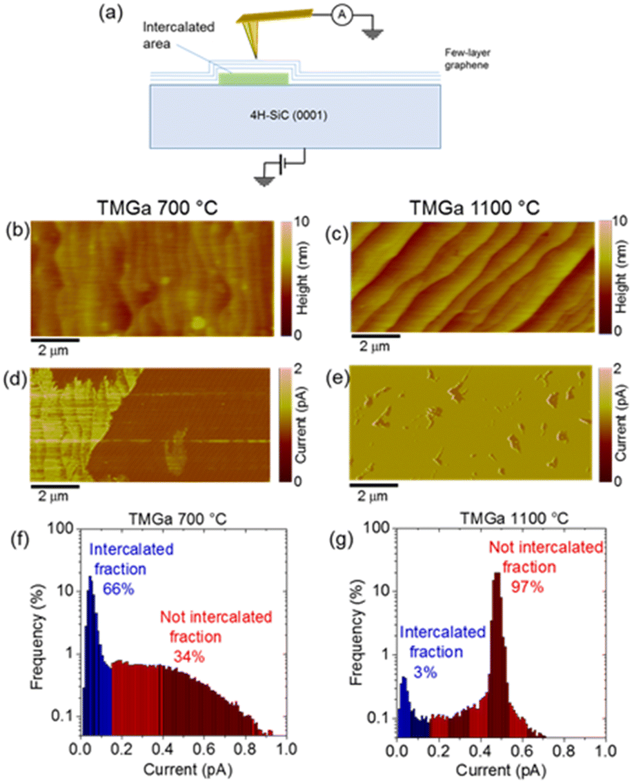 | ||
| Fig. 1 (a) Schematic of the C-AFM setup for vertical current mapping through the intercalated and non-intercalated interfaces. Surface morphology of epitaxial graphene on 4H-SiC after intercalation at 700 °C (b) and 1100 °C (c). Corresponding current maps on the same sample areas ((d) and (e)). Histograms of current distributions on the two samples ((f) and (g)), from which the percentage of intercalated areas was estimated. | ||
Surface topography is very similar for the two samples, and it exhibits the typical step-bunching of a 4H-SiC substrate, arising from the high temperature used for graphene formation. On the other hand, significant differences can be observed between the two current maps, indicating a very different homogeneity of the intercalation at the graphene/SiC interface at the two MOCVD temperatures. As recently demonstrated also in the case of intercalated InN,16 the presence of an ultrathin barrier layer causes a reduction of the injected current with respect to non-intercalated graphene/SiC areas. While uniformly intercalated areas (low current contrast) separated by non-intercalated ones (high current contrast) can be observed in the sample subjected to intercalation at 700 °C (Fig. 1d), the 1100 °C MOCVD process results in the formation of small size intercalated patches (see Fig. 1e) surrounded by non-intercalated regions. Finally, the percentage of intercalated areas has been quantitatively estimated from the histogram of current distribution extracted from the two current maps reported in Fig. 1f and g, respectively. Both distributions exhibit a peak at low currents associated with the intercalated regions of the sample. The sum of counts under these peaks corresponds to the intercalated surface fractions. Hence, we could evaluate up to 66% intercalation after the 700 °C MOCVD and only 3% intercalation after the 1100 °C process. The occurrence of the Ga intercalation at the graphene/SiC interface should be directly related to the dissociative adsorption of the (CH3)3Ga precursor and the surface reactions of the (CH3)3Ga precursor with graphene under the applied MOCVD conditions.
Heating graphene/SiC in hydrogen to a high temperature of 1100 °C (compared to heating to a lower temperature of 700 °C) is expected to lead to a more complete detachment of the zero-layer graphene from the Si-terminated SiC surface and its transformation in the 1st layer of graphene. Therefore, the 1100 °C process reduces the areas that expose zero-layer graphene. At the same time, the reactivity of the zero-layer graphene – due to bonding with the underlying Si atoms of the SiC substrate – is expected to facilitate the dissociative adsorption of the (CH3)3Ga precursor and the delivery of Ga adatoms onto the graphene surface (see ref. 23 for the case of atomistic pathways for the supply of In atoms from (CH3)3In precursor to the graphene surface). Therefore, we hypothesize that the smaller percentage of Ga intercalation after the MOCVD process at 1100 °C may be the result of a less efficient dissociative adsorption of the (CH3)3Ga precursor. Expressing the latter observation in another way, a more efficient dissociative adsorption of the (CH3)3Ga precursor – and consequently a further increase in the intercalated area coverage in the 700 °C MOCVD process – can be provided by properly designing zero-layer (only) graphene templates.
HAADF S/TEM images confirmed the intercalation by the presence of a very bright contrast at the graphene/SiC interface, which is related to the presence of Ga atoms with a high atomic number (Z-contrast image). In confirmation of this, Fig. 2a and c show comparative HAADF S/TEM images of intercalated and non-intercalated graphene/SiC interfaces at 700 °C, respectively. Furthermore, a linear intensity profile was extracted for both micrographs after integration over the area in the depicted boxes and used to measure the interplanar atomic distances, Fig. 2b and d. In this way, the characteristic interplanar distance of about 2.5 Å in bulk SiC, and 3.3 Å in bilayer graphene, respectively, can be confirmed, Fig. 2d. The first carbon layer is displaced from the underlying SiC substrate by 2.8 Å, Fig. 2d, and is therefore indicative of its incomplete detachment,17 for which a displacement of about 3.6–3.8 Å is typically expected.27 The spacing of about 2.8–2.9 Å between the intercalated Ga layers beneath a single layer of graphene in this case is accordingly indicated in Fig. 2c.
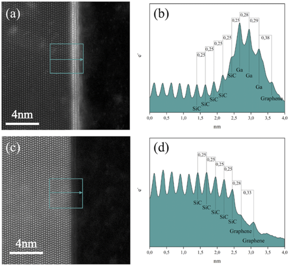 | ||
Fig. 2 HAADF image and linear intensity profile, integrated over the area in the box, of the intercalated (a and b) and non-intercalated (c and d) graphene/SiC interface. Images are acquired near the [11![[2 with combining macron]](https://www.rsc.org/images/entities/char_0032_0304.gif) 0] zone axis. Arrows in the boxes indicate the x-axis direction of intensity profiles. Distances reported in (b) and (d) are expressed in nm. 0] zone axis. Arrows in the boxes indicate the x-axis direction of intensity profiles. Distances reported in (b) and (d) are expressed in nm. | ||
The intercalated layers at the graphene/SiC interface were characterized in the SI mode by combining EDX and EELS spectroscopy for compositional and electronic properties. SI/EDS was used to identify the chemical species of interest, i.e., silicon, gallium, nitrogen, and oxygen, and to produce two-dimensional elemental maps as shown in Fig. 3. EDS analysis shows the contemporary presence of nitrogen and oxygen corresponding to gallium layers. In particular, the nitrogen signal originates closer to the gallium–silicon interface, while the oxygen signal comes from the outer gallium layers.
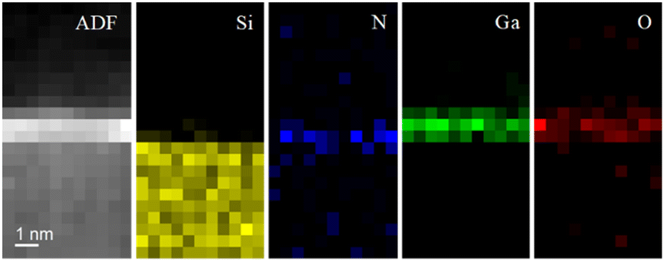 | ||
| Fig. 3 ADF image of intercalated graphene/SiC acquired in the SI mode and correlated EDS bidimensional elemental maps of silicon, nitrogen, gallium, and oxygen. Pixel size is 0.5 × 0.5 nm. | ||
The SI/EELS study provided information on the bonding and oxidation state of Ga in the intercalated structure (Fig. 4). To increase the signal-to-noise ratio (SNR) of the EELS spectra, the counts are integrated within four rectangular boxes along the region of interest, as displayed in the acquired ADF image (Fig. 4a), so that each one encloses the area between two adjacent atomic layers (e.g., the first box between the last atomic layer of silicon and the first of gallium, the second box between the first two atomic layers of gallium); we may safely assume that electronic distribution over the integration area is the same. The four integrated spectra are reported in Fig. 4b and from their examination we obtain the following results. Spectrum 1, the SiC/GaN interface, shows the presence of a nitrogen K-edge peak starting at 400 eV. In spectra 2 and 3, the GaN/GaN interface, the nitrogen signal significantly drops until it disappears in spectrum 4, the GaN/graphene interface. Spectrum 1 also shows the presence of an oxygen K-edge peak near 530 eV, whose intensity increases in spectrum 2, remaining constant in spectra 3 and 4.
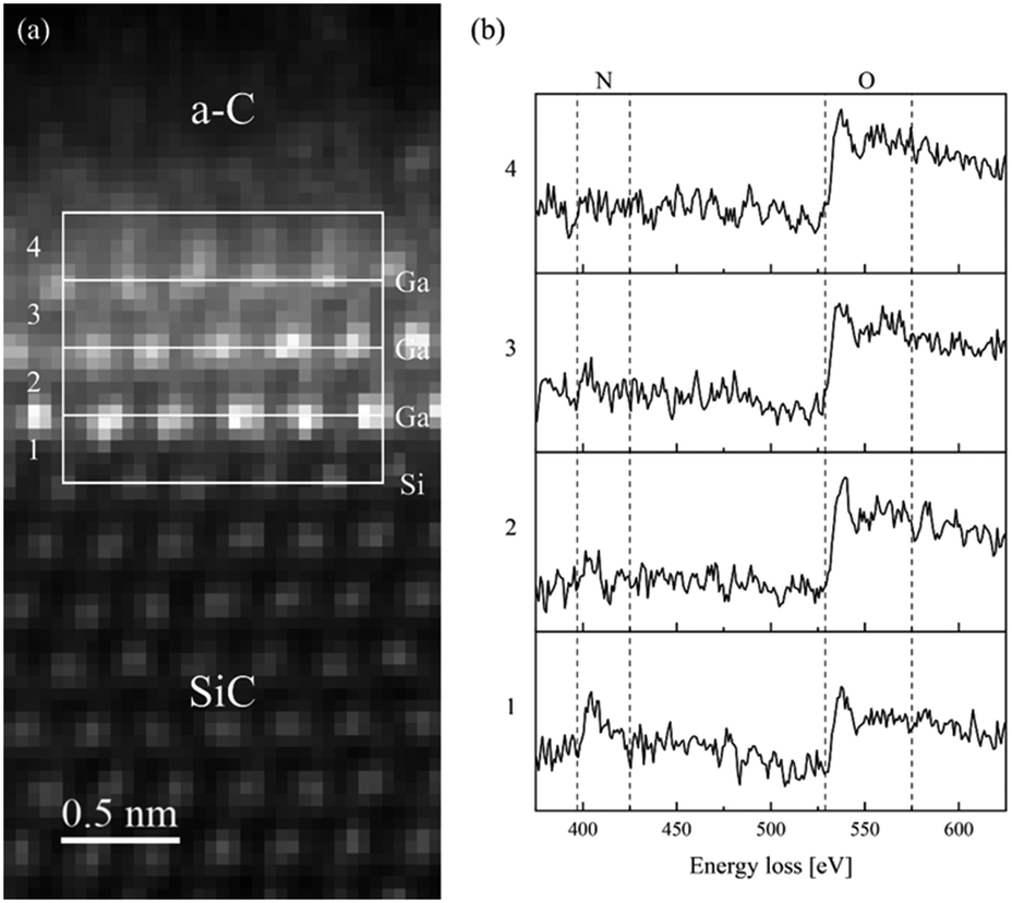 | ||
| Fig. 4 (a) ADF image of intercalated graphene/SiC. (b) Plots of EELS spectra acquired in the SI mode in the high loss region of nitrogen and oxygen K-edge peaks, integrated over the corresponding area within the four different boxes. Pixel size is set at 0.05 × 0.05 nm. Amorphous carbon (a-C) at the top was deposited during FIB preparation of the TEM lamella for surface protection during the milling. | ||
Remarkably, EELS analysis of the studied intercalated structure allowed for the detection of a clear nitrogen signal from a monolayer at the immediate interface with the underlying SiC substrate (spectrum 1 in Fig. 4b). Lighter elements such as N and O were successfully visualized by ABF S/TEM imaging of the atomic order in the studied intercalated structure along with the heavy element Ga (see Fig. 5). The ABF S/TEM image of the atomic order in the studied intercalated structure in conjunction with the EELS analysis of the structure supports the representation of the monolayer, which is immediately adjacent to the SiC surface, as a GaN monolayer with Ga and N atoms occupying certain positions in a buckled geometry. The oxygen peak in spectrum 1 may be related to minor oxygen substitution and/or signal delocalization from the upper layer. In spectra 2 and 3, weaker nitrogen signals together with the prominent oxygen peaks indicate the oxidation of Ga occurring in the two outer atomic layers. SI/EELS spectra were also obtained in bulk 4H-SiC and amorphous carbon deposited during FIB preparation of the TEM lamella to confirm that the recorded EELS oxygen signals through the intercalated structure have at most a negligible contribution from surface oxidation of the sample (Fig. S1†).
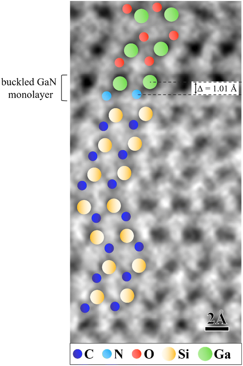 | ||
| Fig. 5 ABF S/TEM image of the atomic order in the investigated intercalated structure. The GaN monolayer at the immediate interface with the underlying SiC substrate has a buckled geometry, which is denoted by the Ga and N atoms lying in different planes with a buckling distance of Δ = 1.01 Å. The Ga atoms in the topmost quintuple have adopted an atomic order suggestive of ultrathin gallium oxide Ga2O3 (see text for more details). We note a stacking order fault in the SiC substrate at the interface with the GaN monolayer (further details in Fig. S2†). | ||
Therefore, the EELS results confirm the successful intercalation of Ga and N between SiC and graphene, while further continuous replacement of nitrogen atoms by oxygen atoms becomes evidently relevant across the intercalated structure and is indicative of the formation of Ga–O bonds. The EELS results were corroborated by ABF S/TEM imaging, which allowed the atomic order in the intercalated structure to be probed by visualizing lighter elements such as nitrogen and oxygen (Fig. 5).
In interpreting the results presented above, we believe that the formation of a confined GaN monolayer at the graphene/SiC interface is the primary process. Its buckled geometry can be indicated by the Ga and N atoms lying in different planes and having a certain buckling distance of Δ = 1.01 ± 0.11 Å (our pixel size is 0.11 Å). Therefore, this experimentally derived value adds to the existing knowledge of buckled honeycomb GaN monolayers, which is based solely on predictive first-principles calculations. The buckling parameter of a free-standing hydrogenated GaN monolayer was calculated as Δ = 0.716 Å.28 Upon formation of a GaN monolayer, adsorption sites favorable for dissociation of, for example, simple traces of O2 impurities can become accessible on its Ga surface by overcoming an energy barrier of only 1.13 eV (∼26.05 kcal mol−1), which finds its reasoning in ab initio calculations.29 Oxygen species are inevitably present in the MOCVD environment as trace amounts of H2O and O2 (<0.5 vol ppm) in the gas stream. Thus, we speculate that the presence of oxygen adatoms under certain conditions may change the bonding environment for (incoming) intercalated Ga atoms and cause a break in the stacking sequence of the uppermost GaN monolayers and the formation of the anticipated stacking sequence attributed to a few-layer graphitic-like GaN structure. Instead, the Ga atoms in the topmost quintuple layer of the studied intercalated structure were found to have adopted an atomic order suggestive of ultrathin gallium oxide Ga2O3. The ultrathin structure of Ga2O3 has been characterized by its Ga atoms occupying sites of both, octahedral and tetrahedral coordination in the O–Ga–O trilayer and Ga–O bilayer, respectively.30 In the example of the established atomic order in the intercalated structure from Fig. 5, we can validate a case of polarity inversion by simultaneous formation of Ga–N and Ga–O bonds.
We can reasonably expect that the incorporation of (trace) impurities such as oxygen into the crystal lattice of (2D) GaN can be affected by tuning the intercalation/deposition kinetics. Tuning the deposition kinetics may, for example, be achieved by tuning the carrier gas flow rate, which in turn affects the residence time of the precursors in the deposition zone to promote, or alternatively suppress, the occurrence of certain gas phases and surface reactions that affect the incorporation of (trace) impurities into the crystal lattice. Recently, various aspects of deposition kinetics have been highlighted in connection with (MO)CVD of other 2D vertical heterostructures based on, for example, binary31 and ternary32 transition metal dichalcogenides.
As to the intricate structural relationship between GaN and Ga2O3, we draw attention to a distinct template approach to crystalline GaN nanosheets. The GaN nanosheets can be obtained through solid diffusion/replacement reaction of γ-Ga2O3 with ammonia gas under a proper nitridation process.33
Conclusions
Beyond the predictions routinely achievable by first-principles calculations and using MOCVD and advanced atomic resolution imaging and spectroscopy, we report a GaN monolayer in a buckled geometry obtained in confinement at the graphene/SiC interface. A discontinuity in the anticipated stacking sequence attributed to a few-layer graphitic-like GaN structure is exposed and reasoned as a case of structural selectivity at the atomic size scale mediated by dissociative adsorption of oxygen onto the GaN monolayer.Author contributions
A. K.-G. developed the MOCVD processes and conceptualization of the manuscript. F. G. performed the C-AFM measurements. B. P. obtained the TEM images. The STEM study and analytical measurements were performed by G. N. and G. S. The manuscript was written with input from all authors.Conflicts of interest
There are no conflicts to declare.Acknowledgements
The authors thank Dr. T. Iakimov and Prof. R. Yakimova for kindly providing epitaxial graphene samples and Dr. C. Bongiono and Dr. A. M. Mio for the helpful discussions. This work was carried out within the framework of the FLAG-ERA GRIFONE project. A. K.-G. acknowledges support from the Swedish Research Council (VR) through project grant VR 2017-04071 and VR 2015–06816. B. P. acknowledges the support of TKP2021-NKTA-05 and VEKOP-2.3.3-15-2016-00002 of the European Structural and Investment Funds. F. G. and B. P. acknowledge the CNR-HAS 2023–2025 GHOST III bilateral project. S/TEM was performed at the BeyondNano CNR-IMM labs, which are supported by the Italian Ministry of Education and Research (MIUR) under the Beyond-Nano project (PON a3_00363). Part of this work received funding from the European Union's Horizon 2020 research and innovation program under grant agreement No. 823717 – ESTEEM3.References
- H. Şahin, S. Cahangirov, M. Topsakal, E. Bekaroglu, E. Akturk, R. T. Senger and S. Ciraci, Monolayer honeycomb structures of group-IV elements and III-V binary compounds: First-principles calculations, Phys. Rev. B: Condens. Matter Mater. Phys., 2009, 80, 155453 CrossRef.
- E. F. de Almeida Junior, F. de Brito Mota, C. M. C. de Castilho, A. Kakanakova-Georgieva and G. K. Gueorguiev, Defects in hexagonal-AlN sheets by first-principles calculations, Eur. Phys. J. B, 2012, 85, 48 CrossRef.
- H. L. Zhuang, A. K. Singh and R. G. Hennig, Computational discovery of single-layer III-V materials, Phys. Rev. B: Condens. Matter Mater. Phys., 2013, 87, 165415 CrossRef.
- C. L. Freeman, F. Claeyssens and N. L. Allan, Graphitic Nanofilms as Precursors to Wurtzite Films: Theory, Phys. Rev. Lett., 2006, 96, 066102 CrossRef PubMed.
- R. B. dos Santos, F. de Brito Mota, R. Rivelino, A. Kakanakova-Georgieva and G. K. Gueorguiev, Van der Waals stacks of few-layer h-AlN with graphene: an ab initio study of structural, interaction and electronic properties, Nanotechnology, 2016, 27, 145601 CrossRef PubMed.
- C. Bacaksiz, H. Sahin, H. D. Ozaydin, S. Horzum, R. T. Senger and F. M. Peeters, Hexagonal AlN: Dimensional-crossover-driven band-gap transition, Phys. Rev. B: Condens. Matter Mater. Phys., 2015, 91, 085430 CrossRef.
- D. Xu, H. He, R. Pandey and S. P. Karna, Stacking and electric field effects in atomically thin layers of GaN, J. Phys.: Condens. Matter, 2013, 25, 345302 CrossRef PubMed.
- A. Onen, D. Kecik, E. Durgun and S. Ciraci, Onset of vertical bonds in new GaN multilayers: beyond van der Waals solids, Nanoscale, 2018, 10, 21842 RSC.
- A. V. Kolobov, P. Fons, J. Tominaga, B. Hyot and B. André, Instability and Spontaneous Reconstruction of Few-Monolayer Thick GaN Graphitic Structures, Nano Lett., 2016, 16, 4849 CrossRef CAS PubMed.
- T. G. Mihopoulos, V. Gupta and K. F. Jensen, A reaction-transport model for AlGaN MOVPE growth, J. Cryst. Growth, 1998, 195, 733 CrossRef CAS.
- J. R. Creighton, G. T. Wang, W. G. Breiland and M. E. Coltrin, Nature of the parasitic chemistry duringAlGaInN OMVPE, J. Cryst. Growth, 2004, 261, 204 CrossRef CAS.
- R. B. dos Santos, R. Rivelino, F. de Brito Mota, G. K. Gueorguiev and A. Kakanakova-Georgieva, Dopant species with Al–Si and N–Si bonding in the MOCVD of AlN implementing trimethylaluminum, ammonia and silane, J. Phys. D: Appl. Phys., 2015, 48, 295104 CrossRef.
- Z. Y. Al Balushi, K. Wang, R. K. Ghosh, R. A. Vilá, S. M. Eichfeld, J. D. Caldwell, X. Qin, Y.-C. Lin, P. A. DeSario, G. Stone, S. Subramanian, D. F. Paul, R. M. Wallace, S. Datta, J. M. Redwing and J. A. Robinson, Two-dimensional gallium nitride realized via graphene encapsulation, Nat. Mater., 2016, 15, 1166 CrossRef CAS PubMed.
- V. Wang, Z. Q. Wu, Y. Kawazoe and W. T. Geng, Tunable Band Gaps of InxGa1−xN Alloys: From Bulk to Two-Dimensional Limit, J. Phys. Chem. C, 2018, 122, 6930 CrossRef CAS.
- A. Kakanakova-Georgieva, G. K. Gueorguiev, D. G. Sangiovanni, N. Suwannaharn, I. G. Ivanov, I. Cora, B. Pécz, G. Nicotra and F. Giannazzo, Nanoscale phenomena ruling deposition and intercalation of AlN at the graphene/SiC interface, Nanoscale, 2020, 12, 19470 RSC.
- B. Pécz, G. Nicotra, F. Giannazzo, R. Yakimova, A. Koos and A. Kakanakova-Georgieva, Indium Nitride at the 2D Limit, Adv. Mater., 2021, 33, 202006660 CrossRef PubMed.
- G. Nicotra, Q. M. Ramasse, I. Deretzis, A. La Magna, C. Spinella and F. Giannazzo, Delaminated Graphene at Silicon Carbide Facets: Atomic Scale Imaging and Spectroscopy, ACS Nano, 2013, 7, 3045 CrossRef CAS PubMed.
- E. Okunishi, H. Sawada and Y. Kondo, Experimental study of annular bright field (ABF) imaging using aberration-corrected scanning transmission electron microscopy (STEMS/TEM), Micron, 2021, 43, 538 CrossRef.
- N. Briggs, Z. M. Gebeyehu, A. Vera, T. Zhao, K. Wang, A. De La Fuente Duran, B. Bersch, T. Bowen, K. L. Knappenberger, Jr. and J. A. Robinson, Epitaxial graphene/silicon carbide intercalation: a minireview on graphene modulation and unique 2D materials, Nanoscale, 2019, 11, 15440 RSC.
- K. V. Emtsev, F. Speck, Th. Seyller and L. Ley, Interaction, growth, and ordering of epitaxial graphene on SiC{0001} surfaces: A comparative photoelectron spectroscopy study, Phys. Rev. B: Condens. Matter Mater. Phys., 2008, 77, 155303 CrossRef.
- C. Riedl, C. Coletti and U. Starke, Structural and electronic properties of epitaxial graphene on SiC(0001): a review of growth, characterization, transfer doping and hydrogen intercalation, J. Phys. D: Appl. Phys., 2010, 43, 374009 CrossRef.
- R. B. dos Santos, R. Rivelino, F. de Brito Mota, A. Kakanakova-Georgieva and G. K. Gueorguiev, Feasibility of novel (H3C)nX(SiH3)3−n compounds (X = B, Al, Ga, In): structure, stability, reactivity, and Raman characterization from ab initio calculations, Dalton Trans., 2015, 44, 3356 RSC.
- D. G. Sangiovanni, R. Faccio, G. K. Gueorguiev and A. Kakanakova-Georgieva, Discovering atomistic pathways for supply of metal atoms from methyl-based precursors to graphene surface, Phys. Chem. Chem. Phys., 2023, 25, 829 RSC.
- H. Kim, N. Tsogtbaatar, B. Tuvdendorj, A. Lkhagvasuren and J. M. Seo, Effects of two kinds of intercalated In films on quasi-free-standing monolayer graphene formed above SiC(0001), Carbon, 2020, 159, 229 CrossRef CAS.
- N. Feldberg, O. Klymov, N. Garro, A. Cros, N. Mollard, H. Okuno, M. Gruart and B. Daudin, Spontaneous intercalation of Ga and In bilayers during plasma-assisted molecular beam epitaxy growth of GaN on graphene on SiC, Nanotechnology, 2019, 30, 375602 CrossRef CAS PubMed.
- N. Briggs, B. Bersch, Y. Wang, J. Jiang, R. J. Koch, N. Nayir, K. Wang, M. Kolmer, W. Ko, A. De La Fuente Duran, S. Subramanian, C. Dong, J. Shallenberger, M. Fu, Q. Zou, Y.-W. Chuang, Z. Gai, A.-P. Li, A. Bostwick, C. Jozwiak, C.-Z. Chang, E. Rotenberg, J. J. Zhu, A. C. T. van Duin, V. Crespi and J. A. Robinson, Atomically thin half-van der Waals metals enabled by confinement heteroepitaxy, Nat. Mater., 2020, 19, 637 CrossRef CAS PubMed.
- M. Tokarczyk, G. Kowalski, M. Mozdzonek, J. Borysiuk, R. Stepniewski, W. Strupinski, P. Ciepielewski and J. M. Baranowski, Structural investigations of hydrogenated epitaxial graphene grown on 4H-SiC (0001), Appl. Phys. Lett., 2013, 103, 241915 CrossRef.
- X. Lü, S. He, H. Lian, S. Lv, Y. Shen, W. Dong and Q. Duan, Structural, electronic, and optical properties of pristine and bilayers of hexagonal III-V binary compounds and their hydrogenated counterparts, Appl. Surf. Sci., 2020, 531, 147262 CrossRef.
- J. Chen, J. Zhu, J. Ning, X. Duan, D. Wang, J. Zhang and Y. Haoab, Strong selective oxidization on two-dimensional GaN: a first principles study, Phys. Chem. Chem. Phys., 2019, 21, 6224 RSC.
- J. Houston Dycus, K. J. Mirrielees, E. D. Grimley, R. Kirste, S. Mita, Z. Sitar, R. Collazo, D. L. Irving and J. M. LeBeau, Structure of ultrathin native oxides on III−Nitride surfaces, ACS Appl. Mater. Interfaces, 2018, 10, 10607 CrossRef PubMed.
- X. Jiang, F. Chen, S. Zhao and W. Su, Recent progress in the CVD growth of 2D vertical heterostructures based on transition-metal dichalcogenides, CrystEngComm, 2021, 23, 8239 RSC.
- Q. An, T. Zhang, F. Chen and W. Su, Recent progress in the synthesis and physical properties of 2D ternary TMDC-based vertical heterostructures, CrystEngComm, 2023, 25, 4256 RSC.
- B. Liu, W. Yang, J. Li, X. Zhang, P. Niu and X. Jiang, Template Approach to Crystalline GaN Nanosheets, Nano Lett., 2017, 17, 3195 CrossRef CAS PubMed.
Footnote |
| † Electronic supplementary information (ESI) available. See DOI: https://doi.org/10.1039/d3ce00515a |
| This journal is © The Royal Society of Chemistry 2023 |