
 Open Access Article
 This Open Access Article is licensed under a
 Creative Commons Attribution 3.0 Unported Licence
MROX 2.0: a software tool to explore quantum heterostructures by combining X-ray reflectivity and diffraction†
S.
Magalhães
 *a,
C.
Cachim
b,
P. D.
Correia
b,
F.
Oliveira
c,
F.
Cerqueira
c,
J. M.
Sajkowski
d and
M.
Stachowicz
d
*a,
C.
Cachim
b,
P. D.
Correia
b,
F.
Oliveira
c,
F.
Cerqueira
c,
J. M.
Sajkowski
d and
M.
Stachowicz
d
aIPFN, Instituto de Plasmas e Fusão Nuclear, Campus Tecnológico e Nuclear, Instituto Superior Técnico, Universidade de Lisboa, Estrada Nacional 10, 2695-066 Bobadela LRS, Portugal. E-mail: smagalhaes@ctn.tecnico.ulisboa.pt
bInstituto Superior Técnico, Universidade de Lisboa, Avenida Rovisco Pais 1, 1049-001 Lisboa, Portugal
cCentro de Física, Universidade do Minho, Campus de Gualtar, 4710-057 Braga, Portugal
dInstitute of Physics of the Polish Academy of Sciences, Al. Lotników 32/46, PL-02-668, Warsaw, Poland
First published on 20th June 2023
Abstract
New software for the simulation and fitting of specular X-ray reflectivity (XRR) measurements has been developed. The novel software employs the recursive formalism of the dynamical theory of X-ray scattering and constitutes an extension of the Multiple Reflection Optimization package for X-ray diffraction (MROX). The software is used to determine the layer thicknesses, mass densities and roughnesses of quantum heterostructures of two sets of samples: Si/Ge bilayers with 1, 2, 3, 4 and 10 periods grown on Si buffer layers and (001) Si substrates, and a 50 period ZnO/Zn1−xMgxO layer grown on a m-ZnO substrate. For the case of the group IV elemental semiconductors, an increase in the interface roughness with an increasing number of periods is found. The evolution of the roughness with increasing layering complexity is suggested to be due to the decrease of the crystalline quality deduced via simulations of X-ray diffraction 004 2θ–ω scans. With respect to the superlattice grown on top of the wide bandgap II–VI semiconductor, XRR scans were performed for different azimuth directions, ϕ = {0°, 20°, 40°, 60°, 80°, 90°}. In perfect agreement with high-resolution transmission electron microscopy images, lower roughnesses are derived when the X-ray beam is perpendicular to the c-axis. Furthermore, in both systems, the derived thicknesses fully agree with the ones observed via imaging techniques. For the wurtzite one, the low averaged MgO content (∼10%) reduces the contrast between the binaries' refractive indices (mass densities) while a difference in the a-lattice parameter is still observed experimentally. The density of the Zn1−xMgxO compound is then determined as a linear interpolation between the binaries' densities weighted by the MgO content derived via XRD and used as input in the XRR simulations. The resulting XRR simulations agree perfectly with the experimental data. Thus, an approach combining reflectivity and diffraction presents substantial advantages over the single scattering mode.
1. Introduction
X-ray reflectivity (XRR), in contrast to its diffraction counterpart technique, is independent of the crystalline structure. The applicability of the former spans from crystalline solids1–8 to amorphous materials,9 liquids and biological specimens as well.10–12 In crystalline solids' semiconductor quantum heterostructures, the class of materials studied in the present work, an XRR scan is strongly affected by the surface roughness, thickness and mass density of the individual layers.13,14 The measured curves are characterized by a region of low incident angles for which the X-ray beam is totally reflected and an angular range above the critical angle in which the reflected intensity decreases rapidly with increasing incident angle.15 The drop of the reflected intensity presents a strong dependence on the surface roughness following the well-known Porod's law, i.e., proportional to Qz−4.16Qz is the transfer wave vector defined by the difference between the (scattered) reflected and incident wave vectors and has a magnitude of , with θ being half of the scattering angle (2θ). By definition, the incident angle equals the reflected one in specular X-ray reflectivity measurements. Thus, due to geometrical considerations, Qz is perpendicular to the sample surface. The XRR scans of single layers frequently evidence oscillations, analogous to the Fabry–Pérot effect, assigned in reflectivity measurements to Kiessig fringes.17 These oscillations are a consequence of the optical interference phenomena caused by the reflection at consecutive atomic planes, i.e., the internal pseudo-interfaces with similar physical and chemical properties. When increasing the layered complexity to a periodic bilayer structure with a given number of periods (N), the resulting interference pattern is caused by the individual layers and by the averaged lattice parameter of the superlattice as well. The latter is identified in XRR scans by the so-called superlattice diffraction orders (SLs).18 The number of Kiessig fringes in-between consecutive SLs may be determined by N − 2. Further increasing the layered complexity to a superlattice embedded in a quantum heterostructure, where a thin surface oxidized layer is the simplest example, causes the number of oscillations in-between SLs to vary and in order to perform structural/morphological characterization, simulation tools are required. Through simulations of the measured curves using Parratt's recursive formalism or the Abeles matrix formalism, both employing the dynamical theory of X-ray scattering,19 the refractive indices of the individual layers of the stacked structure, n, are estimated. Alternatively, the weight of an atom or compound in grazing incidence X-ray scattering may be defined via the scattering length density (SLD) as
  with
with  and
and  .20ρj and Mj are the mass density and atomic mass of atom j, respectively, f′ and f′′ are the real and imaginary parts of the anomalous dispersion term of the atomic scattering factors for a given atom j and
 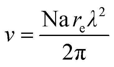 , with Na being the Avogadro number and re the classical electron radius (∼2.818 × 10⁻⁵ Å). Thus, as δ and β are dependent functions of the mass density of the material in a given layer, fitting both quantities independently may result in misinterpretation of the outputs due to the higher probability of calculating mass densities without physical meaning. Although a possible explanation for the deviations of the derived density compared to the literature would be the presence of crystallographic defects that may affect absorption, thus, β, independent fitting should be used with caution. One example of software that allows the user to fit δ and β independently is Parratt32.21 Even though Parratt32 is extremely powerful and fast, in order to obtain δ and β of the quantum heterostructures studied here, access to external databases is required. Another piece of software for the visualization and analysis of non-polarized specular reflectivity data is LEPTOS®.22 The software, developed by the Bruker company, does not require in advance knowledge of the SLD of a material and the mass density is the key parameter as in the case of MROX, an acronym for Multiple Reflection Optimization package for X-ray scattering. Although extremely versatile and powerful as it not only simulates experiments of X-ray reflectivity and diffraction but also grazing incidence small angle X-ray scattering (GISAXS), the commercial character of LEPTOS® reduces its attractivity. Several other types of software are available to simulate and fit XRR scans.23–29 MROX intends to stand out as a reliable, fast and highly versatile tool where layer creation and manipulation are extremely easy and the material database is readily accessible and editable. Furthermore, MROX provides a fast access list to the materials available in the database (DB). The fast access list and the DB are also editable. Therefore, the user may select materials according to specific interests or research fields. MROX is implemented in a modern design that guides the user through relevant suggestions (embedded text messages). Moreover, it enables the user to fit δ and β independently by requesting the user to quantify the SLD parameterization via an external file. Therefore, it transfers to the user the responsibility of employing SLD parameters instead of using the mass density per default. Preliminary versions of the MROX for X-ray reflectivity were developed in ref. 7, 8, 30 and 31. The final version, for the first time presented here, is made available to the scientific community on a dedicated website (https://www.mrox.eu). In section 2, the growth procedures of two sets of samples with increasing layering complexity are described. The first consists of 5 Si/Ge quantum heterostructures grown on Si buffer layers and (001) Si substrates. The second refers to a ZnO/ZnMgO superlattice containing 50 periods deposited on a ZnO buffer layer and m-ZnO substrate. The technological relevance of the layered structures studied here concerns their applicability to the optoelectronics field. In fact, concerning the cubic system, the reduction of the dimensionality from films to quantum wells/superlattices changes the density of states32,33 while the wurtzite system, as a wide band gap semiconductor, is suitable for a variety of applications, from near-UV emitters34 and sensors35 to laser structures as well.36 Furthermore, the experimental conditions used in the measurements of XRR scans are highlighted in section 2. The application of the MROX software in its reflectivity version to the different sets of samples is addressed in section 3, while in section 4, the main conclusions are summarized.
2. Samples and description of the experimental techniques
Two sets of samples are employed to demonstrate the applicability of the X-ray reflectivity package of the MROX software in the study of layered quantum heterostructures. The criteria for including the various samples in the manuscript are based upon the layering complexity and scientific area applicability of the different sets. The first set consists of an increasing number of 100 Å Si/∼10 Å Ge bilayers grown on ∼500 Å Si buffer layers and (001) Si substrates. The samples, grown by Molecular Beam Epitaxy (MBE), hereafter referred to as E1, E2, E3, E4 and E5, are schematically presented in Fig. 1a) and consist of stacks of 1, 2, 3, 4 and 10 Si/Ge periods, respectively. A detailed description of the growth procedure may be found in ref. 37. Succinctly, samples from the E series were grown using an electron beam evaporator for Si and an effusion cell with a crucible of pyrolytic BN for Ge and a base pressure lower than 10−10 mbar. A Si flux is tapered through Si films on (001) Si wafers with a growth rate of 1 Å per second. The growth of the Si/Ge heterostructures was performed at the Institute for Semiconductor Engineering, University of Stuttgart, Germany.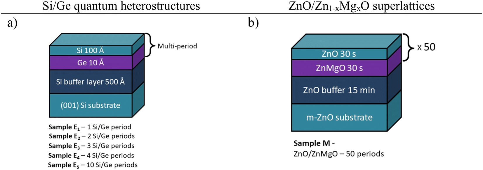 | ||
| Fig. 1 Schematic views of samples Ei {i = 1, 2, 3, 4, 5} with 100 Å Si/∼10 Å Ge bilayers grown on a Si buffer layer and (001) Si substrate a), and sample M with 50 periods of ZnO/Zn1−xMgxO layers grown on a ZnO buffer layer and m-ZnO substrate b). | ||
The sample for the second set (M) is a ZnO/Zn1−xMgxO superlattice grown on a commercial m-plane ZnO substrate by Plasma Assisted Molecular Beam Epitaxy (PA-MBE) using a Riber Compact 21 system. The term ‘superlattice’ is employed in the current work to describe sets of 2 layers with the same crystalline structure but different lattice parameters, thicknesses and roughnesses. In contrast to the previous set of samples, a detailed description of the growth procedure will follow as it is the first time that any kind of structural characterization is performed on the sample. Before the growth, the m-ZnO substrate was chemically cleaned in a (1![[thin space (1/6-em)]](https://www.rsc.org/images/entities/char_2009.gif) :1) H2SO4:H2O2 mixture for 5 min and then rinsed in deionized water and dried with nitrogen gas. Thermal purification of the substrate was carried out at a temperature of 150 °C for 1 h in the load chamber and then the substrate was transferred to the growth chamber where it was baked in a vacuum at 700 °C for 10 min. During the pre-growth process, the radio-frequency (RF) power of the oxygen plasma was fixed at 400 W, and the pure 6 N O2 gas flow rate was 3 sccm. The substrate was oxygenized in a plasma environment for about 3 minutes. After the preparation procedures, a ZnO buffer layer was deposited to separate the hydrothermally obtained substrate from the hydrogen-free SL structure. The ZnO buffer layer was grown for 15 minutes with a growth rate of about 30 Å min−1, with the oxygen flow reduced to 1.6 sccm. The buffer layer also was annealed, but in a vacuum at 600 °C for about 30 min. The SL structure, schematically presented in Fig. 1b), consists of 50 ZnO/Zn1−xMgxO bilayers. Pure Zn and Mg 7 N metals were evaporated from conventional two-zone Knudsen cells. The fluxes of Mg and Zn were measured before the growth with the beam flux monitor of a Bayard–Alpert type ionization gauge with a pressure of ∼4.04 × 10⁻⁸ torr and 1.3 × 10⁻⁶ torr for Mg and Zn, respectively. Furthermore, in sample M, Transmission Electron Microscopy (TEM) investigation and annular dark-field imaging (HAADF) were performed on the prepared transparent sediments for electron cross-sections of the ZnO/Zn1−xMgxO multilayer with the use of FEI Helios Nanolab 600 dual beam FEG-SEM/FIB apparatus equipped with an Omniprobe nano-manipulator and a platinum gas injection system (GIS). High Resolution Transmission Electron Microscopy (HRTEM) and Scanning Transmission Electron Microscopy (STEM) investigations were performed using an aberration-corrected FEI Titan cube 80–300 microscope operating at 300 kV and equipped with an energy-dispersive X-ray spectrometer (EDX). Prior to measurements, the structures were polished with a SiC abrasive with a gradual decrease in the size of the abrasive grain, followed by argon ion milling on a copper holder at room temperature. Images with a size of 2048–2048 pixels were registered using a CCD camera with a 2 s exposure time for a single acquisition. The surface roughness and morphology are obtained using Atomic Force Microscopy (AFM), allowing assessment of the flatness on the level of RMS = 0.81 nm. The growth of the oxide was performed at the Institute of Physics of the Polish Academy of Sciences, Warsaw, Poland.
:1) H2SO4:H2O2 mixture for 5 min and then rinsed in deionized water and dried with nitrogen gas. Thermal purification of the substrate was carried out at a temperature of 150 °C for 1 h in the load chamber and then the substrate was transferred to the growth chamber where it was baked in a vacuum at 700 °C for 10 min. During the pre-growth process, the radio-frequency (RF) power of the oxygen plasma was fixed at 400 W, and the pure 6 N O2 gas flow rate was 3 sccm. The substrate was oxygenized in a plasma environment for about 3 minutes. After the preparation procedures, a ZnO buffer layer was deposited to separate the hydrothermally obtained substrate from the hydrogen-free SL structure. The ZnO buffer layer was grown for 15 minutes with a growth rate of about 30 Å min−1, with the oxygen flow reduced to 1.6 sccm. The buffer layer also was annealed, but in a vacuum at 600 °C for about 30 min. The SL structure, schematically presented in Fig. 1b), consists of 50 ZnO/Zn1−xMgxO bilayers. Pure Zn and Mg 7 N metals were evaporated from conventional two-zone Knudsen cells. The fluxes of Mg and Zn were measured before the growth with the beam flux monitor of a Bayard–Alpert type ionization gauge with a pressure of ∼4.04 × 10⁻⁸ torr and 1.3 × 10⁻⁶ torr for Mg and Zn, respectively. Furthermore, in sample M, Transmission Electron Microscopy (TEM) investigation and annular dark-field imaging (HAADF) were performed on the prepared transparent sediments for electron cross-sections of the ZnO/Zn1−xMgxO multilayer with the use of FEI Helios Nanolab 600 dual beam FEG-SEM/FIB apparatus equipped with an Omniprobe nano-manipulator and a platinum gas injection system (GIS). High Resolution Transmission Electron Microscopy (HRTEM) and Scanning Transmission Electron Microscopy (STEM) investigations were performed using an aberration-corrected FEI Titan cube 80–300 microscope operating at 300 kV and equipped with an energy-dispersive X-ray spectrometer (EDX). Prior to measurements, the structures were polished with a SiC abrasive with a gradual decrease in the size of the abrasive grain, followed by argon ion milling on a copper holder at room temperature. Images with a size of 2048–2048 pixels were registered using a CCD camera with a 2 s exposure time for a single acquisition. The surface roughness and morphology are obtained using Atomic Force Microscopy (AFM), allowing assessment of the flatness on the level of RMS = 0.81 nm. The growth of the oxide was performed at the Institute of Physics of the Polish Academy of Sciences, Warsaw, Poland.
The X-ray reflectivity measurements were performed on a Bruker D8 AXS Series diffractometer equipped with a Göbel parabolic mirror to limit the vertical divergence and a 220 Ge monochromator to select the Cu Kα1 radiation (λ = 1.54056 Å). The component of the X-ray direct beam that travels parallel to the sample surface without experiencing reflection is blocked by a knife edge (KE) as shown in Fig. 2a). The reflected intensity is measured by a point focus detector after the beam is laterally limited by a Soller slit (S).
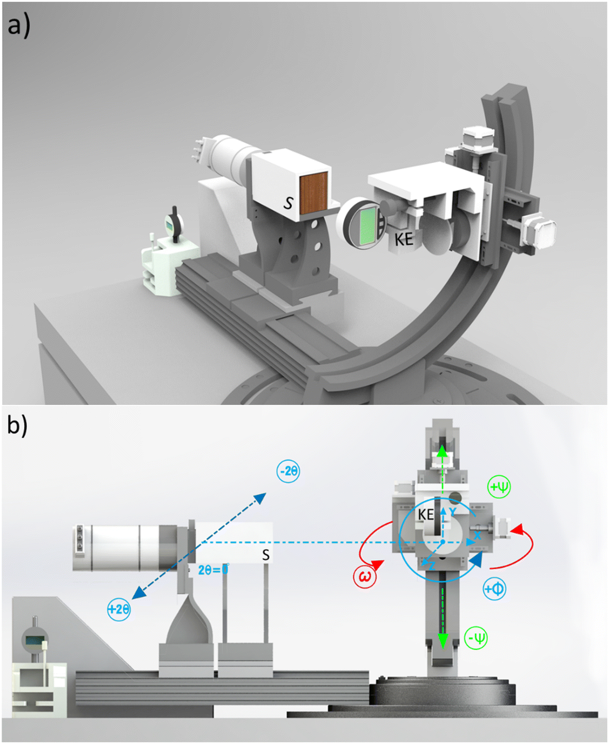 | ||
| Fig. 2 a) In the case of the X-ray reflectivity measurements, a Soller slit (S) is placed in front of the detector while to perform the high-resolution X-ray diffraction measurements, the Soller slit is replaced by a 0.1 mm width slit. The knife-edge (KE) with the function of blocking the direct beam not reflected at the surface is also shown. b) Goniometer showing the sample holder and detector schematics showing the possible scans to operate on the Bruker AXS D8 diffractometer. The sign convention used for the degrees of freedom at the measurement system is also shown. | ||
To align the typical θ–2θ scan that defines the XRR scan, first, the axes x, y, z, and ω depicted in Fig. 2b) were used to place the beam parallel to the sample surface, i.e., after centering the sample using the x- and y-axes, sets of z- and ω-scans are performed. Then, the detector axis (2θ) is moved to 0.2° and an ω-scan is accumulated. The maximum was defined in the acquisition software as half of the scattering angle (2θ/2). Due to the low roughness expected in high-quality single crystals, Yoneda wings were clearly observed, which facilitates the optimization process.15,19 In the present case, the maximum should be located at 0.1°. The same procedure is performed for 2θ = {0.15, 0.2, 0.25, 0.3}. As expected, the peak observed in the ω-scan shifts towards higher angles as 2θ increases with increasing ς off-set, (2θ/2) + ς. Therefore, a compromise of ω = 2θ/2 is chosen. The simulation and fit of the experimental data are successfully accomplished using the MROX extension for X-ray reflectivity. The simulations employ the recursive Parratt's formalism which is accounted under the frame of the dynamical theory of X-ray scattering.20,21 The software considers the instrumental function as the sum of a resolution function and a constant background. The resolution is determined by calculating the reflectivity averaged over several points, n, analytically defined by a Gaussian distribution and ranging from −a to a as 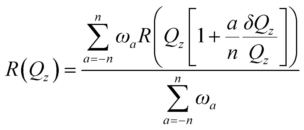 . δQz is the reciprocal space resolution and
 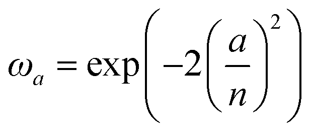 . The Genetic, Pattern Search and Simulated Annealing constitute the available fitting algorithms in MROX. A brief description of the theoretical background of the dynamical theory of X-ray specular reflectivity is addressed in S1 while in S2, the description of the MROX software is put forward ESI.†
3. Experimental results and MROX simulations
3.1 Si/Ge superlattices grown on Si buffer layers and (001) Si substrates – samples E1, E2, E3, E4 and E5
Fig. 3a) shows the MROX user interface highlighting the experimental (black colored dots) and simulated (blue colored line) X-ray reflectivity (XRR) scans of sample E2. The reasoning for showing sample E2 is based upon the fact that E2 is the first sample in the measured sequence to exhibit Kiessig fringes (KFs) and superlattice diffraction orders (SLs) simultaneously. The first eight identified KFs and SLs are presented.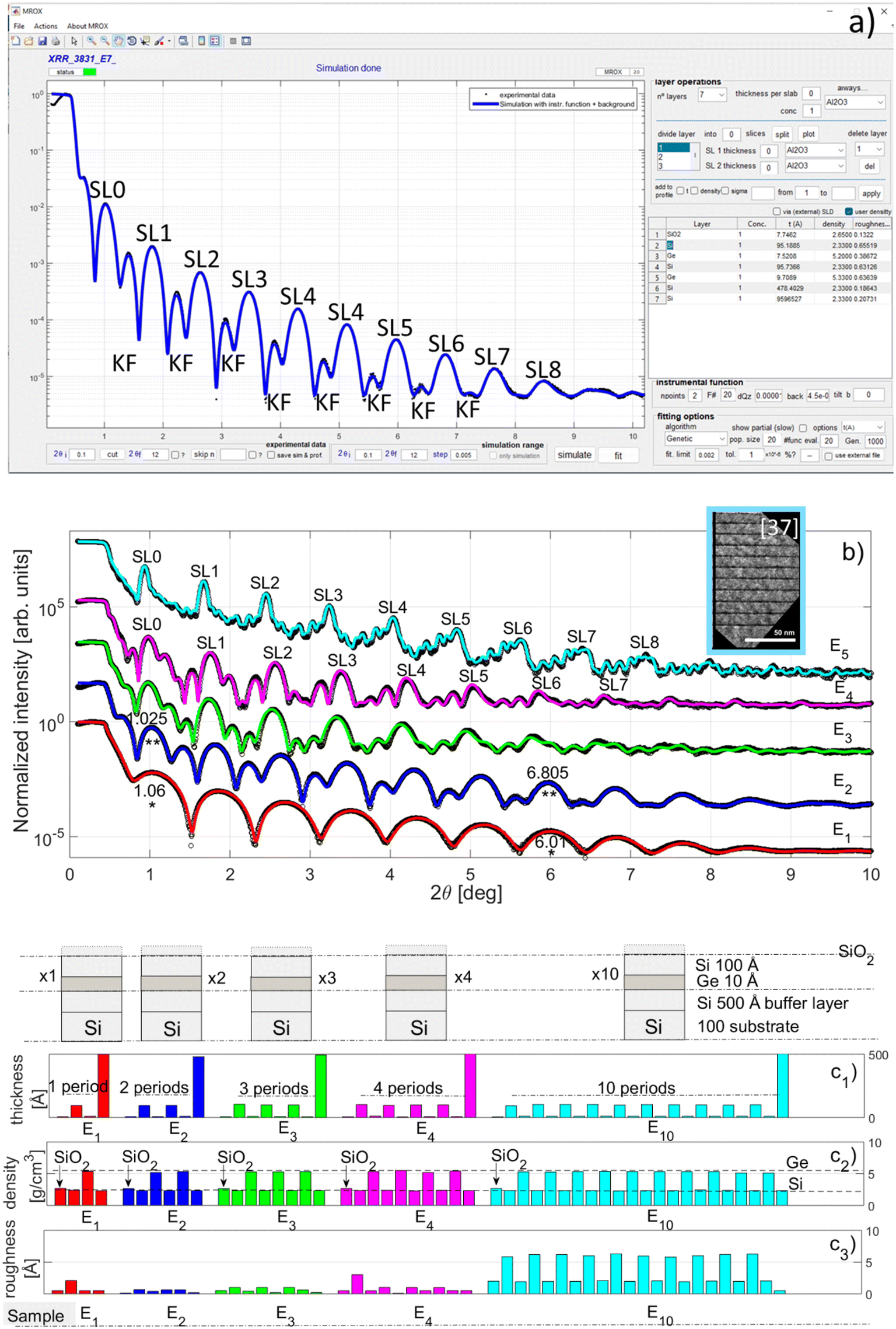 | ||
| Fig. 3 a) MROX graphical user interface showing the experimental (black colored dots) and simulation (blue curve) XRR scans of sample E2. b) Experimental (black colored dots) and simulated X-ray reflectivity scans of the 1 (E1), 2 (E2), 3 (E3), 4 (E4) and 10 (E5) Si/Ge periods grown on a Si buffer layer and (001) Si substrate. In the inset, a transmission electron microscopy image of the 10 period Si/Ge superlattice (sample E5) is shown.37 Bar graphs showing the depth-evolution of the thickness (in Å, c1), mass density (in g cm−3, c2) and roughness (in Å, c3) of the Si and Ge individual layers down to the Si buffer layer. For visualization purposes, the information regarding the Si substrate is discarded. | ||
The quality of the fit is very good with all the KFs and SLs accurately simulated. The high number of observed KFs and SLs is an indication of the high-quality interfaces.38 That is to say, the layer interfaces are sharp,39 and low levels of composition heterogeneities are expected. The derived thickness, mass density, and roughness of the 7 layers are the ones shown in Table 1 and the table embedded in the MROX user interface. Accordingly, the experimental data measured for sample E2 was simulated (and fitted) by including a thin SiO2 layer (∼7.7 Å), followed by 2 Si/Ge bilayers, i.e., 2 periods with corresponding layer thicknesses of 95.2 Å/7.5 Å and 95.7 Å/9.7 Å on top of a ∼478.4 Å Si buffer layer and a Si substrate. A thin oxidized Si or Ge surface layer is common in silicides and germanium-related compounds.40,41 The thicknesses of the individual periods are 102.7 Å (95.2 Å + 7.5 Å) and 105.4 Å (95.7 Å + 9.7 Å), suggesting the bilayer thickness homogeneity with just a slight dispersion of 2.7 Å.
| E2: layer | Thickness (Å) | Density (g cm−3) | Roughness (Å) |
|---|---|---|---|
| 1-SiO2 | 7.75 | 2.65 | 0.13 |
| 2-Si | 95.19 | 2.33 | 0.66 |
| 3-Ge | 7.52 | 5.20 | 0.39 |
| 4-Si | 95.74 | 2.33 | 0.63 |
| 5-Ge | 9.71 | 5.33 | 0.64 |
| 6-Si (buffer layer) | 478.40 | 2.33 | 0.19 |
| 7-Si (substrate) | — | 2.33 | 0.21 |
Furthermore, the XRR scan is also affected by the mass density of the materials that form the heterostructure. The mass density simulated for the surface layer is found to be 2.65 g cm−3 while the ones simulated for the Si and Ge layers are 2.33 g cm−3 (layers 2, 4, 6 and 7) and 5.2 g cm−3 and 5.33 g cm−3 (layers 3 and 5), respectively. The former matches with the theoretical value for a SiO2 compound42 while the latter two only differ by 0.1% and a maximum of 2% with respect to the Si and Ge theoretical densities, respectively.43,44 The above parameterization agrees with the respective nominal values indicated in Fig. 1a) and in ref. 37. A maximum difference of ∼21 Å is found for the Si buffer layer where a thickness of 500 Å would be expected. However, the effect of the thickness of the Si buffer layer in the reflectivity pattern is found to be negligible above 300 Å. The roughness is also deduced via simulations using the MROX software. According to the fitting outputs, the surface roughness is found to be 0.1 Å, highlighting its flat air/SiO2 interface. It is interesting to note that the thicker Si layers of the periodic structure reveal higher roughnesses compared to the thinner Ge layers. Specifically, the average roughness of layers 2 and 4 is ∼0.6339 Å (Si) while the same quantity is found to be around 20% lower for layers 3 and 5 (Ge), respectively. The roughnesses of the Si buffer layer and Si substrate are ∼0.19 Å and ∼0.21 Å, emphasizing the Si wafer quasi-flat surface prior to the growth of the bilayer quantum heterostructure. The derived roughnesses of the Si/Ge interfaces are close to the ones found in the literature for state-of-the-art Si/Ge superlattices.45–47 The experimental and simulated X-ray reflectivity scans of samples E1 to E5 are compared in Fig. 3b). The scans are vertically translated for clarity. For the case of sample E1, the quality of the fits is found to be very good while for the cases of samples E3, E4 and E5 slight deviations in the simulations compared to the respective experimental data are found. The deviations are suggested to be due to small composition heterogeneities where Si1−xGex compound thin layers could be stacked in-between the Si/Ge bilayers, and thus some interdiffusion is suggested. In fact, according to the literature, a low degree of interdiffusion is common in Si/Ge superlattices.48–50 The composition heterogeneities would change the mass density depth-distribution but the total thickness of a set of Si/Si1−xGex/Ge/Si1−xGex layers would be kept constant. The result is accurately simulated KFs, i.e., no simulated fringes would be out-of-phase with respect to the experimental ones because the total thickness is maintained, while affecting the KF and SL overall intensity. As evidenced, the increased number of Si/Ge periods is reflected in an increased number of SLs. In other words, the constructive interference adds-up as scattering events due to the number of Si/Ge bilayers increasing from sample E1 to E5. The image shown in the inset of Fig. 3b), obtained via transmission electron microscopy, highlights the 10 period Si/Ge superlattice (sample E5).37 From this image, it is not clear the interdiffusion suggested for the cases of samples with a higher number of periods. On the one hand, the XRR scan of sample E1 only shows the presence of oscillation fringes and no SLs are visible, which is a result of the scattering events due to the finite thickness of the individual layers. On the other hand, in the XRR scans of samples E2 to E5, the interference phenomena of the reflected X-ray waves arise not only from scattering events at the interfaces of the individual layers but also from the scattering events of the bilayer itself. Furthermore, the angular separation between KFs decreases from sample E1 to E5 evidencing the higher total thickness for samples with higher indices. Analytically, the thickness may be determined via the kinematical theory of X-ray scattering by employing the Bragg's law equivalent,  . Here, λ is the Cu Kα1 X-ray wavelength, and 2θj and 2θi are the maxima angular positions of KFs separated by n. In the case of sample E1 using 2θ/2 and the 1st and 7th KFs for the purpose of statistical improvement (n ⇒ 6 = 7 − 1), a thickness of 107.05 Å is calculated. Both KFs are marked in Fig. 3b) with a star symbol with the angular positions of 2θj = 6.01° and 2θi = 1.06°. For sample E2, the angular separation between SL7 (2θj = 6.805°) and SL1 (2θi = 1.025°) highlighted in Fig. 3b) with double star symbols results in ∼106.97 Å. Therefore, as expected, the angular separation between KFs is related to the thickness of the Si/Ge bilayer in sample E1, while in sample E2, the same quantity is measured by the angular separation between consecutive diffraction orders. As calculated from Table 1, the average Si/Ge heterostructure period is ∼104.08 Å which is slightly below (∼2.89 Å) the one found using the kinematical approximation. The individual layer thicknesses, mass densities and roughnesses of the layers of samples E1 to E5 are summarized in Fig. 3c1–3), respectively. It is interesting to note the increase in the overall roughness with an increasing number of periods being more accentuated for samples E4 and E5. The effect may be due to the increasing strain anticipated by the increasing number of bilayers leading to pseudomorphic growth of the superlattice which in turn degrades the morphology prior to layer relaxation. In fact, according to ref. 51 and 52, pseudomorphic growth may lead to a roughness increase in Si/Ge superlattices. Furthermore, in order to extract information about the crystallinity of the quantum heterostructure, the thicknesses derived via XRR were used as inputs in the X-ray diffraction (XRD) simulations. Although, in the range of a few nanometers, the sensitivity of XRR to the layer thickness is superior, it is interesting to point out that highly accurate XRD simulations were obtained. In fact, as the 2θ–ω scans around the 004 reciprocal lattice point measured for samples E1 to E5 evidence in Fig. 4a), the match between both techniques is almost perfect. The 2θ–ω scans were vertically translated for clarity. The MROX code, as recognized software for the simulation of X-ray diffraction measurements, was used in X-ray diffraction single reflection mode.53–58 The simulations considered pseudomorphic growth, i.e., the Ge in-plane lattice parameter equals the ones from the Si substrate and Si buffer layer. Although the measured reflection is only sensitive in the orthogonal direction with respect to the surface, as it is only dependent on the c-lattice parameter, the calculated intensity is slightly affected by the volume of the unit cell which is different if the unit cell is relaxed or strained uniaxially.59 In fact, previous XRD reciprocal space maps around an asymmetric reflection show that Ge is not relaxed but fully strained instead.37 Furthermore, the derived strain perpendicular to the sample surface (ε⊥) presented in Fig. 4b) suggests higher strain in the Si SL layers than on the Ge ones while the Si buffer is found to be almost relaxed in the direction perpendicular to the sample surface and fully relaxed in the orthogonal direction. The crystalline quality was simulated as a Debye–Waller parameter (DW).60 The evolution of the DW as a function of depth for the five samples suggests lower crystalline quality for samples with higher indices/periods which may be related to the higher roughnesses derived via XRR. To summarize the section, the simulations of the XRD results fully agree with the XRR conclusions and a combined reflectivity/diffraction approach presents advantages over the single scattering mode of the respective configurations.
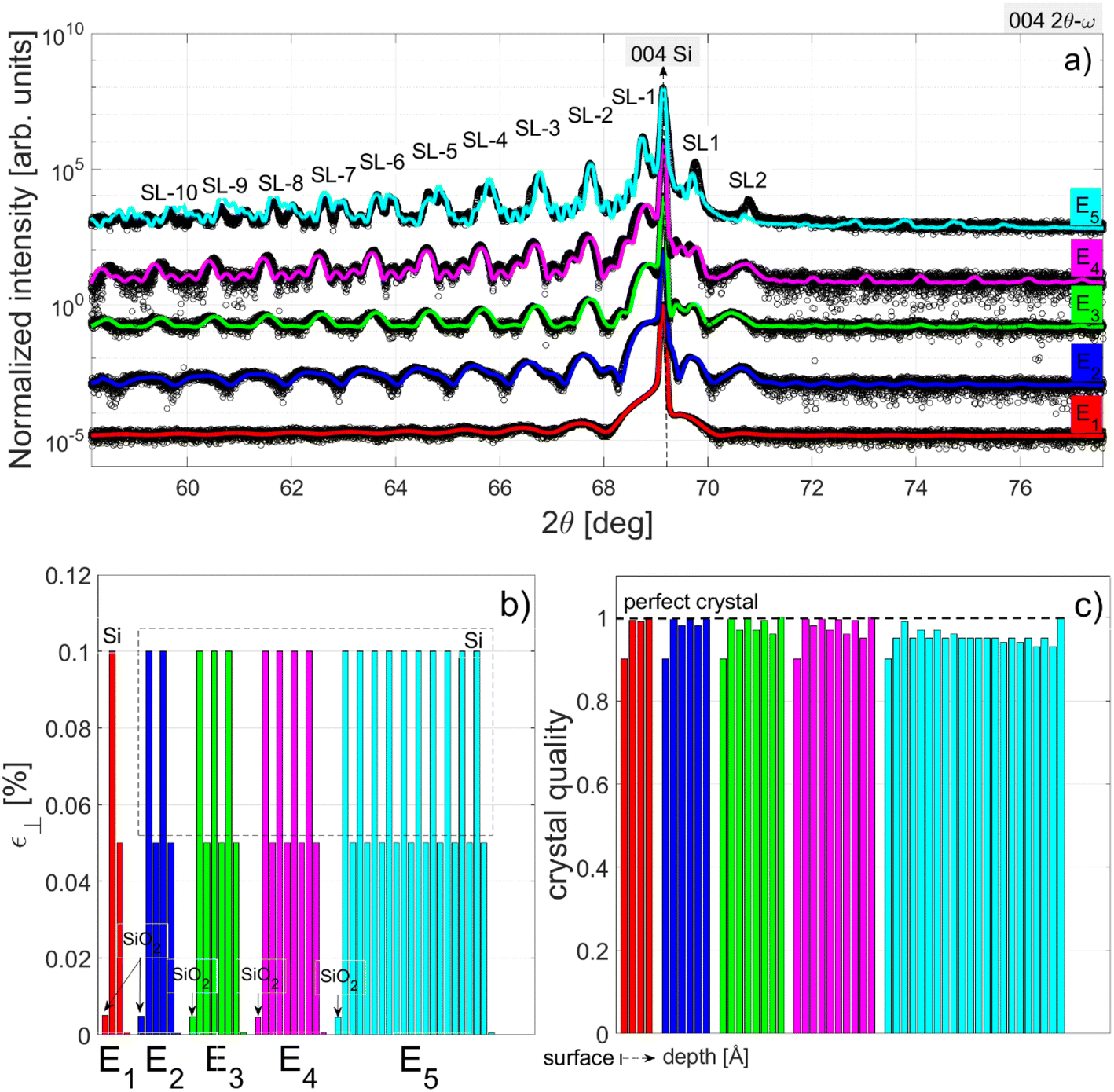 | ||
| Fig. 4 a) Experimental (black colored dots) and simulated X-ray 2θ–ω scans around the 004 Si reciprocal lattice point of the E1, E2, E3, E4, and E5 samples. The individual scans were vertically translated for clarity. Strain perpendicular to the sample surface b), and Debye–Waller parameter (crystalline quality) c) depth-profiles derived for samples E1 to E5. | ||
3.2 ZnO/Zn1−xMgxO bilayers grown on ZnO buffer layers and m-ZnO substrates
The application of MROX to the XRR measurements of a sample containing 50 periods of ZnO/Zn1−xMgxO bilayers grown on a ZnO buffer layer and m-ZnO substrate is discussed as follows. As is evidenced in the TEM/STEM images depicted in Fig. 5a) and b), significant changes in the roughness are found if observed along the a-axis (<11![[2 with combining macron]](https://www.rsc.org/images/entities/char_0032_0304.gif) 0>, Fig. 5a1–2) or along the c-axis (<0001>, Fig. 5b). In fact, the interface layer roughness is more pronounced or less sharp when probed along the a-axis rather than along the c-axis.
0>, Fig. 5a1–2) or along the c-axis (<0001>, Fig. 5b). In fact, the interface layer roughness is more pronounced or less sharp when probed along the a-axis rather than along the c-axis.
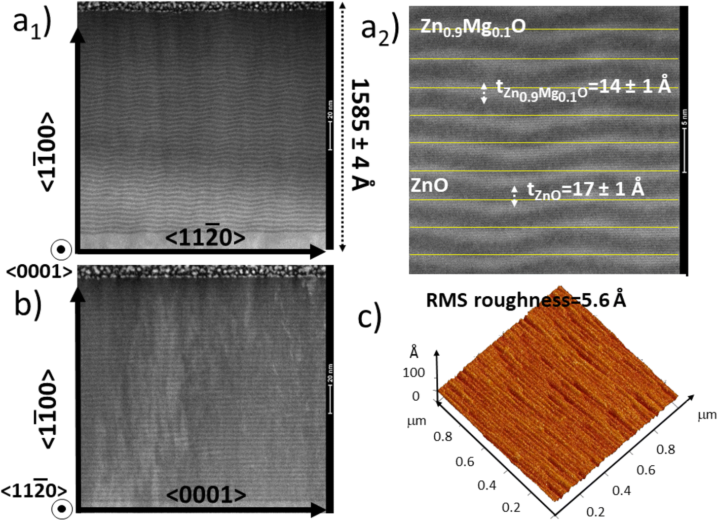 | ||
Fig. 5 a) TEM a1) and STEM a2) images acquired along the <110> axis highlighting the entire superlattice and a random 9-period depth-region in the superlattice, respectively. From the STEM analysis, the thickness of the ZnO and Zn1−xMgxO layers is found to be 17 ± 1 Å and 14 ± 1 Å, respectively. The average total thickness of the superlattice is 1585 ± 4 Å. The interface roughness modulation is evidenced by the deviations in the material's mass density with respect to the horizontal yellow lines. b) TEM image measured along the <0001> axis showing the full structure of the quantum heterostructure. In a) and b), the vertical direction corresponds to the growth direction, <1![[1 with combining macron]](https://www.rsc.org/images/entities/char_0031_0304.gif) 00>. All layers are parallel to the substrate surface. c) AFM image evidencing elongated stripes along the c-axis. The RMS roughness is found to be 5.6 Å. 00>. All layers are parallel to the substrate surface. c) AFM image evidencing elongated stripes along the c-axis. The RMS roughness is found to be 5.6 Å. | ||
Fig. 5a2) shows a magnification of the TEM image illustrated in Fig. 5a1). The magnification corresponds to a 9-period region from Fig. 5a1). The horizontal yellow lines evidence the roughness modulation along the a-axis. The roughness amplitude is similar amongst all the interfaces. Specifically, the roughness amplitude is around half of the thickness of the layer, while the number of oscillations per unit of area decreases towards the surface. Moreover, by comparing Fig. 5a1) and b), the morphology of the ZnO buffer layer is suggested to be the driving force for the wavy character of the interfaces of the overall structure. In fact, according to the literature, replication of the buffer layer roughness towards the surface is common in several superlattice systems such as Si/Ge,61 GaAs/AlAs,62 and GaN/AlN.63,64 The high level of alignment between the atoms in both ZnO and Zn1−xMgxO layers as well as the individual layer thicknesses is concluded from the high-resolution STEM image of Fig. 5a2). The total thickness of the superlattice is 1585 ± 14 Å while the average thicknesses and respective standard deviations considering the 50 ZnO and Zn1−xMgxO layers are found to be 17 ± 1 Å and 14 ± 1 Å, respectively. A root mean square (RMS) surface roughness of 5.6 Å is measured through AFM. Furthermore, the AFM image depicted in Fig. 5c) shows elongated stripes along the c-axis, in agreement with that observed in ref. 65 by Chauveau et al. Along the red and light blue lines in Fig. 6a1–2) corresponding to the STEM a- and the c-axes observations, respectively, the hill to bottom amplitudes amount to 3 Å thick in average (not shown). The regions crossed by both lines are chemically characterized by a random Zn1−xMgxO compound with the MgO content varying between pure ZnO and maximum MgO content available in the layers. Since the sample was not annealed after growing, the high variations in the MgO contents depicted in Fig. 6b1–2) are suggested to be due to strain-induced spontaneous intermixing.66,67
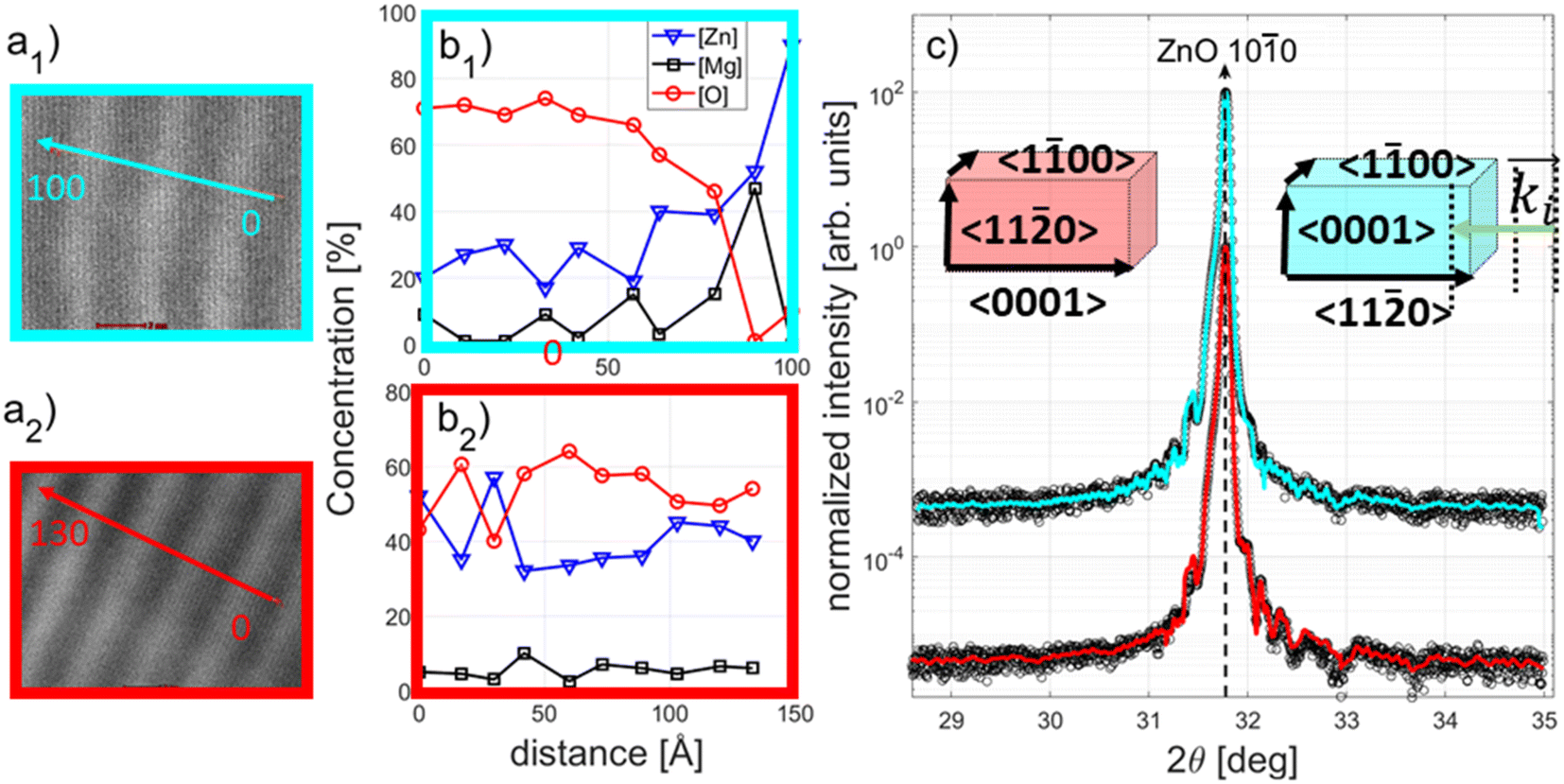 | ||
| Fig. 6 STEM observation along the <110> a1) and <0001> a2) axes of a randomly selected depth-region of the quantum heterostructure. Concentrations of Zn, Mg and O b1) and b2) determined along the light blue and red arrows shown in a1) and a2), respectively. The lengths of the arrows are 100 Å and 130 Å, respectively. c) Experimental and simulated 2θ–ω scans around the 100 ZnO reciprocal lattice point. | ||
The intriguing observation of the different interface roughnesses along the a- and c-axes observed via STEM/TEM motivated the XRD/XRR measurements as direct comparison with visual techniques is possible. Concretely, the thickness of the individual layers and the chemical composition may be deduced via the simulations of the XRD and XRR scans while the roughness is accessible through the simulations of the latter. Therefore, as in the case of the Si/Ge heterostructures, XRD and XRR measurements of the ZnO/Zn1−xMgxO bilayer superlattice were performed and simulated using the MROX code in the reflectivity and diffraction single reflection modes, respectively. Fig. 6c) shows the experimental and simulated 2θ–ω scans around the 100 ZnO reciprocal lattice point for the sample with the a- and c-axes perpendicular to the incident wavevector ((![[k with combining right harpoon above (vector)]](https://www.rsc.org/images/entities/i_char_006b_20d1.gif) i), respectively. As in the case of the STEM images in Fig. 6a1–2) and the concentration of Zn, Mg and O plotted as a function of distance in Fig. 6b1–2), the 2θ–ω scan with the a-axis perpendicular to the X-ray beam is presented in light blue while the latter scan is shown in red. The latter measurement with the respective simulation is translated vertically for clarity. The 100 ZnO Bragg peak from the substrate and buffer layer is clearly identified while, at first glance, no SLs or KFs are visible. As the ZnO/Zn1−xMgxO bilayer thickness is 31 Å, the total thickness of the superlattice is expected to be around 1500 Å (31 Å × 50 periods or 1585 Å determined via STEM). Converting both thicknesses into angular spacings, consecutive SLs/KFs would be separated by 2.8°/0.056°, respectively. Because the particular diffraction and interference signatures expected in a quantum heterostructure are not present in the measurements, simulations of the 2θ–ω scans are required for accurate structural characterization. The simulations depicted in Fig. 6c) were performed considering the averaged thickness determined via STEM for ZnO and Zn1−xMgxO, i.e., 17 Å and 14 Å, respectively, while, in order to include the microscopy observations shown in Fig. 6a1–2) and b1–2), random in-depth MgO contents varying between 2% and 15% were considered. Furthermore, random variations of the strain along the growth direction were added, in agreement with the Geometric Phase Analysis determined via STEM (not shown). The dynamical theory model considered here does not account for the effects of the roughness in the diffraction patterns. Instead, a Debye–Waller parameter ranging between 1 and 0 is included to model the structure factor of the individual layers ranging from a perfect to a highly distorted crystal. The best fits were accomplished with DWs of 0.7 and 1 in the cases of the X-ray beam being perpendicular to the a-/c-axis, respectively. Therefore, the crystalline quality interpreted as a decrease in the crystalline structure factor caused by a decrease in the DW factor is expected to be lower for the case when the X-ray beam is perpendicular to the a-axis. The thicknesses of the individual and buffer layers perfectly agree with the ones observed via STEM. The thicknesses derived via XRD were used as inputs for the simulations of the XRR scans. Fig. 7a) shows the experimental and simulated XRR scans acquired for different azimuth angles: ϕ = {0°, 20°, 40°, 60°, 80°, 90°} (check Fig. 1b) for the definition of the azimuth angle). The former corresponds to the X-ray beam perpendicular to the c-axis while the latter measurement relates to the X-ray beam perpendicular to the a-axis. All the simulations agree perfectly with the experimental data. The mass density of the Zn1−xMgxO layers was included in the XRR simulations assuming a linear interpolation between the mass densities of ZnO (5.61 g cm−3)68 and MgO (3.58 g cm−3)69 weighed by the MgO content derived via XRD. The averaged MgO content calculated over all the ZnMgO layers anticipates small differences in the refractive indexes of consecutive layers, thus, on the density of the ZnO and Zn0.9Mg0.1O. The contrast in the refractive index of consecutive layers is barely noticeable due to the absence of KFs in the XRR scans while 3 SLs are identified in Fig. 7 as SL0, SL1 and SL2. As described in the previous section, the distance between consecutive SLs is related to the superlattice period. Using SL0 (2θ = 2.92032°) and SL2 (2θ = 8.56798°), a period of 31.3 Å is found which perfectly agrees with the bilayer thickness input in the simulations. The roughness in individual layers is also determined via XRR simulations. Values between 1 Å and 8 Å were employed for each layer but with an average of 1.9916 Å, 2.8357 Å, 2.9897 Å, 4.8101 Å, 5.5272 Å, and 5.9101 Å for measurements performed with increasing azimuth angle as depicted in Fig. 7a) and b). The averaged roughness considering the total number of layers increases from ϕ = 0° to ϕ = 90°. Furthermore, the surface layer roughness increases with increasing azimuth angle as presented in Fig. 7b). Therefore, the simulation of the XRR scans suggests an overall roughness dependency on the azimuth angle which agrees with the high-resolution TEM results.
i), respectively. As in the case of the STEM images in Fig. 6a1–2) and the concentration of Zn, Mg and O plotted as a function of distance in Fig. 6b1–2), the 2θ–ω scan with the a-axis perpendicular to the X-ray beam is presented in light blue while the latter scan is shown in red. The latter measurement with the respective simulation is translated vertically for clarity. The 100 ZnO Bragg peak from the substrate and buffer layer is clearly identified while, at first glance, no SLs or KFs are visible. As the ZnO/Zn1−xMgxO bilayer thickness is 31 Å, the total thickness of the superlattice is expected to be around 1500 Å (31 Å × 50 periods or 1585 Å determined via STEM). Converting both thicknesses into angular spacings, consecutive SLs/KFs would be separated by 2.8°/0.056°, respectively. Because the particular diffraction and interference signatures expected in a quantum heterostructure are not present in the measurements, simulations of the 2θ–ω scans are required for accurate structural characterization. The simulations depicted in Fig. 6c) were performed considering the averaged thickness determined via STEM for ZnO and Zn1−xMgxO, i.e., 17 Å and 14 Å, respectively, while, in order to include the microscopy observations shown in Fig. 6a1–2) and b1–2), random in-depth MgO contents varying between 2% and 15% were considered. Furthermore, random variations of the strain along the growth direction were added, in agreement with the Geometric Phase Analysis determined via STEM (not shown). The dynamical theory model considered here does not account for the effects of the roughness in the diffraction patterns. Instead, a Debye–Waller parameter ranging between 1 and 0 is included to model the structure factor of the individual layers ranging from a perfect to a highly distorted crystal. The best fits were accomplished with DWs of 0.7 and 1 in the cases of the X-ray beam being perpendicular to the a-/c-axis, respectively. Therefore, the crystalline quality interpreted as a decrease in the crystalline structure factor caused by a decrease in the DW factor is expected to be lower for the case when the X-ray beam is perpendicular to the a-axis. The thicknesses of the individual and buffer layers perfectly agree with the ones observed via STEM. The thicknesses derived via XRD were used as inputs for the simulations of the XRR scans. Fig. 7a) shows the experimental and simulated XRR scans acquired for different azimuth angles: ϕ = {0°, 20°, 40°, 60°, 80°, 90°} (check Fig. 1b) for the definition of the azimuth angle). The former corresponds to the X-ray beam perpendicular to the c-axis while the latter measurement relates to the X-ray beam perpendicular to the a-axis. All the simulations agree perfectly with the experimental data. The mass density of the Zn1−xMgxO layers was included in the XRR simulations assuming a linear interpolation between the mass densities of ZnO (5.61 g cm−3)68 and MgO (3.58 g cm−3)69 weighed by the MgO content derived via XRD. The averaged MgO content calculated over all the ZnMgO layers anticipates small differences in the refractive indexes of consecutive layers, thus, on the density of the ZnO and Zn0.9Mg0.1O. The contrast in the refractive index of consecutive layers is barely noticeable due to the absence of KFs in the XRR scans while 3 SLs are identified in Fig. 7 as SL0, SL1 and SL2. As described in the previous section, the distance between consecutive SLs is related to the superlattice period. Using SL0 (2θ = 2.92032°) and SL2 (2θ = 8.56798°), a period of 31.3 Å is found which perfectly agrees with the bilayer thickness input in the simulations. The roughness in individual layers is also determined via XRR simulations. Values between 1 Å and 8 Å were employed for each layer but with an average of 1.9916 Å, 2.8357 Å, 2.9897 Å, 4.8101 Å, 5.5272 Å, and 5.9101 Å for measurements performed with increasing azimuth angle as depicted in Fig. 7a) and b). The averaged roughness considering the total number of layers increases from ϕ = 0° to ϕ = 90°. Furthermore, the surface layer roughness increases with increasing azimuth angle as presented in Fig. 7b). Therefore, the simulation of the XRR scans suggests an overall roughness dependency on the azimuth angle which agrees with the high-resolution TEM results.
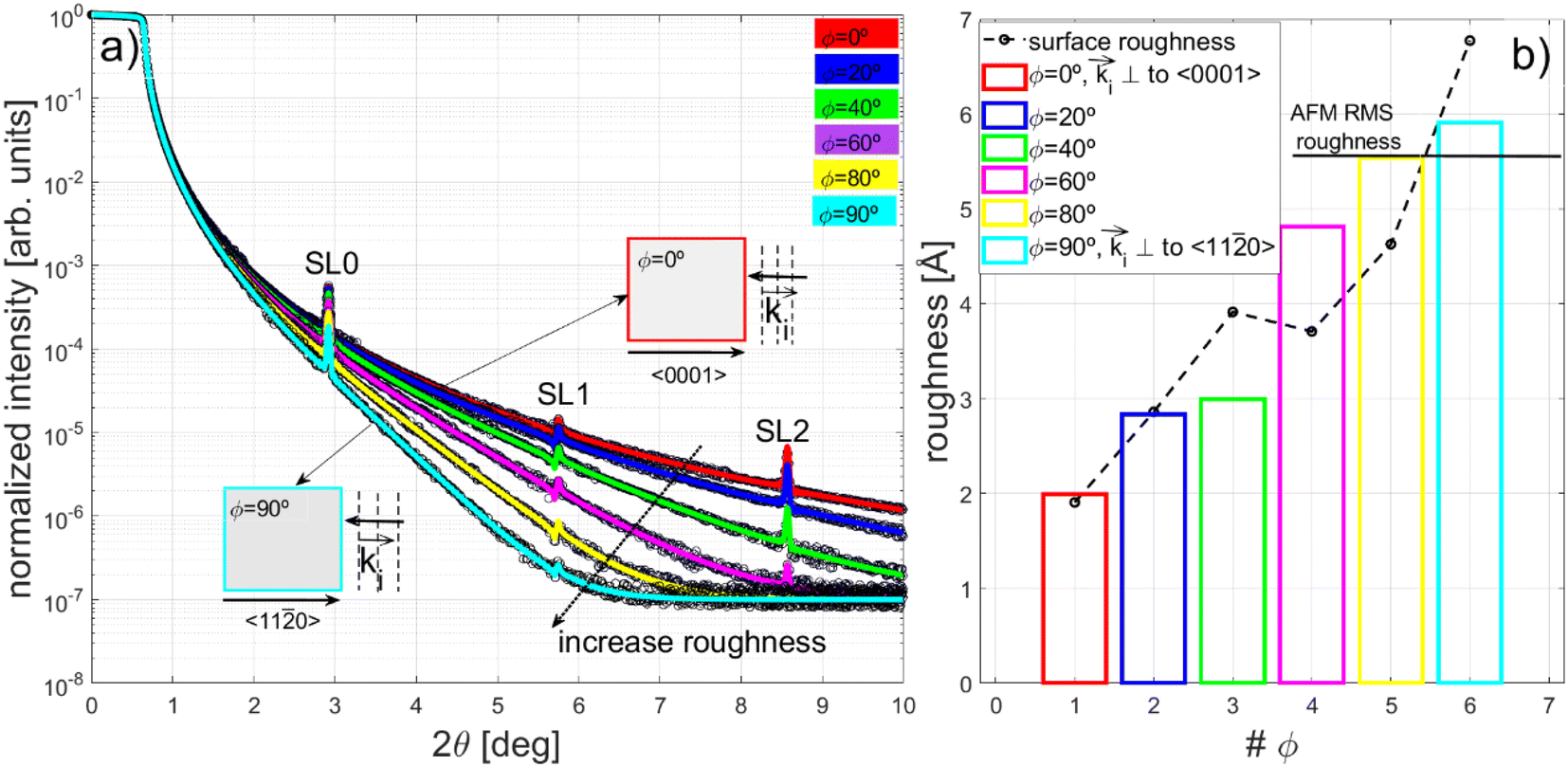 | ||
| Fig. 7 a) Experimental and simulated XRR scans for different azimuth angles: ϕ = {0°, 20°, 40°, 60°, 80°, 90°}. b) Average of the roughnesses between all layers of the quantum heterostructure (bars) and the surface layer roughness as a function of the azimuth ϕ angle (black dashed line). | ||
4. Conclusions
In the present work, an extension of the Multiple Reflection Optimization package for X-ray diffraction focusing on the simulation and fitting of non-polarized specular X-ray reflectivity (XRR) measurements is developed. The recursive Parratt's formalism of the dynamical theory of X-ray scattering is employed to determine the layer thicknesses, mass densities and roughnesses of quantum heterostructures of two sets of heterostructures samples. The first set consists of 5 samples of Si/Ge bilayer superlattices with 1, 2, 3, 4 and 10 periods grown on Si buffer layers and on (001) Si substrates followed by a 50 period ZnO/Zn1−xMgxO bilayer grown on a ZnO buffer layer on a m-ZnO substrate. In order to consider typical surface oxidation in Si capping layers, a thin SiO2 layer was included at the surface in the simulations of the reflectivity patterns of the group IV elemental semiconductors with the novel MROX code. The thicknesses agree with the ones expected by the growth procedure and by direct imaging visual techniques. Moreover, the thicknesses derived via the simulations of the XRR scans were used as inputs in the MROX simulations of the radial 004 2θ–ω scans. Perfect agreement is found for the cases of a low number of periods while for higher numbers, interdiffusion and/or roughness effects may play an important role and are not considered in the case of X-ray diffraction. The derived mass densities of Si, SiO2 and Ge agree with the ones found in the literature. Furthermore, the simulations of the XRR scans allows quantifying higher roughness in samples characterized by a higher number of periods, in particular, in the case of the 4 and 10 sets of Si/Ge bilayers. The higher roughness is suggested to be related to the decrease of the crystalline quality based on the Debye–Waller parameter derived via XRD simulations. With respect to the second set concerning the zinc oxide related superlattices, XRR and XRD measurements were simulated. The low incidence reflectivity measurements were motivated by high-resolution transmission electron microscopy observations (HR-TEM), where the roughness was found to be dependent on the sample azimuth orientation. Consequently, XRR scans were accumulated for different azimuth angles (ϕ) of 0°, 20°, 40°, 60°, 80° and 90°. In the former azimuth angle, the X-ray beam is put parallel to the a-axis, while in the latter, the X-ray beam is parallel to the c-axis. With perfect agreement with HR-TEM, the XRR simulations reveal lower roughnesses for ϕ = 0°. Furthermore, the derived thickness of the individual layers forming the complex superlattice and Zn1−xMgxO used for capping and buffering agree perfectly with the ones directly determined via TEM. The low Mg incorporation in the Zn1−xMgxO compound of xMg ∼ 0.1 induces low contrast in the refractive index of the bilayer constituents and is manifested in the very low intensity of superlattice diffraction orders in the XRR scans. The single presence of Kiessig fringes is not enough to accurately determine the density of the compound. For this reason, the chemical composition was determined via simulations of the XRD 100 2θ–ω scans considering the linear interpolation between the ZnO and MgO binaries (Vegard's rule). Then, the mass density was extrapolated via a weighted average between the mass densities of the binaries. Combining X-ray reflectivity and diffraction measurements constitutes, thus, a fundamental asset while analyzing the structural properties of quantum heterostructures.Conflicts of interest
There are no conflicts to declare.Acknowledgements
This work was supported by the Portuguese Foundation for Science and Technology (FCT) in the framework of the Plurianual Strategic Funding UID/FIS/50010/2019. FO acknowledges the FCT PhD Grant and thanks the Institut für Halbleitertechnik, Universität Stuttgart for its hospitality.References
- M. Yasaka, X-ray thin-film measurement techniques V. X-ray reflectivity measurement, Rigaku J., 2010, 6(2), 01–09 Search PubMed , ISSN 2187 9974.
- N. Samsudin, M. F. Omar and N. S. Rudin, X-Ray Reflectivity Analysis in Evaluating Multilayer Thin Film Fabrication, Key Eng. Mater., 2022, 908, 537–542, DOI:10.4028/p-z5v069.
- B. Bierska-Piech, D. Chocyk, A. Proszynski and E. Łągiewka, The Characteristic of the Multilayer Thin Films by X-Ray Reflectometry Method, Solid State Phenom., 2010, 163, 80–83, DOI:10.4028/www.scientific.net/SSP.163.80.
- R. A. Cowley and T. W. Ryan, J. Phys. D: Appl. Phys., 1986, 20, 61 CrossRef.
- E. Chason and T. M. Mayer, Thin film and surface characterization by specular X-ray reflectivity, Crit. Rev. Solid State Mater. Sci., 1997, 22(1), 1–67, DOI:10.1080/10408439708241258.
- V. Holý, U. Pietsch and T. Baumbach, High-Resolution X-Ray Scattering from Thin Films and Multilayers, Springer, 1999, vol. 174 Search PubMed.
- S. Magalhães, M. Fonseca, N. Franco, N. Barradas, N. Sobolev, R. Hey, H. Grahn and E. Alves, Damage behaviour of GaAs/AlAs multilayer structures, Nuclear Instruments & Methods in Physics Research Section B-beam Interactions With Materials and Atoms, Nucl. Instrum. Methods Phys. Res., Sect. B, 2006, 249, 890–893, DOI:10.1016/j.nimb.2006.03.157.
- P. Jozwik, S. Magalhães, R. Ratajczak, C. Mieszczynski, M. Sequeira, A. Turos, R. Böttger, R. Heller, K. Lorenz and E. Alves, RBS/C, XRR, and XRD Studies of Damage Buildup in Er-Implanted ZnO, Phys. Status Solidi B, 2018, 256, 1800364, DOI:10.1002/pssb.201800364.
- P. Persans, A. Ruppert, V. Pantojas, K. Liang, G. Hughes and B. Abeles, Interface Roughness and X-Ray Reflectivity of Amorphous Semiconductor Multilayers, MRS Online Proc. Libr., 1990, 192, 225–230, DOI:10.1557/PROC-192-225.
- M. Lué-Merú and E. Hernández-Caraballo, Direct Analysis of Biological Samples by Total Reflection X-Ray Fluorescence, Spectrochim. Acta, Part B, 2004, 36, 1077–1090, DOI:10.1016/j.sab.2004.05.017.
- C. E. Miller, J. Majewski, T. Gog and T. L. Kuhl, Characterization of biological thin films at the solid-liquid interface by x-ray reflectivity, Phys. Rev. Lett., 2005, 94(23), 238104, DOI:10.1103/PhysRevLett.94.238104 , Epub 2005 Jun 16, PMID: 16090507.
- C. Reich, D. Photonen, M. Hochrein, B. Krause and B. Nickel, A Microfluidic Setup for Studies of Solid-Liquid Interfaces using X-ray Reflectivity and Fluorescence Microscopy, Rev. Sci. Instrum., 2005, 76, 095103, DOI:10.1063/1.2040187.
- J. Tiilikainen, M. Bosund, M. Mattila, T. Huhtio, J. Sormunen and H. Lipsanen, Fitness function and nonunique solutions in x-ray reflectivity curve fitting: Crosserror between surface roughness and mass density, J. Phys. D: Appl. Phys., 2007, 40, 4259, DOI:10.1088/0022-3727/40/14/023.
- Y. Fujii, Comparison of Surface Roughness Estimations by X-ray Reflectivity Measurements and TEM observations, IOP Conf. Ser.: Mater. Sci. Eng., 2011, 24, 012008, DOI:10.1088/1757-899x/24/1/012008.
- L. G. Parratt, Surface Studies of Solids by Total Reflection of X-Rays, Phys. Rev., 1954, 95(2), 359–369, DOI:10.1103/physrev.95.359.
- S. K. Sinha, E. B. Sirota, S. Garoff and H. B. Stanley, X-ray and neutron scattering from rough surfaces, Phys. Rev. B, 1988, 38(4), 2297–2311, DOI:10.1103/physrevb.38.2297.
- H. Kiessig, Untersuchungen zur Total reflexion von Röntgenstrahlen, Ann. Phys., 1931, 402(6), 715–768, DOI:10.1002/andp.19314020607.
- V. Holý, J. Kuběna, I. Ohlídal, K. Lischka and W. Plotz, X-ray reflection from rough layered systems, Phys. Rev. B, 1993, 47(23), 15896–15903, DOI:10.1103/PhysRevB.47.15896.
- P. Mikulík, X-ray reflectivity from planar and structured multilayers, PhD thesis, University of Joseph Fourier, Grenoble, France, 1997 Search PubMed.
- K. Stoev and K. Sakurai, Recent theoretical models in grazing incidence x-ray reflectometry, Rigaku J., 1997, 14, 22 CAS.
- D. Kumar, M. Gupta, D. Kumar, A. K. Singh and A. Kumar, Deposition of Fe/Nb multilayers and Fe/Nb/Fe trilayers using HIPIMS: XRR measurements for interface diffusion study, AIP Conf. Proc., 2019, 2142, 080006, DOI:10.1063/1.5122434.
- A. Ulyanenkov, Novel methods and universal software for HRXRD, XRR and GISAXS data interpretation, Appl. Surf. Sci., 2006, 253, 106–111, DOI:10.1016/j.apsusc.2006.05.099.
- N. Andrew, Motofit – Integrating neutron reflectometry acquisition, reduction and analysis into one, easy to use, package, J. Phys.: Conf. Ser., 2010, 251, 012094, DOI:10.1088/1742-6596/251/1/012094.
- G. Fragneto, F. Graner, T. Charitat, P. Dubos and E. Bellet-Amalric, Interaction of the Third Helix of Antennapedia Homeodomain with a Deposited Phospholipid Bilayer: A Neutron Reflectivity Structural Study, Langmuir, 2000, 16(10), 4581–4588, DOI:10.1021/la991119s.
- K. H. Stone, S. M. Valvidares and J. B. Kortright, Kramers-Kronig constrained modeling of soft x-ray reflectivity spectra: Obtaining depth resolution of electronic and chemical structure, Phys. Rev. B, 2012, 86, 024102, DOI:10.1103/PhysRevB.86.024102.
- P. A. Kienzle, M. Doucet, D. J. McGillivray, K. V. O'Donovan, N. F. Berk and C. F. Majkrzak, https://www.ncnr.nist.gov/reflpak, pp. 2000–2006.
- C. H. Russell and M. C. Polson, Limitations in critical angle determination with grazing incidence x-ray reflectivity, Proc. SPIE 5918, Laser-Generated, Synchrotron, and Other Laboratory X-Ray and EUV Sources, Optics, and Applications II, 31 August 2005, p. 591808, DOI:10.1117/12.625157.
- B. P. Toperverg and H. Zabel, Neutron Scattering in Nanomagnetism, in Experimental Methods in the Physical Sciences, ed. F. Fernandez-Alonso and D. L. Price, Academic Press, 2015, ch. 6, vol. 48, pp. 339–434, ISSN 1079–4042, ISBN 9780128020494, DOI:10.1016/B978-0-12-802049-4.00006-3.
- J. F. Ankner and G. P. Felcher, Polarized-neutron reflectometry, J. Magn. Magn. Mater., 1999, 200, 741–754 CrossRef CAS.
- B. M. S. Teixeira, A. A. Timopheev, N. Caçoilo, L. Cuchet, J. Mondaud, J. R. Childress, S. Magalhães, E. Alves and N. A. Sobolev, Ar+ ion irradiation of magnetic tunnel junction multilayers: impact on the magnetic and electrical properties, J. Phys. D: Appl. Phys., 2020, 53(45), 455003, DOI:10.1088/1361-6463/aba38c.
- A. Marciel, M. Graça, A. Bastos, L. Pereira, K. J. Suresh, J. Borges, F. Vaz, M. Peres, S. Magalhães, K. Lorenz and R. Silva, Molybdenum Oxide Thin Films Grown on Flexible ITO-Coated PET Substrates, Materials, 2021, 14(4), 821, DOI:10.3390/ma14040821.
- K. L. Wang, D. Cha, J. Liu and C. Chen, Proc. IEEE, 2007, 95, 1866, DOI:10.1109/JPROC.2007.900971.
- E. Onaran, M. C. Onbasli, A. Yesilyurt, H. Y. Yu, A. M. Nayfeh and A. K. Okyay, Opt. Express, 2012, 20, 7608 CrossRef CAS PubMed.
- J.-M. Chauveau, D. A. Buell, M. Laügt, P. Vennéguès, M. Teisseire-Doninelli, S. B. Bergery, C. Deparis, B. Lo, B. Vinter and C. Morhain, Growth of non-polar ZnO/(Zn, Mg)O quantum well structures on R-sapphire by plasma-assisted molecular beam epitaxy, J. Cryst. Growth, 2007, 301–302, 366–369, DOI:10.1016/j.jcrysgro.2006.11.320.
- D. J. Rogers, F. H. Teherani, A. Yasan, K. Minder, P. Kung and M. Razeghi, Electroluminescence at 375 nm from a Zno/GaN:Mg/c-Al2O3 heterojunction light emitting diode, Appl. Phys. Lett., 2006, 88, 141918, DOI:10.1063/1.2195009.
- K. Liu, M. Sakurai and M. Aono, ZnO-Based Ultraviolet Photodetectors, Sensors, 2010, 10, 8604–8634, DOI:10.3390/s100908604.
- F. Oliveira, I. A. Fischer, A Benedetti, M. F. Cerqueira, M. I. Vasilevskiy, S. Stefanov, S. Chiussi and J. Schulze, Multi-stacks of epitaxial GeSn self-assembled dots in Si: structural analysis, J. Appl. Phys., 2015, 117, 125706 CrossRef.
- V. Holy, J. Kubena, I. Ohlidal, K. Lischka and W. Plotz, Phys. Rev. B, 1993, 47, 15896, DOI:10.1103/PhysRevB.47.15896.
- Y. Yoneda, Phys. Rev., 1963, 131, 2010, DOI:10.1103/PhysRev.131.2010.
- N. Ozguven and P. C. Mcintyre, Oxidation-enhanced interdiffusion in Si1−xGex/Si1−yGey superlattices, Appl. Phys. Lett., 2008, 90, 082109, DOI:10.1063/1.2434162.
- S. M. Prokes, O. J. Glembocki, S. K. Brierley, J. M. Gibson and J. M. Woodall, Control of semiconductor surfaces and interfaces, Mater. Res. Soc. Symp. Proc., 1996, 448 Search PubMed , https://apps.dtic.mil/sti/pdfs/ADA328464.pdf.
- S. Y. Zhang, et al., Mechanical, elastic and thermal properties of SiO2: A molecular dynamics study, Comput. Mater. Sci., 2009, 47, 249–256 CrossRef.
- I. Henins, Precision density measurement of Silicon, J. Res. Natl. Bur. Stand. A Phys. Chem., 1964, 68A(5), 529–533, DOI:10.6028/jres.068A.050.
- T. B. Light, Density for “Amorphous” Ge, Phys. Rev. Lett., 1969, 22, 999, DOI:10.1103/PhysRevLett.22.999.
- P. Schaaf, et al., X-ray scattering and transmission electron microscopy characterization of Ge/Si(001) superlattices grown by molecular beam epitaxy, Thin Solid Films, 2000, 361–362, 312–317 Search PubMed.
- R. L. Headrick and J. Baribeau, Correlated roughness in (Gem/Sin)p superlattices on Si(100), Phys. Rev. B: Condens. Matter, 1993, 48(12), 9174–9177, DOI:10.1103/physrevb.48.9174 , PMID: 10007149.
- A. R. Powell, D. K. Bowen, M. Wormington, R. A. Kubiak, E. H. C. Parker, J. Hudson and P. D. Augustus, X-ray diffraction and reflectivity characterization of SiGe superlattice structures, Semicond. Sci. Technol., 1992, 7, 627, DOI:10.1088/0268-1242/7/5/001.
- I. A. Papadogonas, A. Andriotis and E. Economou, Dependence of the energy and form of the optical-absorption onset of interface diffusion in SinGem superlattices, Phys. Rev. B, 1997, 55, R4887, DOI:10.1103/PhysRevB.55.R4887.
- S. J. Chang, V. Arbet and K. L. Wang, et al, Studies of interdiffusion in GemSin strained layer superlattices, J. Electron. Mater., 1990, 19, 125–129, DOI:10.1007/BF02651736.
- Y. Dong, A systematic study of silicon germanium interdiffusion for next generation semiconductor devices (T), Doctor of Philosophy in The Faculty of Graduate and Postdoctoral Studies (Materials Engineering), University of British Columbia, 2014 Search PubMed.
- H. Ye and J. Yu, Germanium epitaxy on silicon, Sci. Technol. Adv. Mater., 2014, 15, 024601, DOI:10.1088/1468-6996/15/2/024601.
- S. Mukherjee, A. Attiaoui, M. Bauer and O. Moutanabbir, 3D Atomic Mapping of Interfacial Roughness and Its Spatial Correlation Length in Sub-10 nm Superlattices, ACS Appl. Mater. Interfaces, 2020, 12(1), 1728–1736, DOI:10.1021/acsami.9b13802 , Epub 2019 Dec 20, PMID: 31808669.
- S. Magalhães, J. S. Cabaço, J. P. Araújo and E. Alves, Multiple Reflection optimization package for X-ray diffraction, CrystEngComm, 2021, 23, 3308–3318 RSC.
- J. S. Cabaço, D. Nd. Faye, J. P. Araújo, E. Alves and S. Magalhães, Simulating the effect of Ar+ energy implantation on the strain propagation in AlGaN, J. Phys. D: Appl. Phys., 2021, 54, 245301 CrossRef.
- S. Magalhães, J. S. Cabaço, R. Mateus, D. Nd. Faye, D. R. Pereira, M. Peres and K. Lorenz, Crystal mosaicity determined by a novel layer deconvolution Williamson–Hall method, CrystEngComm, 2021, 23(10), 2048–2062 RSC.
- P. Mendes, K. Lorenz, E. Alves, S. Schwaiger, F. Scholz and S. Magalhães, Measuring strain caused by ion implantation in GaN, Mater. Sci. Semicond. Process., 2019, 98, 95–99 CrossRef CAS.
- S. Magalhães, M. Fialho, M. Peres, K. Lorenz and E. Alves, Quantitative x-ray diffraction analysis of bimodal damage distributions in Tm implanted Al0.15Ga0.85N, J. Phys. D: Appl. Phys., 2016, 49, 13 CrossRef.
- M. Fialho, S. Magalhães, M. P. Chauvat, P. Ruterana, K. Lorenz and E. Alves, Impact of implantation geometry and fluence on structural properties of AlxGa1-xN implanted with thulium, J. Appl. Phys., 2016, 120, 16 CrossRef.
- W. J. Bartels, J. Hornstra and D. J. W. Lobeek, X-ray diffraction of Multilayers and Superlattices, Acta Crystallogr., Sect. A: Found. Crystallogr., 1986, 42, 539–545, DOI:10.1107/S0108767386098768.
- N. Sousbie, L. Capello, J. Eymery, F. Rieutord and C. Lagahe, X-ray scattering study of hydrogen implantation in silicon, J. Appl. Phys., 2006, 99, 103509, DOI:10.1063/1.2198928.
- R. L. Headrick and J. M. Baribeau, Interface roughness in Ge/Si superlattices, J. Vac. Sci. Technol., B: Microelectron. Nanometer Struct.--Process., Meas., Phenom., 1993, 11, 1514, DOI:10.1116/1.586961.
- N. V. Nguyen, J. C. Pellegrino, P. M. Amirtharaj and D. G. Seiler, Interface roughness of short-perioid GaAs/AlAs superlattices studied by spectroscopic ellipsometry, J. Appl. Phys., 1993, 73, 7739, DOI:10.1063/1.353972.
- U. Choi, D. Jung, K. Lee, T. Kwak, T. Jang, Y. Nam, B. So and O. Nam, The effect of AlN buffer layer on AlGaN/GaN/AlN double heterostructure high-electron mobility transistor, Phys. Status Solidi A, 2020, 217(7), 1900694 CrossRef CAS.
- S. Magalhães, K. Lorenz, N. Franco, N. P. Barradas, E. Alves, T. Monteiro, B. Amstatt, V. Fellmann and B. Daudin, Effect of annealing on GaN/AlN quantum dot heterostructures: advanced ion beam characterization and X-ray study of low-dimensional structures, Surf. Interface Anal., 2010, 42(10–11), 1552–1555, DOI:10.1002/sia.3614.
- N. L. Biavan, M. Hugues, M. M. Bajo, J. T-Arriola, A. Jollivet, D. Lefebvre, Y. Cordier, B. Vinter, F.-H. Julien, A. Hierro and J.-M. Chauveau, Homoepitaxy of non-polar ZnO/(Zn,Mg)O multi-quantum wells: from a precise growth control to the observation of intersubband transitions, Appl. Phys. Lett., 2017, 111, 231903, DOI:10.1063/1.5003146.
- J. A. Davis, L. V. Dao, X. Wen, C. Ticknor, P. Hannaford, V. A. Coleman, H. H. Tan, C. Jagadish, K. Koike, S. Sasa, M. Inoue and M. Yano, Suppression of the internal electric field effects in ZnO/Zn0.7Mg0.3O quantum wells by ion-implantation induced intermixing, Nanotechnology, 2008, 19, 055205, DOI:10.1088/0957-4484/19/05/055205.
- V. A. Coleman, M. Buda, H. H. Tan, C. Jagadish, M. R. Phillips, K. Koike, S. Sasa, M. Inoue and M. Yano, Observation of blue shifts in ZnO/ZnMgO multiple quantum well structures by ion-implantation induced intermixing, Semicond. Sci. Technol., 2006, 21, L25–L28, DOI:10.1088/0268-1242/21/3/L02.
- C. D. Hodgman, M. F. Coolbaugh and C. E. Senseman, A ready reference pocket book of chemical and physical data, Cleveland, Handbook of Chemistry and Physics, CRC Press (formerly The Chemical Rubber Company), Ohio, USA, 101st edn, 1920, ISBN 9780367417246 Search PubMed.
- W. M. Haynes, CRC Handbook of Chemistry and Physics, CRC Press, Boca Raton, FL, 92nd edn, 2011, pp. 4–74, ISBN 1-4398-5511-0 Search PubMed.
Footnote |
| † Electronic supplementary information (ESI) available. See DOI: https://doi.org/10.1039/d3ce00371j |
| This journal is © The Royal Society of Chemistry 2023 |