DOI:
10.1039/D2CE01278B
(Paper)
CrystEngComm, 2023,
25, 95-107
Effect of rare-earth (RE) ionic radius on the dielectric properties of Sr99%RE1%TiO3 (RE = La, Nd, Yb) single crystals†
Received
15th September 2022
, Accepted 22nd November 2022
First published on 25th November 2022
Abstract
High-performance dielectric materials are essential components of electronic devices. In this work, RE-doped SrTiO3 (RE = La, Nd, Yb) single crystals with excellent dielectric properties were prepared by the Verneuil method. For La-STO and Nd-STO, the RE ions are substituted for Sr2+ only, and the excellent dielectric properties are mainly caused by defect dipoles associated with oxygen vacancies including 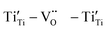 and
and 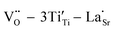 defect dipole clusters. For Yb-STO, Yb3+ partially replaces Ti4+, forming an additional defect dipole
  , resulting in the best dielectric properties (ε′ = 3.6 × 10⁴, tan
![[thin space (1/6-em)]](https://www.rsc.org/images/entities/char_2009.gif) δ = 0.0036 under 1 kHz). In addition, N2 atmosphere treatment promotes the production of oxygen vacancies and Ti3+ and the formation of more defect dipoles, thus further optimizing the dielectric properties of Yb-STO (ε′ = 4.9 × 10⁴, tanδ = 0.004 under 1 kHz). This work suggests that the dielectric properties of RE-doped SrTiO3 materials are closely related to oxygen vacancies, and the simultaneous substitution of Sr2+ and Ti4+ should enable obtaining dielectric properties superior to those of the substitution of Sr2+ only. The present work provides a clearer understanding of the origin of SrTiO3 dielectric properties, which is of great significance to the development of SrTiO3-based dielectric materials.
δ = 0.0036 under 1 kHz). In addition, N2 atmosphere treatment promotes the production of oxygen vacancies and Ti3+ and the formation of more defect dipoles, thus further optimizing the dielectric properties of Yb-STO (ε′ = 4.9 × 10⁴, tanδ = 0.004 under 1 kHz). This work suggests that the dielectric properties of RE-doped SrTiO3 materials are closely related to oxygen vacancies, and the simultaneous substitution of Sr2+ and Ti4+ should enable obtaining dielectric properties superior to those of the substitution of Sr2+ only. The present work provides a clearer understanding of the origin of SrTiO3 dielectric properties, which is of great significance to the development of SrTiO3-based dielectric materials.
1. Introduction
With the rapid development of information technology, especially in the electronics and microelectronics industries, higher requirements are put forward for the performance of dielectric materials.1,2 How to obtain materials with high dielectric constant, low dielectric loss, good temperature and frequency stability has become an important research direction of dielectric materials.3 Many dielectric materials with colossal permittivity (CP) have been studied, including CaCu3Ti4O12 (CCTO),4 A2/3Cu3Ti4O12 (A = trivalent rare earth or Bi),5–7 doped-BaTiO3,8–10 doped NiO,11,12 doped TiO213–16 and doped SrTiO3.17–19 However, there are still some specific problems with these materials that limit their practical application. For example, doped BaTiO3 shows a strong temperature-dependent behavior of the dielectric response,20 while CCTO and NiO are limited in capacitor applications due to high dielectric loss.21,22
In addition, the exact mechanism and explanation of CP generation are still unclear, which makes it impossible to have a good control of the dielectric properties of materials. Initially, it was thought that a new intrinsic polarization mechanism caused by charge order and/or crystal structure might be related to CP performance.23,24 Subsequently, a large number of studies have shown that a well-known extrinsic excitation of Maxwell–Wagner (MW) polarization, which is associated with inhomogeneous electrical properties between grains and grain boundaries, can produce CP in some cases.25–27 More recently, a model of electron-pinned defect dipoles (EPDDs) was proposed in Nb + In co-doped TiO2 ceramic material.28–30 According to the EPDD theory, several modified TiO2 materials do have higher dielectric constant and lower dielectric loss than materials in other systems.23,25,28–30 It is well known that the EPDD mechanism is also used in other materials and that the choice of the matrix material has an important influence on the dielectric properties. In addition, defect chemical design has always been an effective method to improve material properties, and an appropriate defect concentration often leads to excellent dielectric properties.
SrTiO3 (STO) is a favourable dielectric material with low dielectric loss (<0.01). Moreover, STO has better structure stability and dielectric stability than TiO2.31 In the past decades, a number of isovalent ion substitutions in STO ceramics, such as Sr2+ in the A-site replaced by Ba2+, Ca2+ or Pb2+, and Ti4+ in the B-site replaced by Zr4+, have been widely studied and reported as having preferable enhanced dielectric properties.32–36 In addition, rare earth oxide (Pr2O3, Gd2O3, La2O3, Nd2O3, Y2O3, Ce2O3, Sm2O3) doped STO ceramics have attracted the extensive attention of researchers in recent years due to their unique dielectric properties.37–43 Although the dielectric properties have been significantly improved, their origin remains unclear. The Maxwell–Wagner polarization initiates the CP behavior of Y-modified STO ceramics.39 Sm-doped STO ceramics sintered in N2 atmosphere obtained colossal permittivity and low dielectric loss, interpreted as a result of the production of the electron-pinned defect dipoles.40 The EPDD effect leads to the improvement of the dielectric properties of Nd-doped STO ceramics.42 Sr vacancies and Ti vacancies are considered to be the origin of the CP properties of La-doped STO ceramics.43 The main factors resulting in CP behavior are defect dipoles that come in contact with O vacancies for Ho-doped STO ceramics.44 Previous studies have mostly focused on STO ceramics, which contain defects such as grain boundaries and porosity, so their dielectric properties are particularly sensitive to the preparation process, and there are few studies on STO single crystals, especially STO single crystals doped with rare earth elements of different sizes. The influence of doping rare earth atoms on dielectric properties is not well understood due to the existence of inhomogeneous microstructures such as grain boundaries and pores in ceramics. To better explore the origin of dielectric properties of STO materials and the effect of rare earth element doping, it is increasingly significant to study the dielectric properties of rare earth-doped STO single crystals. In addition, fewer defects in crystals result in lower dielectric loss.45
In this work, Sr99%RE1%TiO3 (RE = La, Nd, Yb) single crystals were prepared by the Verneuil method and their dielectric properties were studied. Doping with different sizes of rare earth elements can produce different types of defects, resulting in different dielectric properties. Understanding the relationship between the sizes of the doped rare earth elements and the dielectric properties, while excluding the interference of grain boundaries and porosity, is important for the development and design of STO-based CP materials.
2. Experimental
Previously, we have prepared LaxSr1−xTiO3 (x = 1%, 3%, 5%, 8%) single crystals by the Verneuil method. It was found that when the doping amount reached 8%, it was difficult to obtain a stable solid–liquid interface. When the doping amount was 5%, although crystal growth could be achieved, serious crystal cracking occurred. When the doping amount was 3%, slight cracking was found. Thus, in the present experiment, a doping amount of 1% was chosen. SrTiO3 and Sr99%RE1%TiO3 (RE = La, Nd, Yb) powder was prepared by the traditional solid-state method using rutile TiO2 (Aladdin, 99.99%), SrCO3 (Aladdin, 99.99%), Nd2O3 (Aladdin, 99.99%), Yb2O3 (Aladdin, 99.99%) and La2O3 (Aladdin, 99.99%) as the starting materials. Subsequently, crystals with different compositions were grown by the Verneuil method. The schematic diagram of the device is shown in Fig. 1a. The crystal growth was carried out by using a two-channel burner, in which the central hole is O2 and the outer ring is H2. A 3 mm × 3 mm × 10 mm crystal column with the (200) crystal face as the growth plane was used as seed crystal. The crystal was grown at a rate of 14 mm h−1. The process is shown in Fig. 1b. First, the furnace was ignited using the parameters H2 16 L min−1 and O2 6.4 L min−1. After the chamber was preheated, a seed crystal was placed and gradually raised to the observation hole position. Second, the O2 flow rate was gradually increased until the top of the seed crystal melted, then the feeding system and crystal dropping device were turned on. Third, the powder melt fell on the seed crystal, and when a clear solid–liquid interface appeared, the H2 and O2 flow rates were increased simultaneously and the crystal started to expand its shoulder. Fourth, after the crystal grew to the desired size, the H2 and O2 flow rates were kept constant to maintain the crystal isometric growth. Finally, when the crystal grew to the ideal length, the gas valve and feeding system were closed, and the furnace was insulated to prevent cracking of the crystal caused by rapid cooling. During the whole process, the feed rate and crystal drop rate need to be controlled to keep the crystal dropping slowly, and the horizontal position of the crystals needs to be adjusted at all times to maintain a stable solid–liquid interface (see Fig. S1†). The grown crystals were annealed for a long time in a muffle furnace to eliminate the thermal stress formed during growth, and the specific annealing process is shown in Fig. S2.† The annealed crystals were cut into 10 mm × 10 mm × 2 mm slices using a diamond wire (STX-202A) after orientation determination. The cut wafers were defined as STO, La-STO, Nd-STO and Yb-STO. Subsequently, Yb-STO was annealed under N2 atmosphere at 1400 °C for 4 h, and it was recorded as N2-Yb-STO.
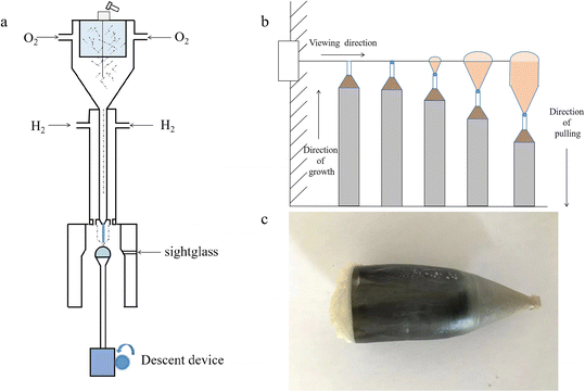 |
| | Fig. 1 (a) Schematic diagram of the equipment. (b) Diagram of the growth process. (c) STO crystal after long annealing. | |
The phase composition and crystal structure were examined by X-ray diffraction (XRD, Rigaku SmartLab, CuKα) and Raman spectroscopy (Horiba Jobin Yvon). The co-doped crystals were observed by scanning electron microscopy (SEM, Ultra Plus, ZEISS) combined with EDS after thermal etching at 1300 °C for 2 h. Transmission electron microscopy (TEM, JEOL JEM-2100F TEM) was used to characterize the detailed microstructure of the sample. X-ray photoelectron spectroscopy (XPS, Shimadzu Kratos Analytical, UK) was adopted to detect the valence states of elements. A layer of Ag was coated on the specimens by screen printing and sintered at 700 °C for 10 minutes. The dielectric behaviors and the impedance spectra at room temperature and high temperatures were measured using an electrochemical impedance spectrometer (TH 2839) equipped with a heating device.
3. Results and discussion
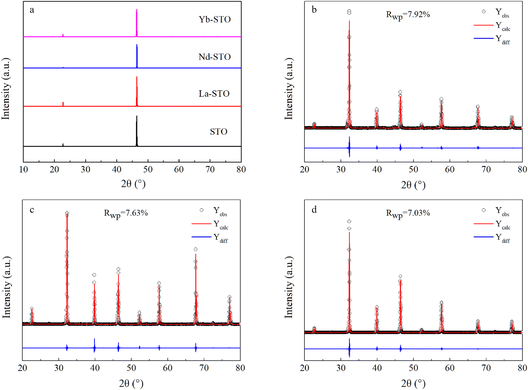
The annealed doped crystals are all similar to that shown in Fig. 1c. Even after a long time of annealing, the crystals remain black, indicating that they still contain oxygen vacancies and Ti3+. Fig. S3a† shows the XRD pattern of SrTiO3 and Sr99%RE1%TiO3 (RE = La, Nd, Yb) powders synthesized by the solid phase method. All samples show the pure perovskite structure and no secondary impurity phases can be detected, indicating that the RE elements have successfully entered the perovskite lattice. Fig. S3b† presents a detailed view of the (110) diffraction peak. It can be seen that the change in peak position is easily observed relative to pure STO. The (110) diffraction peak shifts to a larger angle with the addition of La3+ and Nd3+ ions because the ionic radii of La3+ (1.36 Å, C.N. = 12)46 and Nd3+ (1.27 Å, C.N. = 12)47 are smaller than that of Sr2+(1.44 Å, C.N. = 12),48 demonstrating that La3+ and Nd3+ have substituted for Sr2+ ions. In contrast, the smallest Yb3+ ions instead make the (110) diffraction peak shift to a lower angle. This indicates that the substitution of Yb3+ for Ti4+ occurs in Yb-STO. This phenomenon has been previously reported49,50 due to the fact that the ionic radius of Yb3+ (0.868 Å) is smaller than that of Sr2+ (1.44 Å) but larger than that of Ti4+ (0.605 Å) and closer to Ti4+.
Fig. 2a shows the XRD patterns of SrTiO3 and Sr99%RE1%TiO3 (RE = La, Nd, Yb) single crystals. They all maintain a (200) crystal orientation, which proves that we successfully obtained high-quality crystals. In order to obtain the crystal lattice constants, the block crystals were ground into powder, and the XRD patterns of the powder were tested. Fig. 2b and c show the Rietveld refinement results for La-STO and Nd-STO with pure STO cubic structure. The lattice parameters calculated from Rietveld refinement profile fits are 3.902 Å and 3.898 Å, respectively, slightly lower than the standard value of STO (3.904 Å) (ICSD-94573). The decrease of the lattice size could be attributed to the smaller ionic radii of La3+ and Nd3+ that occupy the position of Sr2+. Fig. 2d shows the Rietveld refinement result of Yb-STO, and its lattice constant was calculated to be 3.907 Å, which again confirms that some of the Yb3+ replace Ti4+, resulting in a larger lattice constant.
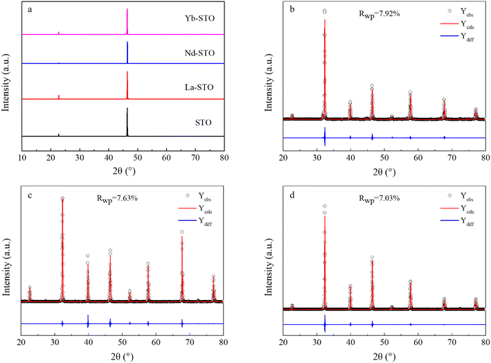 |
| | Fig. 2 (a) XRD patterns of STO crystals. (b)–(d) Rietveld refinement results for Sr99%RE1%TiO3 (RE = La, Nd, Yb) single crystals, respectively. | |
Fig. S4† shows the SEM images of Sr99%RE1%TiO3 (RE = La, Nd, Yb) single crystals. All the samples show a smooth surface, and energy-dispersive X-ray spectroscopy shows that the elements are evenly distributed and there is no element segregation, indicating that we have obtained high-quality crystals, thus excluding the influence of grain boundaries, pores and second-phase structures on subsequent dielectric properties. In order to better determine the integrity of the crystals, high-resolution images of Nd-STO under TEM were observed as an example. Fig. S5† shows the HRTEM images of the Nd-STO single crystals, indicating that the crystals are relatively perfect. Selected area electron diffraction (SAED) patterns also confirm the good crystallinity of the Nd-STO single crystal. The EDS elemental distribution maps of the low-magnification TEM images indicate that the composition of the Nd-STO crystals is homogeneous.
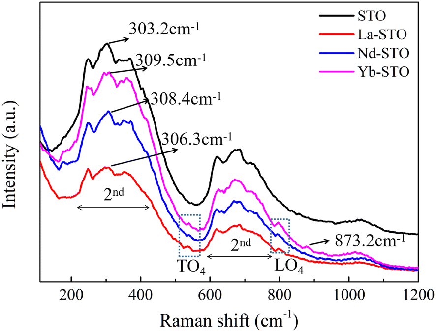
Raman spectroscopy is an effective method to study the local structure symmetry and chemical bond changes of materials. As shown in Fig. 3, the Raman spectra of crystals before and after doping show the same trend, indicating that they belong to the same crystal space group.51 SrTiO3 crystals with ideal cubic structure will not generate first-order Raman modes at room temperature, but due to the existence of defects, the symmetry is relaxed and these prohibited first-order scattering modes will be activated. In our case, all samples have two strong scattering bands in the range of 220–400 cm−1 and 600–750 cm−1, which is a classical cubic second-order Raman mode,52 and the Raman peak at about 300 cm−1 is an in-plane vibrational mode of the oxygen sublattice (B1 mode).53 Compared with the Raman peak of the SrTiO3 crystal (303.2 cm−1), the Raman peaks of the La, Nd, and Yb doped crystals are shifted to 309.5 cm−1, 308.4 cm−1 and 306.3 cm−1, respectively. The change in Raman peak position is related to the non-centrosymmetric Jahn–Teller distortion due to the accumulation of oxygen ions.54,55 Larger shifts correspond to larger distortion, and it can be seen that Yb doping causes the largest distortion. In addition, two weak scattering peaks of the doped crystal near 538 cm−1 and 793 cm−1 can be assigned to the TO4 mode and LO4 mode, respectively, which are caused by surface oxygen vacancies or higher polarity defects.56 Moreover, a weak scattering peak (873.2 cm−1) sensitive to the B site is observed in Yb-STO, indicating that the Ti4+ ion shares the B site with Yb3+ and causes a change in the Ti–O structure, confirming that Yb3+ may replace some Ti4+.57
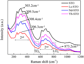 |
| | Fig. 3 Room-temperature Raman spectra of the STO single crystals with different doping. | |
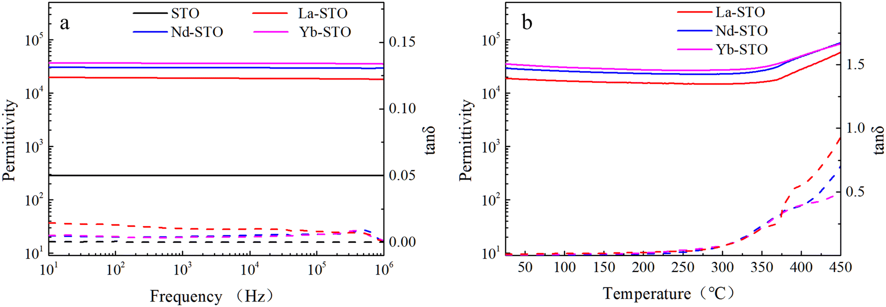
The dielectric properties of STO single crystals before and after doping are shown in Fig. 4a. All crystals exhibit frequency-independent dielectric properties. The dielectric constant of doped crystals is more than 2 × 10⁴, which is two orders of magnitude higher than that of undoped STO crystal, and the dielectric constant increases with the decrease of doped ion radius. Although the dielectric loss of doped crystals is slightly higher than that of the undoped STO crystal, it is still less than 0.015. The best dielectric properties are obtained in Yb-STO, with a dielectric constant of 3.6 × 10⁴ and dielectric loss of 0.0036 at 1 kHz. Fig. 4b shows the temperature dependence of the dielectric constant and dielectric loss of doped crystals at 1 kHz. The dielectric properties of all samples show good thermal stability over a wide temperature range (25–310 °C). The dielectric constant of all samples decreases slowly with the increase of temperature and begins to increase rapidly at about 350 °C, while the dielectric loss increases slowly at first and then sharply with the increase of temperature. In brief, the dielectric properties of the doped crystals have been significantly improved. However, there are still differences among these samples, indicating that the difference of doping ions has an important influence on the dielectric properties of STO single crystals.
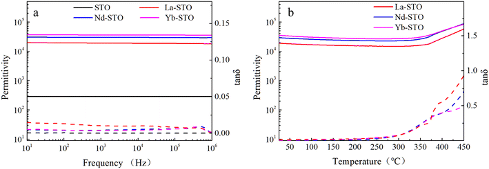 |
| | Fig. 4 (a) Frequency dependence and (b) temperature dependence (1 kHz) of permittivity and dielectric loss for STO single crystals with different doping. | |
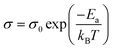
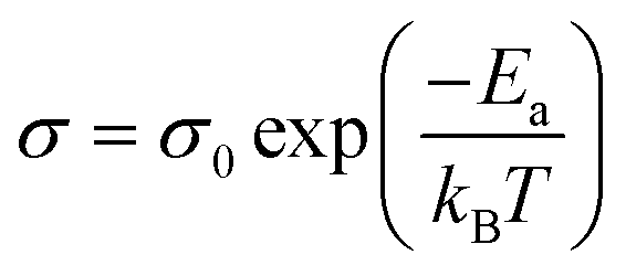
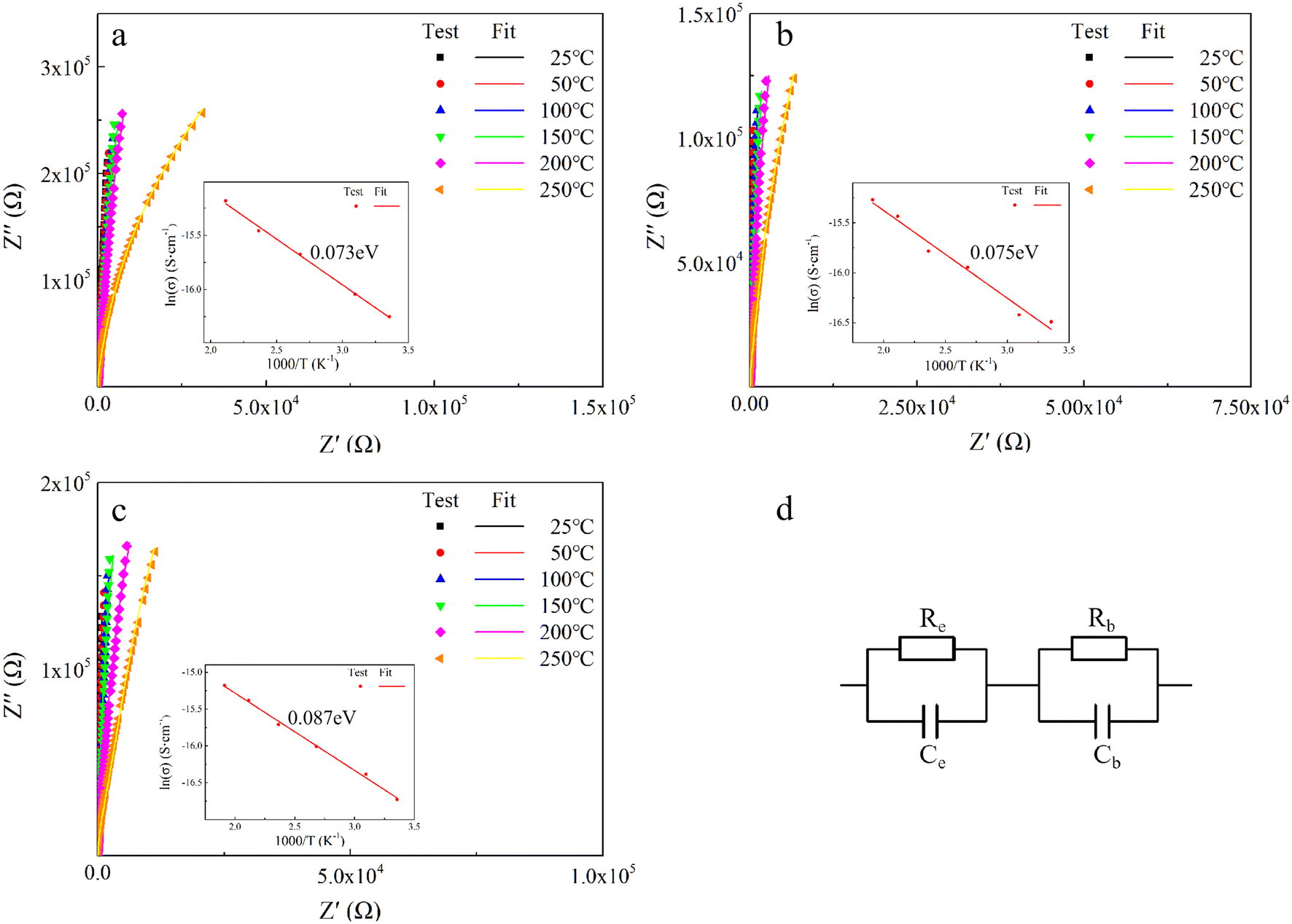
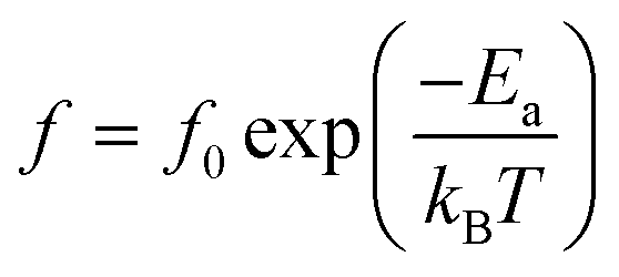
In order to explore the effect of different doping ions on the dielectric properties of STO single crystals, we use complex impedance analysis to establish the relationship between the micro-structure and the electrical properties.58Fig. 5 shows the impedance spectra of Sr99%RE1%TiO3 (RE = La, Nd, Yb) single crystals at various temperatures. The presence of non-zero intercepts at high frequencies is not observed in any of the samples, again confirming that no grain boundary effects are responsible for the excellent dielectric properties. Considering the possible influence of weak electrode effects, the circuit diagram shown in Fig. 5d is used for fitting,59 where Rb, Re, Cb and Ce represent bulk resistance, electrode contact resistance, bulk capacitance and electrode contact capacitance, respectively. The fitted results show that Yb-STO has the largest resistance value. This is because the replacement of Sr2+ by trivalent rare earth dopant ions introduces excess electrons, while Yb3+ doping partially replaces Ti4+ and reduces the number of free electrons. Rb decreases with increasing temperature for all samples, indicating that this is a thermally activated process, and Ea can be calculated by the Arrhenius law:60
| |  | (1) |
where
σ0 is a pre-exponential term,
Ea is the activation energy,
kB is the Boltzmann constant, and
T is absolute temperature (K). The activation energies of La-STO, Nd-STO and Yb-STO single crystals are 0.073 eV, 0.075 eV and 0.087 eV, respectively, which are comparable to the activation energies of conductivity caused by bound electrons, again excluding the effect of grain boundary effects.
61 La-STO and Nd-STO single crystals exhibit similar activation energies, which is due to the same doping concentration and close number of free electrons. However, the activation energy of the Nd-STO single crystal is slightly larger due to the greater distortion caused by the substitution of Nd
3+ for Sr
2+, which has a greater effect on electron binding. The Yb-STO single crystal exhibits the maximum activation energy which, on the one hand, is due to the partial substitution of Yb
3+ for Ti
4+ that reduces the number of free electrons, and on the other hand, is due to the substitution of Yb
3+ doping for both Sr
2+ and Ti
4+, which form more complex defects, and has a stronger effect on free electron binding.
 |
| | Fig. 5 Impedance spectra of Sr99%RE1%TiO3 single crystals at various temperatures: (a) La-STO, (b) Nd-STO and (c) Yb-STO. Insets are dc conductivity activation energy fitted by the Arrhenius equation. (d) Equivalent circuit diagram. | |
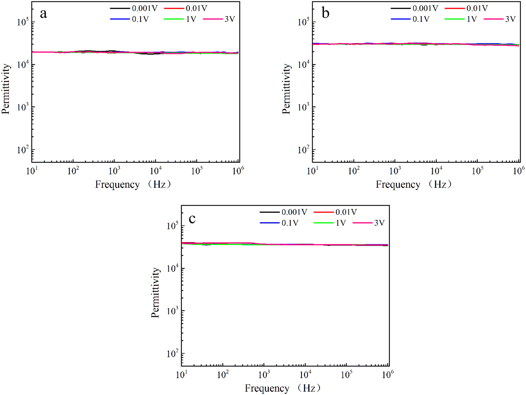
After excluding the effect of grain boundaries on the dielectric properties, considering that the interfacial polarization associated with the electrodes may be responsible for the improvement of the dielectric properties, the dielectric constants of Sr99%RE1%TiO3 single crystals were tested at different voltages. If the interfacial effects associated with the electrodes have an effect on the dielectric properties, the dielectric constant will increase sharply at low frequencies with increasing DC bias because the barrier height between the heterogeneous interfaces becomes asymmetric.62 As shown in Fig. 6, the dielectric constants of all samples remained stable under different voltages, indicating that the interfacial effects associated with the electrodes is not the main cause of the improved dielectric properties.63
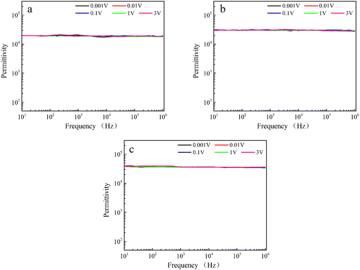 |
| | Fig. 6 Frequency-dependent dielectric properties measured under different DC bias voltages for Sr99%RE1%TiO3 single crystals: (a) La-STO crystal, (b) Nd-STO crystal and (c) Yb-STO crystal. | |
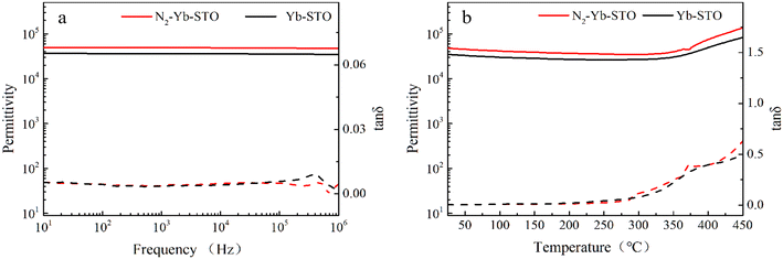
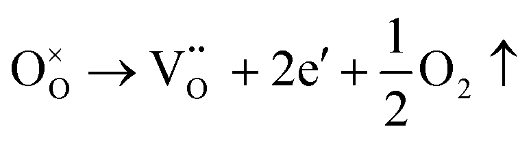
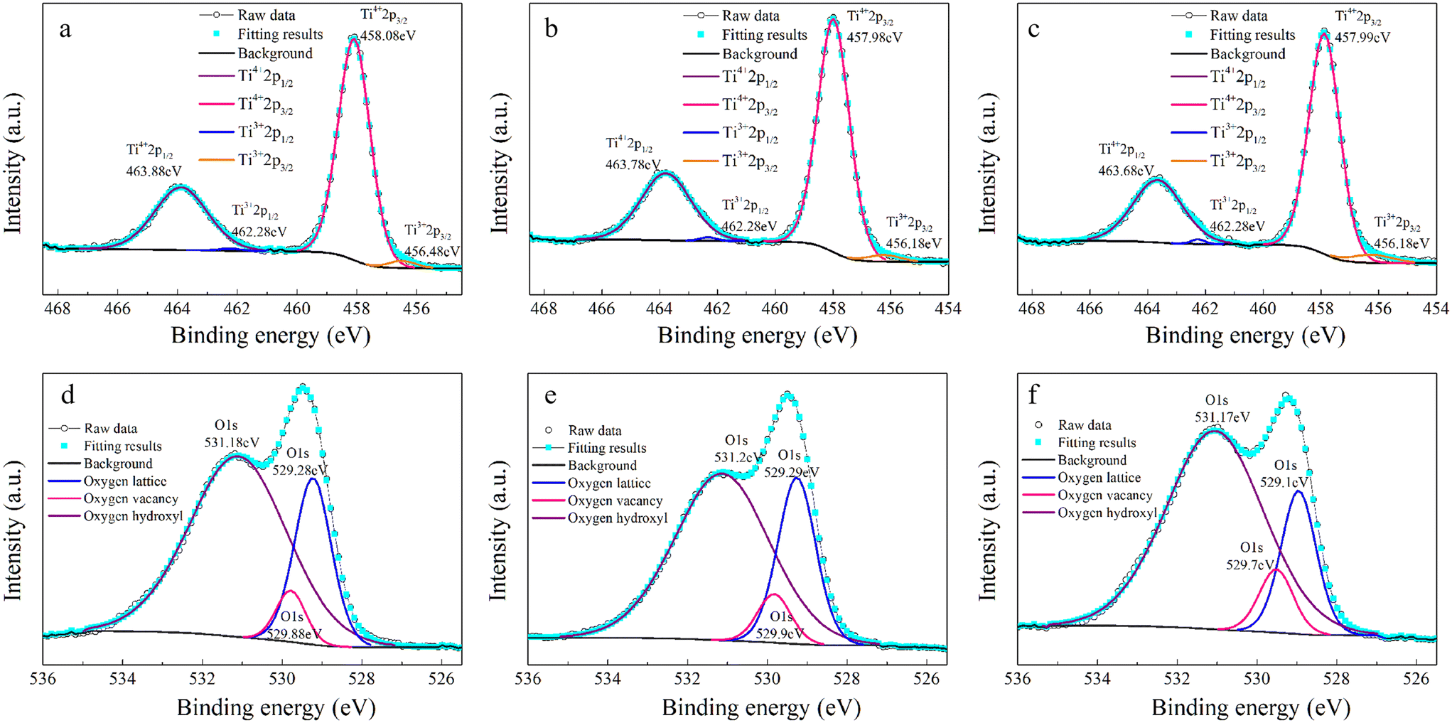
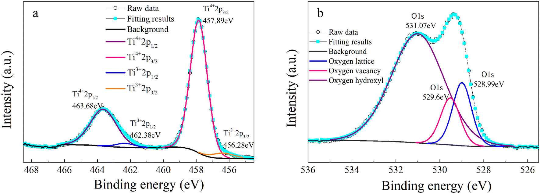
Another reason for the improved dielectric properties is the defect associated with oxygen vacancies. In order to investigate the structure of defects associated with oxygen vacancies, Sr99%RE1%TiO3 (RE = La, Nd, Yb) single crystals were analyzed using XPS. The XPS spectra and corresponding fitting results of Ti 2p and O 1s are displayed in Fig. 7. The presence of Ti3+ and oxygen vacancies is detected in all samples. The peaks at about 458.0 eV and 463.8 eV represent Ti4+, and the peaks at about 456.2 eV and 462.3 eV represent Ti3+.42 Additionally, the peaks at about 529.2 eV represents the Ti–O bond, the peak at about 529.8 eV represents the oxygen vacancy, and the peak at about 531.2 eV represents the H2O of the adsorbed surface.64,65 It was obvious that the content of Ti3+ and oxygen vacancies increases as the radius of doped ions decreases. For La-STO and Nd-STO single crystals, the trivalent Re atoms mainly replace Sr2+, introducing an extra electron which is responsible for the charge transfer from Ti4+ to Ti3+, as shown in the following equations:
| |  | (2) |
| |  | (3) |
The Nd-STO single crystal can cause greater lattice distortion and thus increase the number of defects, resulting in a slightly higher Ti
3+ and oxygen vacancy content. As for the Yb-STO single crystal, on the one hand, the trivalent Yb
3+ atom replaces Sr
2+ and introduces excess electrons, making Ti
4+ convert to Ti
3+, and on the other hand, the trivalent Yb
3+ replaces Ti
4+, requiring oxygen vacancies to compensate for the charge. In addition, lattice oxygen will overflow to form oxygen vacancies at high temperature, as shown in the following equations:
| |  | (4) |
| |  | (5) |
The greater difference in ionic radii between Yb
3+ and Sr
2+ will cause greater lattice distortion, resulting in more Ti
3+ and oxygen vacancies. In addition, as some Yb
3+ replaces Ti
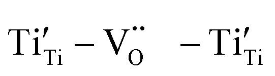
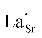
4+, some Sr vacancies will be formed. In La-STO and Nd-STO single crystals, point defects such as

,

and

are present, and in the Yb-STO single crystal, the point defects should be

,

,

,

and

. These differences cause the different polarizations and thus the difference in dielectric properties.
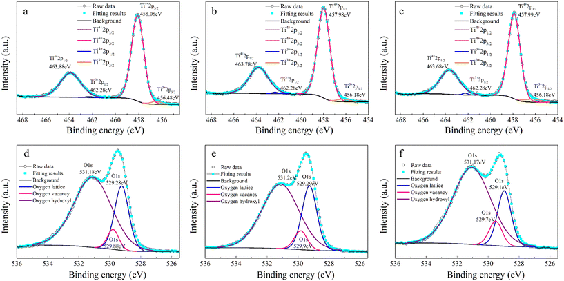 |
| | Fig. 7 XPS results of Ti and O in Sr99%RE1%TiO3 single crystals: (a) and (d) La-STO crystal, (b) and (e) Nd-STO crystal, and (c) and (f) Yb-STO crystal. | |
By studying the dielectric properties at different temperatures, the polarization process can be clearly understood. The temperature-dependent dielectric spectra are shown in Fig. 8. The dielectric constant of all samples show a similar response with temperature, decreasing and then increasing with increasing temperature over the measurement range. The dielectric loss of all samples remained below 0.1 in the range of room temperature to about 280 °C over the measured frequency range. A set of relaxation peaks can be observed for all samples in the range of 70 °C to 250 °C, and the peaks move towards high frequencies with increasing temperature, indicating a thermally activated process. The activation energy can be calculated by the Arrhenius-type equation:
| |  | (7) |
where
Ea is the activation energy,
f0 is a constant,
kB is the Boltzmann constant,
T is absolute temperature (K).
f can be obtained at the relaxation peak of tan
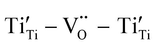
δ. The relaxation activation energies of 0.73 eV and 0.72 eV for La-STO and Nd-STO single crystals, respectively, are close to the second-order ionization energy of V˙˙, indicating that this relaxation behavior is due to defects associated with oxygen vacancies.
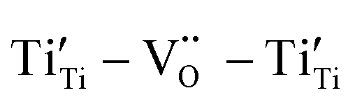
38,66 Considering the type of point defects present in the samples, this relaxation may be related to the

defect dipole clusters and
defect dipole clusters. The Yb-STO single crystal exhibits a larger activation energy of 0.89 eV, which is caused by the coupling of

and

to form a new defect dipole cluster

in addition to
and
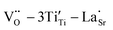
defect dipole clusters. Meanwhile, the presence of the defect dipole cluster

enables the Yb-STO single crystal to obtain better dielectric properties.
 |
| | Fig. 8 Temperature dependence of dielectric properties and plot of lnf versus 1000/T for Sr99%RE1%TiO3 single crystals with RE = La (a–c), RE = Nd (d–f), and RE = Yb (g–i). | |
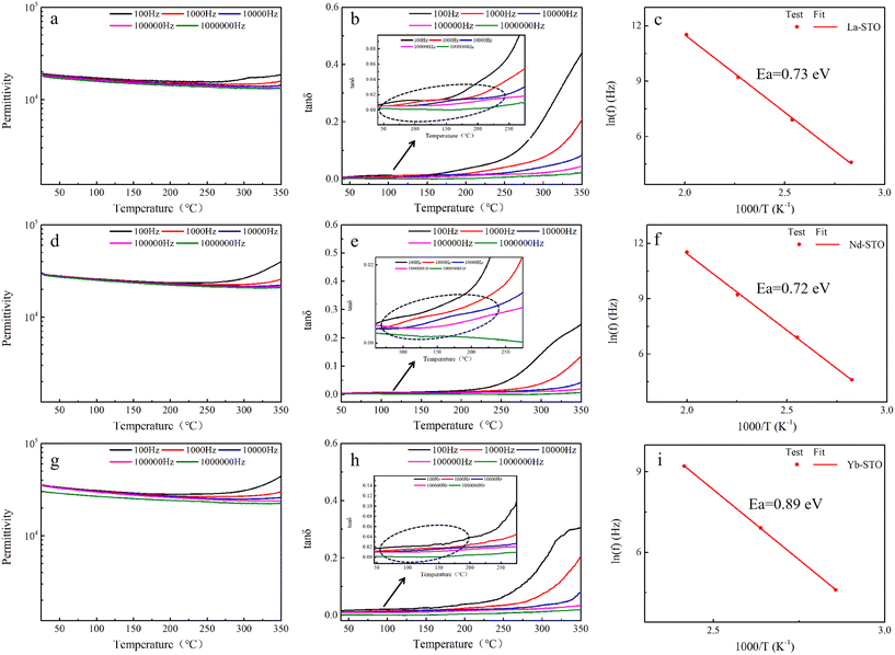
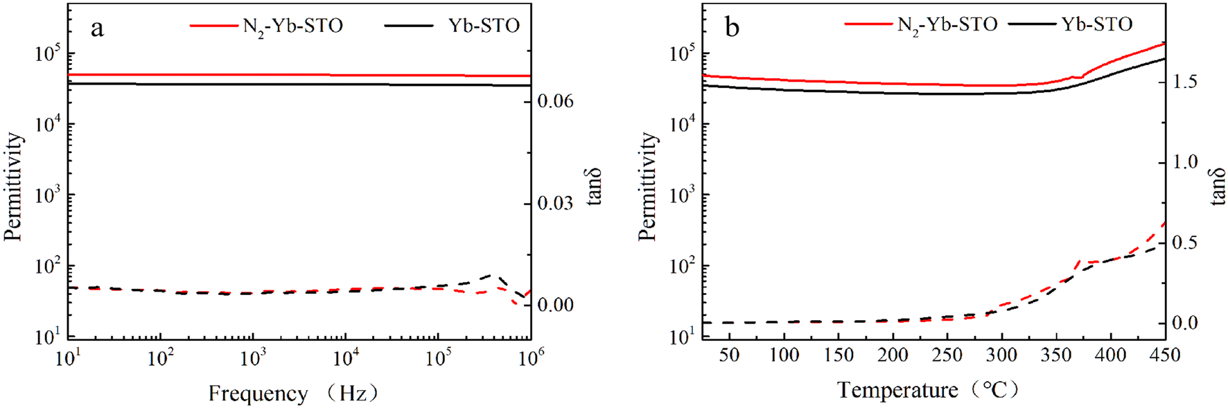
The Yb-STO single crystal with better dielectric properties was selected to study the dielectric properties after N2 annealing. As shown in Fig. 9, the dielectric constant of N2-Yb-STO has improved significantly, increasing by 34% compared to Yb-STO, and lower dielectric loss was obtained in the high frequency. At the same time, good frequency stability and temperature stability are maintained. The XPS spectra of Ti 2p and O 1s of N2-Yb-STO and their fitting results are shown in Fig. 10. The presence of Ti3+ and oxygen vacancies can be clearly observed, and their content has increased significantly compared to that before N2 annealing.67 This indicates that the enhancement of dielectric properties of the N2-Yb-STO single crystal is closely related to the oxygen vacancy concentration. The N2-Yb-STO crystal contains more oxygen vacancies, Ti3+ and other point defects, and they couple with each other to form defect complexes or clusters, which can greatly increase the dielectric constant. At the same time, these defect clusters can better localize the electrons, thus obtaining a lower dielectric loss.
 |
| | Fig. 9 (a) Frequency dependence and (b) temperature dependence (1 kHz) of permittivity and dielectric loss for N2-Yb-STO and Yb-STO single crystals. | |
 |
| | Fig. 10 XPS results of (a) Ti and (b) O in the N2-Yb-STO single crystal. | |
Fig. 11 illustrates the mechanism of obtaining excellent dielectric properties of RE-doped STO single crystals. For La-STO and Nd-STO, the excellent dielectric properties are mainly caused by defects associated with oxygen vacancies including 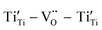 defect dipole clusters and
  defect dipole clusters. These defects generate an electron pinning effect, which localizes free electrons and hinders their long-range transition. For the Yb-STO crystal, in addition to these defect dipoles, new defect dipoles
  are formed, and these defect dipoles work together to obtain superior dielectric properties. In addition, annealing under N2 atmosphere promotes the production of oxygen vacancies and Ti3+, forming more defect dipoles, thus further optimizing the dielectric properties.
 |
| | Fig. 11 Mechanism of obtaining excellent dielectric properties:(a) La-STO crystal, (b) Nd-STO crystal and (c) Yb-STO crystal. | |
4. Conclusions
Sr99%RE1%TiO3 (RE = La, Nd, Yb) single crystals were prepared by the Verneuil method and their dielectric properties were studied. For the La-STO and Nd-STO crystals, the RE ions are substituted for Sr2+ only, and the excellent dielectric properties are mainly caused by defect dipole associated with oxygen vacancies, including  and
and 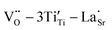 defect dipole clusters. Lattice distortion of the Nd-STO crystal is larger than that of the La-STO crystal, and thus the amount of defects is larger, resulting in better dielectric properties. For the Yb-STO crystal, some Yb3+ replaced Ti4+, forming an additional defect dipole
  , resulting in the best dielectric properties (ε′ = 3.6 × 10⁴, tanδ = 0.0036 under 1 kHz). In addition, annealing under N2 atmosphere promotes the production of oxygen vacancies and Ti3+, forming more defect dipoles, thus further improving the dielectric properties. This work suggests that the dielectric properties of RE-doped SrTiO3 materials are closely related to oxygen vacancies and that the simultaneous substitution of Sr2+ and Ti4+ may be able to obtain superior dielectric properties compared to the substitution of Sr2+ only. This is of great significance to the development of SrTiO3-based dielectric materials.
Author contributions
W. L. designed and performed the experiment with the help of S. X. D. and M. Z. X. B. X. G. and L. X. D. provided help with crystal growth. Z. M. and L. J. S. provided help with property testing. W. L. wrote the manuscript with the help of S. X. D and C. J. L. S. X. D., C. J. L. and L. J. S. provided financial support for the whole experiment. All authors have approved the final version of the manuscript.
Conflicts of interest
The authors declare no competing financial interest.
Acknowledgements
This work was supported by the Projects of the National Natural Science Foundation of China (No. 51872033 and No. 51732007), the Project of the Natural Science Foundation of Liaoning Province (No. 2019-ZD-0572), the Natural Science Foundation of Hebei Province (Grant No. E2021501017), the Young Talents Program of Hebei Province (Grant No. BJ2020202), and the Fund of the State Key Laboratory of Advanced Technologies for Comprehensive Utilization of Platinum Metals (SKL-SPM-202016 and SKL-SPM-202019).
References
- C. C. Homes and T. Vogt, Colossal permittivity materials doping for superior dielectrics, Nat. Mater., 2013, 12, 782–783, DOI:10.1038/nmat3744.
- S. Krohns, P. Lunkenheimer, S. Meissner, A. Reller, B. Gleich, A. Rathgeber, T. Gaugler, H. U. Buhl, D. C. Sinclair and A. Loidl, The route to resource-efficient novel materials, Nat. Mater., 2011, 10, 899–901, DOI:10.1038/nmat3180180.
- Y. B. Wang, W. J. Jie, C. Yang, X. H. Wei and J. H. Hao, Colossal permittivity materials as superior dielectrics for diverse applications, Adv. Funct. Mater., 2019, 29, 1808118, DOI:10.1002/adfm.201808118.
- T. T. Fang and C. P. Liu, Evidence of the internal domains for inducing the anomalously high dielectric constant of CaCu3Ti4O12, Chem. Mater., 2005, 17, 5167–5171, DOI:10.1021/cm051180k.
- P. F. Liang, Z. P. Yang, X. L. Chao and Z. H. Liu, Giant dielectric constant and good temperature stability in Y2/3Cu3TiO12 ceramics, J. Am. Ceram. Soc., 2012, 95, 2218–2225, DOI:10.1111/j.1551-2916.2012.05152.x.
- P. Thongbai, B. Putasaeng, T. Yamwong and S. Maensiri, Modified giant dielectric properties of samarium doped CaCu3Ti4O12 ceramics, Mater. Res. Bull., 2012, 47, 2257–2263, DOI:10.1016/j.materresbull.2012.05.058.
- J. J. Liu, C. G. Duan, W. G. Yin, W. N. Mei, R. W. Smith and J. R. Hardy, Large dielectric constant and Maxwell-Wagner relaxation in Bi2/3Cu3Ti4O12, Phys. Rev. B: Condens. Matter Mater. Phys., 2004, 70, 144106, DOI:10.1103/PhysRevB.70.144106.
- Z. Raddaoui, R. Lahouli, S. E. L. Kossi, J. Dhahri, K. Khirouni and K. Taibi, Effect of oxygen vacancies on dielectric properties of Ba(1-x)Nd(2x/3)TiO3 compounds, J. Alloys Compd., 2019, 771, 67–78, DOI:10.1016/j.jallcom.2018.08.242.
- V. Paunovic and L. Zivkovic, Influence of rare-earth additives (La, Sm and Dy) on the microstructure and dielectric properties of doped BaTiO3 ceramics, Sci. Sintering, 2010, 42, 69–79, DOI:10.2298/SOS1001069P.
- M. T. Buscaglia, M. Viviani, V. Buscaglia, L. Mitoseriu, A. Testino, P. Nanni, Z. Zhao, M. Nygren, C. Harnagea, D. Piazza and C. Galassi, High dielectric constant and frozen macroscopic polarization in dense nanocrystalline BaTiO3 ceramics, Phys. Rev. B: Condens. Matter Mater. Phys., 2006, 73, 064114, DOI:10.1103/PhysRevB.73.064114.
- A. A. Dakhel, Giant dielectric permittivity in Li and Pr co-doped NiO ceramics, J. Alloys Compd., 2009, 488, 31–34, DOI:10.1016/j.jallcom.2009.08.155.
- J. B. Wu, C. W. Nan, Y. H. Lin and Y. Deng, Giant dielectric permittivity observed in Li and Ti doped NiO, Phys. Rev. Lett., 2002, 89, 217601, DOI:10.1103/PhysRevLett.89.217601.
- W. B. Hu, Y. Liu, R. L. Withers, T. J. Frankcombe, L. Noren, A. Snashall, M. Kitchin, P. Smith, B. Gong, H. Chen, J. Schiemer, F. Brink and J. Wong-Leung, Electron-pinned defect-dipoles for high-performance colossal permittivity materials, Nat. Mater., 2013, 12, 821–826, DOI:10.1038/nmat3691.
- T. Nachaithong, P. Kidkhunthod, P. Thongbai and S. Maensiri, Surface barrier layer effect in (In+ Nb) co-doped TiO2 ceramics: an alternative route to design low dielectric loss, J. Am. Ceram. Soc., 2017, 100, 1452–1459, DOI:10.1111/jace.14688.
- W. Dong, W. B. Hu, A. Berlie, K. Lau, H. Chen, R. L. Withers and Y. Liu, Colossal dielectric behavior of Ga+Nb co-doped rutile TiO2, ACS Appl. Mater.
Interfaces, 2015, 7, 25321–25325, DOI:10.1021/acsami.5b07467.
- L. Wang, X. D. Liu, X. G. Bi, Z. X. Ma, J. S. Li and X. D. Sun, Origin of Colossal Dielectric Permittivity in (Nb+Ga) Co-Doped TiO2 Single Crystals, Cryst. Growth Des., 2021, 21, 5283–5291, DOI:10.1021/acs.cgd.1c00611.
- Z. Wang, M. Cao, Z. Yao, Q. Zhang, Z. Song, W. Hu, Q. Xu, H. Hao, H. Liu and Z. Yu, Giant permittivity and low dielectric loss of SrTiO3 ceramics sintered in nitrogen atmosphere, J. Eur. Ceram. Soc., 2014, 34, 1755–1760, DOI:10.1016/j.jeurceramsoc.2014.01.015.
- J. Xie, H. Hao, H. Liu, Z. Yao, Z. Song, L. Zhang, Q. Xu, J. Dai and M. Cao, Dielectric relaxation behavior and energy storage properties of Sn modified SrTiO3 based ceramics, Ceram. Int., 2016, 42, 12796–12801, DOI:10.1016/j.ceramint.2016.05.042.
- Z. Dai, S. Guo, Y. Gong and Z. Wang, Semiconductor flexoelectricity in graphite-doped SrTiO3 ceramics, Ceram. Int., 2021, 47, 6535–6539, DOI:10.1016/j.ceramint.2020.10.239.
- B. G. Kim, S. M. Cho, T. Y. Kim and H. M. Jang, Giant dielectric permittivity observed in Pb-based perovskite ferroelectrics, Phys. Rev. Lett., 2001, 86, 3404–3406, DOI:10.1103/PhysRevLett.86.3404.
- M. A. Subramanian, L. Dong, N. Duan, B. A. Reisner and A. W. Sleight, High dielectric constant in ACu3Ti4O12 and ACu3Ti3FeO12 phases, J. Solid State Chem., 2000, 151, 323–325, DOI:10.1006/jssc.2000.8703.
- J. Khemprasit and B. Khumpaitool, Influence of Cr doping on structure and dielectric properties of LixCryNi1−x−yO ceramics, Ceram. Int., 2015, 41, 663–669, DOI:10.1016/j.ceramint.2014.08.119.
- W. Li, Z. Liu, F. Zhang, Q. Sun, Y. Liu and Y. Li, Colossal permittivity of (Li, Nb) co-doped TiO2 ceramics, Ceram. Int., 2019, 45, 11920–11926, DOI:10.1016/j.ceramint.2019.03.080.
- C. C. Homes, T. Vogt, S. M. Shapiro, S. Wakimoto and A. P. Ramirez, Optical response of high-dielectric-constant perovskite-related oxide, Science, 2001, 293, 673–676, DOI:10.1126/science.1061655.
- J. L. Li, F. Li, Y. Y. Zhuang, L. Jin, L. H. Wang, X. Y. Wei, Z. Xu and X. J. Zhang, Microstructure and dielectric properties of (Nb+In) co-doped rutile TiO2 ceramics, J. Appl. Phys., 2014, 116, 074105, DOI:10.1063/1.4893316.
- T. B. Adams, D. C. Sinclair and A. R. West, Characterization of grain boundary impedances in fine- and coarse-grained CaCu3Ti4O12 ceramics, Phys. Rev. B: Condens. Matter Mater. Phys., 2006, 73, 094124, DOI:10.1103/PhysRevB.73.094124.
- S. N. I. Burn, Dielectric properties of donor-doped polycrystalline SrTiO3, J. Mater. Sci., 1982, 17, 3510–3524, DOI:10.1007/BF00752196.
- Z. W. Li, J. G. Wu, D. Q. Xiao, J. G. Zhu and W. J. Wu, Colossal permittivity in titanium dioxide ceramics modified by tantalum and trivalent elements, Acta Mater., 2016, 103, 243–251, DOI:10.1016/j.actamat.2015.09.046.
- W. Dong, W. B. Hu, T. J. Frankcombe, D. H. Chen, C. Zhou, Z. X. Fu, L. Candido, G. Q. Hai, H. Chen, Y. X. Li, R. L. Withersa and Y. Liu, Colossal permittivity with ultralow dielectric loss in In+Ta Co-doped rutile TiO2, J. Mater. Chem. A, 2017, 5, 5436–5441, 10.1039/C6TA08337D.
- Z. W. Li, X. Luo, W. J. Wu and J. G. Wu, Niobium and divalent-modified titanium dioxide ceramics: colossal permittivity and composition design, J. Am. Ceram. Soc., 2017, 100, 3004–3012, DOI:10.1111/jace.14850.
- K. Van Benthem, C. Elsässer and R. H. French, Bulk electronic structure of SrTiO3: Experiment and theory, J. Appl. Phys., 2001, 90, 6156–6164, DOI:10.1063/1.1415766.
- Z. Wang, M. Cao, Q. Zhang, H. Hao, Z. Yao, Z. Wang, Z. Song, Y. Zhang, W. Hu, H. Liu and S. Zhang, Dielectric relaxation in Zr-doped SrTiO3 ceramics sintered in N2 with giant permittivity and low dielectric loss, J. Am. Ceram. Soc., 2015, 98, 472–482, DOI:10.1111/jace.13288.
- A. Tkach, P. M. Vilarinho, A. L. Kholkin, A. Pashkin, P. Samoukhina, J. Pokorny, S. Veljko and J. Petzelt, Lattice dynamics and dielectric response of Mg-doped SrTiO3 ceramics in a wide frequency range, J. Appl. Phys., 2005, 97, 044104–044106, DOI:10.1063/1.1849822.
- M. E. Guzhva, V. V. Lemanov, P. A. Markovin and W. Kleemann, Critical concentrations in Ba-doped incipient ferroelectric SrTiO3, Phys. Solid State, 1997, 39, 618–624, DOI:10.1134/1.1129941.
- J. G. Bednorz and K. A. Müller, Sr1-xCaxTiO3: an XY quantum ferroelectric with transition to randomness, Phys. Rev. Lett., 1984, 52, 2289–2292, DOI:10.1103/PhysRevLett.52.2289.
- C. C. Wang, C. M. Lei, G. J. Wang, X. H. Sun, T. Li, S. G. Huang, H. Wang and Y. D. Li, Oxygen-vacancy-related dielectric relaxations in SrTiO3 at high temperatures, J. Appl. Phys., 2013, 113, 392, DOI:10.1063/1.4794349.
- Z. Y. Shen, Q. G. Hu, Y. M. Li, Z. M. Wang, W. Q. Luo, Y. Hong, Z. X. Xie and R. H. Liao, Structure and dielectric properties of Re0.02Sr0.97TiO3 (Re=La, Sm, Gd, Er) ceramics for high-voltage capacitor applications, J. Am. Ceram. Soc., 2013, 96, 2551–2555, DOI:10.1111/jace.12364.
- X. Zhou, M. Cao, Z. Wang, Y. Rao, Q. Luo, B. Yang, H. Hao, Z. Yao, Z. Yu and H. Liu, Defect chemistry and dielectric behavior of Sr0.99Ce0.01Ti1−xO3 ceramics with high permittivity, Ceram. Int., 2018, 44, 12065–12072, DOI:10.1016/j.ceramint.2018.03.221.
- A. Tkach, O. Okhay, A. Almeida and P. M. Vilarinho, Giant dielectric permittivity and high tunability in Y-doped SrTiO3 ceramics tailored by sintering atmosphere, Acta Mater., 2017, 130, 249–260, DOI:10.1016/j.actamat.2017.03.051.
- Z. Wang, Z. Wang, M. Cao, Z. Yao, H. Hao, Z. Song, X. Huang, W. Hu and H. Liu, Structures and dielectric properties of Sr0.9775Sm0.015TiO3 ceramics sintered in N2, Ceram. Int., 2015, 41, 12945–12949, DOI:10.1016/j.ceramint.2015.06.137.
- Z. Y. Shen, Q. G. Hu, Y. M. Li, Z. M. Wang, W. Q. Luo, Y. Hong, Z. X. Xie and R. H. Liao, Structure and energy storage properties of Ti vacancies charge compensated Re2O3-doped SrTiO3(Re= Pr, Nd, Gd) ceramics, J. Mater. Sci.: Mater. Electron., 2013, 24, 3089–3094, DOI:10.1007/s10854-013-1215-1.
- X. Guo, Y. Pu, W. Wang, J. Ji, J. Li, M. Yang and R. Shi, Defect chemistry and colossal dielectric behavior of Nd-modified SrTiO3 lead-free ceramic materials, Ceram. Int., 2020, 46, 16644–16652, DOI:10.1016/j.ceramint.2020.03.237.
- M. Qin, F. Gao, J. Cizek, S. Yang, X. Fan, L. Zhao, J. Xu, G. Dong, M. Reece and H. Yan, Point defect structure of La-doped SrTiO3 ceramics with colossal permittivity, Acta Mater., 2019, 164, 76–89, DOI:10.1016/j.actamat.2018.10.025.
- X. Zhang, J. Zhang, Y. Zhou, Z. Yue and L. Li, Colossal permittivity and defect-dipoles contribution for Ho0.02Sr0.97TiO3 ceramics, J. Alloys Compd., 2018, 767, 424–431, DOI:10.1016/j.jallcom.2018.07.118.
- L. Wang, X. D. Liu, M. Zhang, X. G. Bi, Z. X. Ma, J. S. Li, J. L. Chen and X. D. Sun, Colossal dielectric behavior of (Nb, Ga) co-doped TiO2 single crystal, J. Alloys Compd., 2022, 921, 166053, DOI:10.1016/j.jallcom.2022.166053.
- H. Kishi, N. Kohzu, J. Sugino, H. Ohsato, Y. Iguchi and T. Okuda, The Effect of Rare-earth (La, Sm, Dy, Ho and Er) and Mg on the Microstructure in BaTiO3, J. Eur. Ceram. Soc., 1999, 19, 1043–1046, DOI:10.1016/S0955-2219(98)00370-7.
- Q. Liu, J. Liu, D. Lu and W. Zheng, Colossal dielectric behavior and relaxation in Nd-doped BaTiO3 at low temperature, Ceram. Int., 2018, 44, 7251–7258, DOI:10.1016/j.ceramint.2018.01.181.
- A. Tkach, P. M. Vilarinho, D. Nuzhnyy and J. Petzelt, Sr-and Ti-site substitution, lattice dynamics and octahedral tilt transition relationship in SrTiO3: Mn ceramics, Acta Mater., 2010, 58, 577–582, DOI:10.1016/j.actamat.2009.09.036.
- S. Bhattacharya, A. M. Dehkordi, H. N. Alshareef and T. M. Tritt, Synthesis-property relationship in thermoelectric Sr1-xYbxTiO3-δ ceramics, J. Phys. D: Appl. Phys., 2014, 47, 385302, DOI:10.1088/0022-3727/47/38/385302.
- M. Battabyal, P. Balasubramanian, P. M. Geethu, L. Pradipkanti, D. K. Satapathy and R. Gopalan, Tailoring the optical phonon modes and dielectric properties of nanocrystalline SrTiO3 via Yb doping, Mater. Res. Express, 2018, 5, 046301, DOI:10.1088/2053-1591/aabb42.
- W. Pan, M. Cao, H. Wang, A. Jan, H. Hao, Z. Yao and H. Liu, Giant dielectric response in (Nb+ Zn) co-doped strontium titanate ceramics tailored by atmosphere, Scr. Mater., 2019, 170, 166–171, DOI:10.1016/j.scriptamat.2019.05.034.
- W. G. Nilsen and J. G. Skinner, Raman spectrum of strontium titanate, J. Chem. Phys., 1968, 48, 2240, DOI:10.1063/1.1669418.
- K. Nishida, H. Kishi, M. Osada, H. Funakubo, M. Nishide, H. Takeuchi, T. Katoda and T. Yamamoto, Raman spectroscopy evaluation of oxygen vacancy migration by electrical field in multilayer ceramic capacitors, Jpn. J. Appl. Phys., 2009, 48, 09KF11, DOI:10.1143/JJAP.48.09KF11.
- J. M. Li, C. H. A. Huan, Y. W. Du, D. Feng and Z. X. Shen, Magnetic-field-tunable charge carrier localization in sintered polycrystalline La0.75Ca0.25MnO3, Phys. Rev. B: Condens. Matter Mater. Phys., 2000, 63, 024416, DOI:10.1103/PhysRevB.63.024416.
- O. Kurt, D. Ascienzo, S. Greenbaum, T. J. M. Bayer, C. A. Randall, N. Madamopoulos and Y. H. Ren, Nonlinear optical detections of structural distortions at degraded Fe-doped SrTiO3 interfaces, Mater. Chem. Phys., 2017, 198, 131–136, DOI:10.1016/j.matchemphys.2017.05.047.
- R. L. Moreira, R. P. S. M. Lobo, G. Subodh, M. T. Sebastian, F. M. Matinaga and A. Dias, Optical phonon modes and dielectric behavior of Sr1-3x/2CexTiO3 microwave ceramics, Chem. Mater., 2007, 19, 6548–6554, DOI:10.1021/cm7024747.
- Y. Yang, H. Hao, L. Zhang, C. Chen, Z. P. Luo, Z. Liu, Z. H. Yao, M. H. Cao and H. X. Liu, Structure, electrical and dielectric properties of Ca substituted BaTiO3 ceramics, Ceram. Int., 2018, 44, 11109–11115, DOI:10.1016/j.ceramint.2018.03.111.
- N. Thongyong, W. Tuichai, N. Chanlek and P. Thongbai, Effect of Zn2+ and Nb5+ co-doping ions on giant dielectric properties of rutile-TiO2 ceramics, Ceram. Int., 2017, 43, 15466–15471, DOI:10.1016/j.ceramint.2017.08.093.
- Y. L. Song, X. J. Wang, Y. Sui, Z. Y. Liu, Y. Zhang, H. S. Zhan, B. Q. Song, Z. G. Liu, Z. Lv, L. Ta and J. K. Tang, Origin of colossal dielectric permittivity of rutile Ti0.9In0.05Nb0.05O2: single crystal and polycrystalline, Sci. Rep., 2016, 6, 21478, DOI:10.1038/srep21478.
- J. T. Fan, S. L. Leng, Z. Z. Cao, W. Y. He, Y. F. Gao, J. R. Liu and G. R. Li, Colossal permittivity of Sb and Ga co-doped rutile TiO2 ceramics, Ceram. Int., 2019, 45, 1001–1010, DOI:10.1016/j.ceramint.2018.09.279.
- L. X. Li, T. Lu, N. Zhang, J. T. Li and Z. Y. Cai, The effect of segregation structure on the colossal permittivity properties of (La0.5Nb0.5)xTi1−xO2 ceramics, J. Mater. Chem. C, 2018, 6, 2283–2294, 10.1039/C7TC05277D.
- W. Tuichai, S. Danwittayakul, N. Chanlek, P. Srepusharawoot, P. Thongbai and S. Maensiri, Origin(s) of the apparent colossal permittivity in (In1/2Nb1/2)xTi1−xO2: clarification on the strongly induced Maxwell–Wagner polarization relaxation by DC bias, RSC Adv., 2017, 7, 95–105, 10.1039/C6RA26728A.
- C. Yang, M. Y. Tse, X. H. Wei and J. H. Hao, Colossal permittivity of (Mg+ Nb) co-doped TiO2 ceramics with low dielectric loss, J. Mater. Chem. C, 2017, 5, 5170–5175, 10.1039/C7TC01020F.
- J. M. Li and Y. B. Hu, O2 atmospheric annealing-tunable defects in ionic oxide MgO nanoribbons, Appl. Phys. Lett., 2019, 114(20), 203101, DOI:10.1063/1.5099244.
- J. M. Li, X. L. Zeng, Y. H. Dong and Z. A. Xu, White-light emission and weak antiferromagnetism from cubic rare-earth oxide Eu2O3 electrospun nanostructures, CrystEngComm, 2013, 15, 2372–2377, 10.1039/C3CE26770A.
- X. Guo, Y. P. Pu, W. Wang, L. Zhang, J. M. Ji, R. K. Shi, Y. Shi, M. D. Yang and J. Li, High insulation resistivity and ultralow dielectric loss in La-doped SrTiO3 colossal permittivity ceramics through defect chemistry optimization, ACS Sustainable Chem. Eng., 2019, 7, 13041–13052, DOI:10.1021/acssuschemeng.9b02143.
- K. Uematsu, O. Sakurai, N. Mizutani and M. Kato, Electrical properties of La-doped SrTiO3 (La: 0.1 to 2.0 at %) single crystals grown by xenon-arc image floating zone method, J. Mater. Sci., 1984, 19, 3671–3679, DOI:10.1016/0022-4596(91)90363-M.
|
| This journal is © The Royal Society of Chemistry 2023 |
Click here to see how this site uses Cookies. View our privacy policy here. 
 *c,
Jinsheng
Li
d,
Mu
Zhang
*c,
Jinsheng
Li
d,
Mu
Zhang
 and
and  defect dipole clusters. For Yb-STO, Yb3+ partially replaces Ti4+, forming an additional defect dipole
 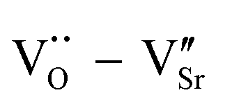 , resulting in the best dielectric properties (ε′ = 3.6 × 10⁴, tan

 ,
,  and
and 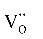 are present, and in the Yb-STO single crystal, the point defects should be
 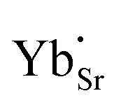 ,
,  ,
,  ,
,  and
and  . These differences cause the different polarizations and thus the difference in dielectric properties.
 defect dipole clusters and
 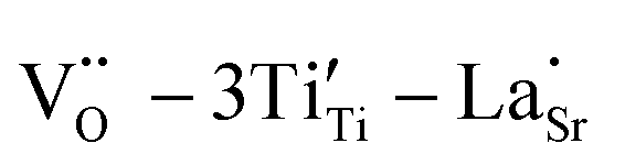 defect dipole clusters. The Yb-STO single crystal exhibits a larger activation energy of 0.89 eV, which is caused by the coupling of
 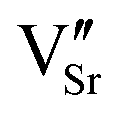 and
and  to form a new defect dipole cluster
 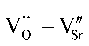 in addition to
 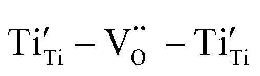 and
and  defect dipole clusters. Meanwhile, the presence of the defect dipole cluster
 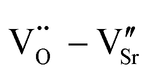 enables the Yb-STO single crystal to obtain better dielectric properties.

 defect dipole clusters and
  defect dipole clusters. These defects generate an electron pinning effect, which localizes free electrons and hinders their long-range transition. For the Yb-STO crystal, in addition to these defect dipoles, new defect dipoles
  are formed, and these defect dipoles work together to obtain superior dielectric properties. In addition, annealing under N2 atmosphere promotes the production of oxygen vacancies and Ti3+, forming more defect dipoles, thus further optimizing the dielectric properties.
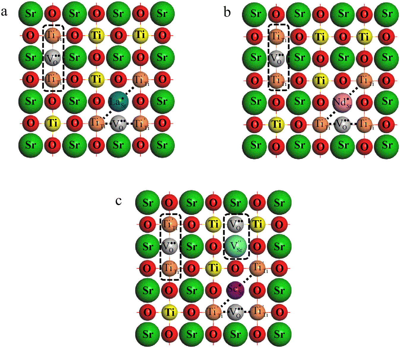
 and
and 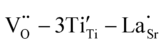 defect dipole clusters. Lattice distortion of the Nd-STO crystal is larger than that of the La-STO crystal, and thus the amount of defects is larger, resulting in better dielectric properties. For the Yb-STO crystal, some Yb3+ replaced Ti4+, forming an additional defect dipole
 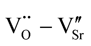 , resulting in the best dielectric properties (ε′ = 3.6 × 10⁴, tan