DOI:
10.1039/D2CE01026G
(Communication)
CrystEngComm, 2023,
25, 48-52
Revealing uncommon transport in the previously unascertained very low cation clathrate-I Eu2Ga11Sn35†
Received
26th July 2022
, Accepted 24th October 2022
First published on 24th October 2022
Abstract
High occupancy of cation sites is typical for clathrate-I compositions allowing limited tunability of the electrical properties beyond doping and elemental substitution. Herein, we report on the structure and electrical transport of single-crystal Eu2Ga11Sn35, the sole example of a very low (25%) cation concentration clathrate-I material with atypical transport directly attributable to the structure and stoichiometry.
Modification of the physical properties of materials can be realized via different doping strategies as well as alteration of the stoichiometry in certain compositions. In the latter case metal-to-semiconducting, semiconductor-to-insulating as well as metal-to-insulator transitions can be realized with stoichiometric variations.1–4 This approach can be applied to a wide variety of important applications of interest, including photovoltaics, thermoelectrics, magneto optics and magnetocaloric materials.5–8 Moreover, the pursuit of new materials employing new and unique synthetic approaches has impacted technological fields of interest.9–12 Nevertheless, molten metals employed as solvents, or fluxes, have been used for over a century in the pursuit of new compositions, as this synthesis approach allows for high diffusion rates at lower temperatures as compared to elemental reaction from the elements.13 In all these cases achieving an understanding of crystal structure and bonding, and their effects on the physical properties, is of primary importance and of fundamental interest.
A class of materials that continues to be of interest due to their diverse physical properties, as well as their potential for technological applications, is group-14 clathrates.14 One of the more engaging aspects of research on inorganic clathrates is in understanding the effects of cation occupancy, and how intermolecular and structural features modify the physical properties. This is particularly the case for low-cation concentrations. Although different compositions and structure types have been reported for some time,15,16 p-type semiconducting compositions are rare.17–23 One reason for this is the fact that clathrate-I compositions with low anion concentrations have not been realized. Thus, research on the synthesis, bonding and physical properties of inorganic clathrates has been primarily undertaken on electron-rich compositions motivated by the low thermal conductivity they possess and their potential as photovoltaic or thermoelectric materials.13,16,24–30 In electronic applications, thermoelectrics for example,31 both p and n-type materials of similar mechanical and physical properties, best obtained from like-structured materials, are required.
The clathrate-I crystal structure can be thought of as an open framework lattice formed by group-14 elements that is comprised of two dodecahedra and six tetrakaidecahedra per cubic unit cell with “guest” atoms residing inside these polyhedra formed by the framework. There are scarce reports on less-than-full cation occupancy clathrate-I compositions, and none on very low cation concentration compositions.14,32–35 Although reports on the synthesis of very low cation concentration clathrate-II compositions have been published, e.g. NaxSi136,36–40 there have not been any reports on very low cation concentration clathrate-I compositions. The thermal conductivity of these materials is expected to be low;14,17,25,29 however, the salient aspects of our work reveal that p-type semiconducting Eu2Ga11Sn35 displays atypical electronic transport that is a direct result of the structure and composition in this very low cation concentration clathrate-I composition.
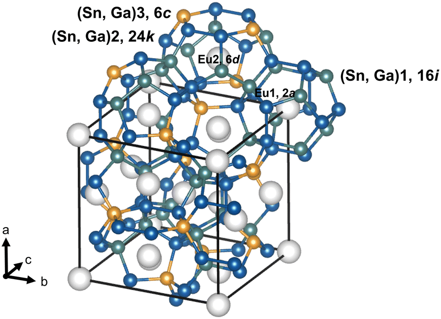
Single crystals of Eu2Ga11Sn35 were grown from Sn flux. Europium pieces (99.99%, Ames Labs), Ga pellets (99.99999%, Alfa Aesar) and Sn pieces (99.9999%, Alfa Aesar)41 in a 1![[thin space (1/6-em)]](https://www.rsc.org/images/entities/char_2009.gif) :2:12 atomic ratio were loaded into a tungsten crucible that was then sealed inside a glass tube, all synthetic procedures occurring inside a nitrogen glovebox. The glass tube was sealed under vacuum, heated to 650 °C at a rate of 25 degrees per hour, where it was held for 15 hours before slow cooling to 450 °C at a rate of 10 degrees per hour at which point it was air cooled to room temperature. A mixture of 10 mL HCl, 10 mL HNO3 and 80 mL DI water was used to remove potential residual flux from the surface of the Eu2Ga11Sn35 crystals. Several single crystals were preliminarily investigated by X-ray diffraction (XRD) employing a Bruker Smart Apex II CCD diffractometer using Mo Kα radiation. Single-crystal synchrotron data was collected with a Huber 3-circles diffractometer equipped with a Pilatus3 X 1M CdTe detector employing ChemMatCARS advanced crystallography program at the Advanced Photon Source (APS) of Argonne National Laboratory with applied absorption corrections using the Brennan method.45Fig. 1 illustrates the crystal structure. The structure was solved with the ShelXT-201443 program and refined with ShelXL-2018/3.44 Temperature-dependent electrical transport measurements were performed on a single crystal employing the Physical Property Measurements System from Quantum Design. Further structural and measurement details are provided in the ESI.†
:2:12 atomic ratio were loaded into a tungsten crucible that was then sealed inside a glass tube, all synthetic procedures occurring inside a nitrogen glovebox. The glass tube was sealed under vacuum, heated to 650 °C at a rate of 25 degrees per hour, where it was held for 15 hours before slow cooling to 450 °C at a rate of 10 degrees per hour at which point it was air cooled to room temperature. A mixture of 10 mL HCl, 10 mL HNO3 and 80 mL DI water was used to remove potential residual flux from the surface of the Eu2Ga11Sn35 crystals. Several single crystals were preliminarily investigated by X-ray diffraction (XRD) employing a Bruker Smart Apex II CCD diffractometer using Mo Kα radiation. Single-crystal synchrotron data was collected with a Huber 3-circles diffractometer equipped with a Pilatus3 X 1M CdTe detector employing ChemMatCARS advanced crystallography program at the Advanced Photon Source (APS) of Argonne National Laboratory with applied absorption corrections using the Brennan method.45Fig. 1 illustrates the crystal structure. The structure was solved with the ShelXT-201443 program and refined with ShelXL-2018/3.44 Temperature-dependent electrical transport measurements were performed on a single crystal employing the Physical Property Measurements System from Quantum Design. Further structural and measurement details are provided in the ESI.†
 |
| | Fig. 1 The Eu2Ga11Sn35 crystal structure emphasizing the clathrate-I framework (Sn/Ga)20 and (Sn/Ga)24 polyhedra. The 6c (yellow), 16i (green) and 24k (dark blue) Wyckoff sites are labelled, Sn and Ga randomly occupy all three framework sites. The structure crystallizes in the space group Pm![[3 with combining macron]](https://www.rsc.org/images/entities/char_0033_0304.gif) n with a lattice parameter of 11.9497(5) Å, as determined by single crystal synchrotron data.42 The unit cell of the structure (highlighted by black solid lines) contains Eu at the 2a and 6d sites in a 1:3 ratio, respectively. The sites of possible occupancy by Eu are displayed by light grey spheres. n with a lattice parameter of 11.9497(5) Å, as determined by single crystal synchrotron data.42 The unit cell of the structure (highlighted by black solid lines) contains Eu at the 2a and 6d sites in a 1:3 ratio, respectively. The sites of possible occupancy by Eu are displayed by light grey spheres. | |
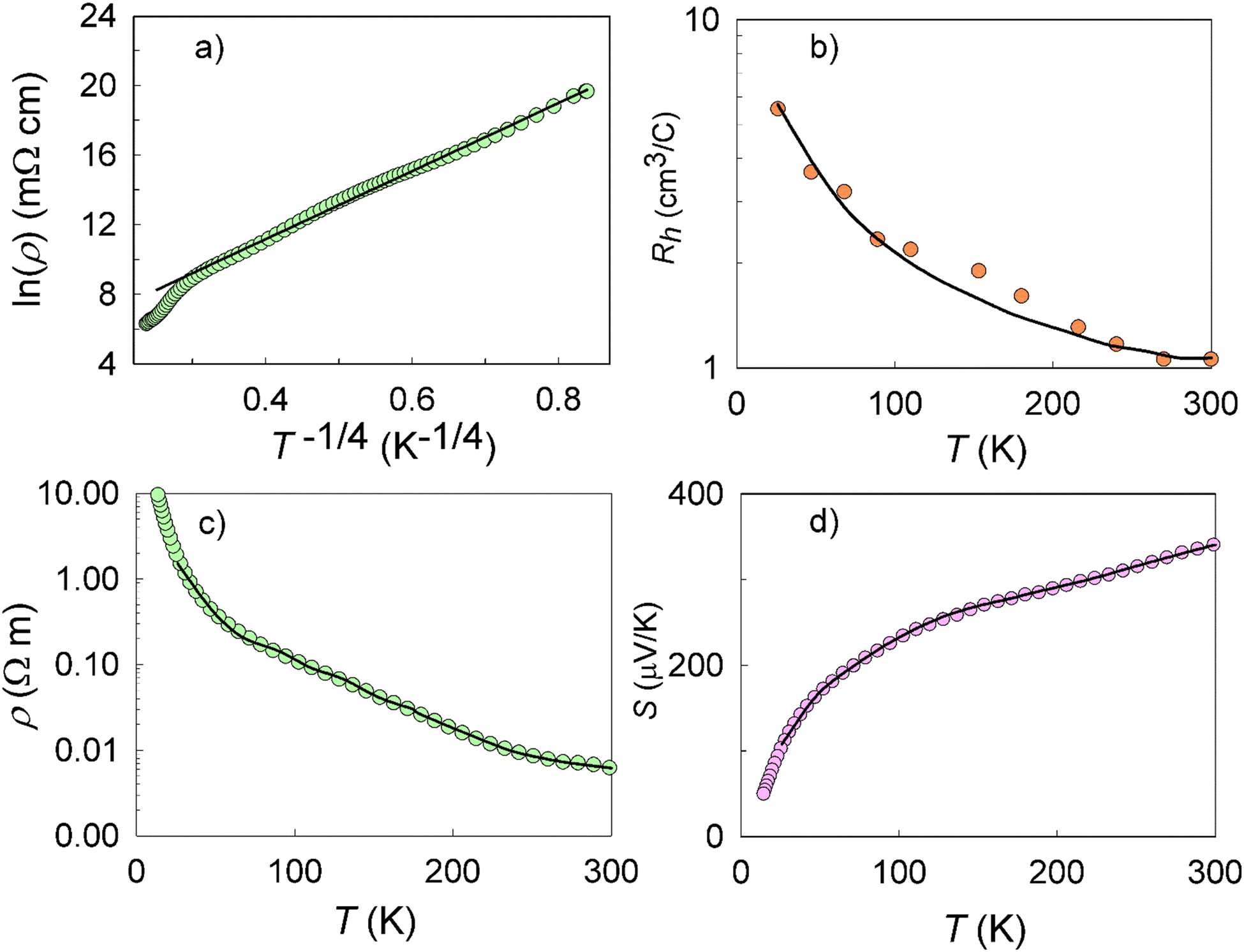
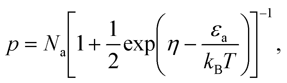
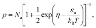
The Hall concentration, p, at room temperature (5.90 × 1018 cm−3) was much less than that expected by simple electron counting (4 × 1021 cm−3) assuming the Zintl rule with Eu providing two electrons to the framework and Ga and Sn providing three and four valence electrons, respectively. Moreover, our resistivity, ρ, measurements suggest transport via variable-range hopping (VRH) that is indicative of impurity-band conduction, as shown in Fig. 2(a). The fit to ρ = ρ0exp[(T0/T)1/4] in the figure indicates a transition from band conduction to impurity-band conduction at approximately 120 K. Hence, both valence band conduction as well as a low-mobility impurity band acceptor density, Na, is required to describe the hole transport in Eu2Ga11Sn35.46,47 Our model, which includes an impurity band with Na at energy εa above the valence-band edge, describes the transport data very well as discussed in what follows and shown in Fig. 2.
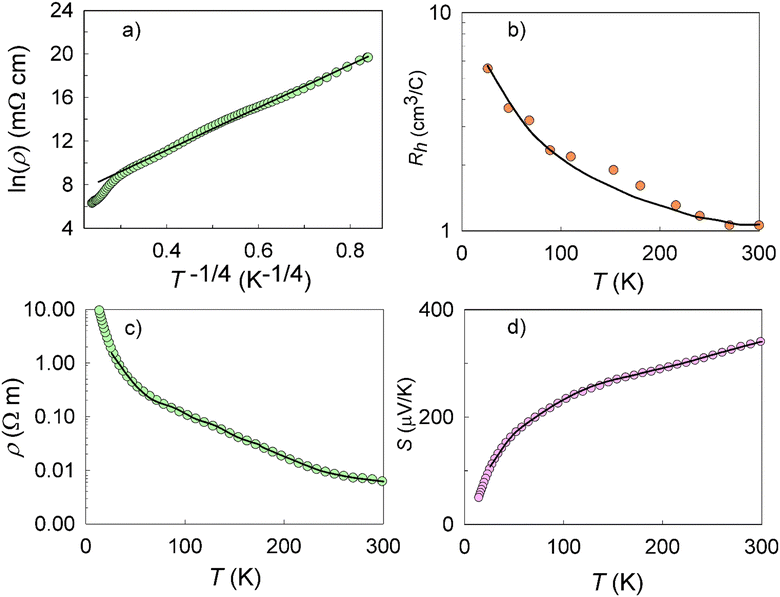 |
| | Fig. 2 (a) Ln(ρ) vs. 1/T1/4, where the solid line is a fit of the form ρ = ρ0exp[(T0/T)1/4] with ρ0 = 2.84 × 10⁻² Ω cm and T0 = 1.46 × 10⁵ K. At room temperature ρ = 620 mΩ cm. Note the ESI† where the data indicates a 0.13 eV bandgap for Eu2Ga11Sn35. Temperature-dependent (b) Hall coefficient, (c) resistivity and (d) Seebeck coefficient data with solid lines from the model described in the text. | |
For hole transport the equation for charge neutrality is
where
na is the acceptor impurity atom density.
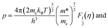
40,41 The valence band mobility (
μ) and
na can be solved simultaneously using the expressions given for
RH and
ρ, namely
| | 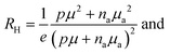 | (2) |
| | 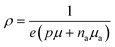 | (3) |
As shown in
Fig. 2(b)–(d), excellent agreement to the experimental Hall coefficient,
RH,
ρ, and Seebeck coefficient,
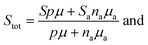
Stot, data were obtained using these expressions with
μa = 0.06 cm
2 V
−1 s
−1 in order to simplify the simultaneous analysis of all the experimental data according to the model. A weighted sum of
Stot was used with contributions from the valence band (
S) and impurity band (
Sa) given by,
| |  | (4) |
| | 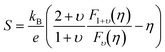 | (5) |
where
η =
ξF/
kBT,
ξF is the chemical potential measured with respect to the band edge and
υ is a constant value that is governed by the dominant scattering mechanism (
υ = 2, 0.5 and 0 for ionized impurity, neutral impurity, and acoustic phonon scattering, respectively).
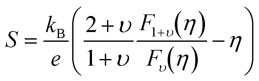
Eqn (4) simplifies to
Stot ≈
S (1 +
naμa/
pμ)
−1 since
S ≫
Sa at all temperatures other than very low temperatures. As shown in
Fig. 2 the fits agree very well with the experimental values when ionized impurity scattering (
υ = 2) is dominant throughout the entire temperature range of the
RH data. A comparison between the temperature dependent
μ values obtained from the model and temperature dependent forms of hall mobility for ionized impurity scattering (∼
T3/2), neutral impurity (∼const) and acoustic phonon scattering (∼
T−3/2) at the different
υ values described above confirmed this observation. These results also indicate the self-consistency of the model. At
υ = 2 the expressions,
| |  | (6) |
| |  | (7) |
| |  | (8) |
can be employed to calculate
m* and
εa using
η and
Na derived above resulting in
μ = 1.7 cm
2 V
−1 s
−1,
m* = 0.38
me and
Na = 5.91 × 10
18 cm
−3 at
εa = 1.6 meV above the valence band edge at room temperature. Here,
m* is the hole effective mass,
me is the free electron mass and
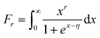
Fr is the Fermi integral of order
r. This
m* value is small, as is also the case for n-type clathrate-I compositions and reveals the relatively steep curvature of the valence band, with an acceptor density that reveals the ‘balance’ between the europium ion donors and compensation from the framework acceptors as
Na is smaller than that reported for n-type clathrate-I compositions.
14
In summary, single-crystal Eu2Ga11Sn35 was grown from tin flux allowing for intrinsic temperature-dependent electrical properties measurements and analyses. Atypical electrical transport, as compared with other clathrate compositions, is obtained for this very low cation tin clathrate-I material with transport data indicating conduction band to impurity band conduction with decreasing temperature. Our model, as described in detail above, fits the transport data very well. Our work also reinforces the impact of metallic flux crystal growth in new materials research.
The authors acknowledge financial support from the U.S. National Science Foundation (NSF) under Grant No. DMR-1748188. W. W.-N. thanks H. Joress for work during the preliminary structure study. ChemMatCARS Sector 15 was principally supported by the Divisions of Chemistry (CHE) and Materials Research (DMR), National Science Foundation, under grant number NSF/CHE-1834750. Use of the Advanced Photon Source, an Office of Science User Facility operated for the U.S. Department of Energy (DOE) Office of Science by Argonne National Laboratory, was supported by the U.S. DOE under Contract No. DE-AC02-06CH11357.
Author contributions
Wilarachchige D. C. B. Gunatilleke: investigation, formal analysis, visualization. Winnie Wong-Ng: data curation, formal analysis. Peter Y. Zavalij: data curation. Mingjian Zhang: data curation. Yu-Sheng Chen: data curation, formal analysis. George S. Nolas: conceptualization, investigation, supervision, writing – original draft, project administration.
Conflicts of interest
There are no conflicts to declare.
Notes and references
- J. M. Honig and L. L. V. Zandt, Annu. Rev. Mater. Sci., 1975, 5, 225 CrossRef CAS.
- S. Stefanoski, C. D. Malliakas, M. G. Kanatzidis and G. S. Nolas, Inorg. Chem., 2012, 51, 8686 CrossRef CAS PubMed.
- C. H. Griffiths and H. K. Eastwood, J. Appl. Phys., 1974, 45, 2201 CrossRef CAS.
- D. S. Jeong, R. Thomas, R. S. Katiyar, J. F. Scott, H. Kohlstedt, A. Petraru and C. S. Hwang, Rep. Prog. Phys., 2012, 75, 076502 CrossRef PubMed.
- J. He and T. M. Tritt, Science, 2017, 357, eaak9997 CrossRef PubMed.
- K. Tsevas, J. A. Smith, V. Kumar, C. Rodenburg, M. Fakis, A. R. B. Mohd Yusoff, M. Vasilopoulou, D. G. Lidzey, M. K. Nazeeruddin and A. D. Dunbar, Chem. Mater., 2021, 33, 554 CrossRef CAS.
- J. Y. Rhee, Y. V. Kudryavtsev and Y. P. Lee, Phys. Rev. B: Condens. Matter Mater. Phys., 2003, 68, 045104 CrossRef.
- A. De Campos, D. L. Rocco, A. M. G. Carvalho, L. Caron, A. A. Coelho, S. Gama, L. M. Da Silva, F. C. Gandra, A. O. Dos Santos, L. P. Cardoso and P. J. Von Ranke, Nat. Mater., 2006, 5, 802 CrossRef CAS.
- S. Stefanoski, M. Beekman, W. Wong-Ng, P. Zavalij and G. S. Nolas, Chem. Mater., 2011, 23, 1491 CrossRef CAS.
- L. Ye, S. Zhang, L. Huo, M. Zhang and J. Hou, Acc. Chem. Res., 2014, 47, 1595 CrossRef CAS PubMed.
- B. G. Shen, J. R. Sun, F. X. Hu, H. W. Zhang and Z. H. Cheng, Adv. Mater., 2009, 21, 4545 CrossRef CAS.
- M. G. Kanatzidis, Curr. Opin. Solid State Mater. Sci., 1997, 2, 139 CrossRef CAS.
- M. G. Kanatzidis, R. Pöttgen and W. Jeitschko, Angew. Chem., Int. Ed., 2005, 44, 6996 CrossRef CAS PubMed.
-
G. S. Nolas, The physics and chemistry of inorganic clathrates, Springer, vol. 199, 2014 Search PubMed.
- C. Cros, M. Pouchard and P. Hagenmuller, C. R. Hebd. Seances Acad. Sci., 1965, 260(18), 4764 CAS.
- J. S. Kasper, P. Hagenmuller, M. Pouchard and C. Cros, Science, 1965, 150, 1713 CrossRef CAS PubMed.
-
G. S. Nolas, G. A. Slack and S. B. Schujman, in Semiconductors and Semimetals, ed. T. M. Tritt, Academic Press, 2001, vol. 69, pp. 255–300 Search PubMed.
- C. Candolfi, U. Aydemir, M. Baitinger, N. Oeschler, F. Steglich and Y. Grin, J. Appl. Phys., 2012, 111, 043706 CrossRef.
- S. Deng, X. Tang and Q. Zhang, J. Appl. Phys., 2007, 102, 043702 CrossRef.
- H. Zhang, H. Borrmann, N. Oeschler, C. Candolfi, W. Schnelle, M. Schmidt, U. Burkhardt, M. Baitinger, J. T. Zhao and Y. Grin, Inorg. Chem., 2011, 50, 1250 CrossRef CAS.
- S. Deng, X. Tang, P. Li and Q. Zhang, J. Appl. Phys., 2008, 103, 073503 CrossRef.
- N. Jaussaud, P. Gravereau, S. Pechev, B. Chevalier, M. Ménétrier, P. Dordor, R. Decourt, G. Goglio, C. Cros and M. Pouchard, C. R. Chim., 2005, 8, 39 CrossRef CAS.
- K. Wei, A. R. Khabibullin, D. Hobbis, W. Wong-Ng, T. Chang, S. G. Wang, I. Levin, Y. S. Chen, L. M. Woods and G. S. Nolas, Inorg. Chem., 2018, 57, 9327 CrossRef CAS PubMed.
- J. F. Meng, N. V. Chandra Shekar, J. V. Badding and G. S. Nolas, J. Appl. Phys., 2001, 89, 1730 CrossRef CAS.
- G. S. Nolas, J. L. Cohn, G. A. Slack and S. B. Schujman, Appl. Phys. Lett., 1998, 73, 178 CrossRef CAS.
- M. Beekman and G. S. Nolas, J. Mater. Chem., 2008, 18, 842 RSC.
- G. B. Adams, M. O'Keefe, A. A. Demkov, O. F. Sankey and Y.-M. Huang, Phys. Rev. B: Condens. Matter Mater. Phys., 1994, 46, 8048 CrossRef.
- X. Blase, P. Gillet, A. San Miguel and P. Mélinon, Phys. Rev. Lett., 2004, 92, 21550 CrossRef.
- G. S. Nolas and G. A. Slack, Am. Sci., 2001, 89, 136 CrossRef.
- A. P. Wilkinson, C. Lind, R. A. Young, S. D. Shastri, P. L. Lee and G. S. Nolas, Chem. Mater., 2002, 14, 1300 CrossRef CAS.
-
G. S. Nolas, J. Sharp and J. Goldsmid, Thermoelectrics Basic Principles and New Materials Developments, Springer, 2001 Search PubMed.
- B. Böhme, A. Guloy, Z. Tang, W. Schnelle, U. Burkhardt, M. Baitinger and Y. Grin, J. Am. Chem. Soc., 2007, 129, 5348 CrossRef PubMed.
- G. K. Ramachandran, P. F. McMillan, J. Dong and O. F. Sankey, J. Solid State Chem., 2000, 154, 626 CrossRef CAS.
- A. Wosylus, I. Veremchuk, W. Schnelle, M. Baitinger, U. Schwarz and Y. Grin, Chem. – Eur. J., 2009, 15, 5901 CrossRef CAS PubMed.
- D. Machon, P. Toulemonde, P. F. McMillan, M. Amboage, A. Munoz, P. Rodríguez-Hernández and A. San Miguel, Phys. Rev. B: Condens. Matter Mater. Phys., 2009, 79, 184101 CrossRef.
- G. K. Ramachandran, J. Dong, J. Diefenbacher, J. Gryko, R. F. Marzke, O. F. Sankey and P. F. McMillan, J. Solid State Chem., 1999, 145, 716 CrossRef CAS.
- G. S. Nolas, M. Beekman, J. Gryko, G. A. Lamberton Jr, T. M. Tritt and P. F. McMillan, Appl. Phys. Lett., 2003, 82, 910 CrossRef CAS.
- A. Ammar, C. Cros, M. Pouchard, N. Jaussaud, J. M. Bassat, G. Villeneuve, M. Duttine, M. Ménétrier and E. Reny, Solid State Sci., 2004, 6, 393 CrossRef CAS.
- M. Beekman and G. S. Nolas, Phys. B, 2006, 383, 111 CrossRef CAS.
- M. Beekman, E. N. Nenghabi, K. Biswas, C. W. Myles, M. Baitinger, Y. Grin and G. S. Nolas, Inorg. Chem., 2010, 49, 5338 CrossRef CAS PubMed.
- Certain trade names and company products are mentioned in the text or identified in illustrations in order to adequately specify the experimental procedures and equipment used. In no case does such identification imply recommendation or endorsement by the National Institute of Standards and Technology.
- CCDC 2154399 contains the supplementary crystallographic data for this paper.
- G. M. Sheldrick, Acta Crystallogr., Sect. A: Found. Adv., 2014, 70, C1437 Search PubMed.
- G. M. Sheldrick, Acta Crystallogr., Sect. C: Struct. Chem., 2015, 17, 3 Search PubMed.
- S. Brennan and P. L. Cowan, Rev. Sci. Instrum., 1991, 63, 850 CrossRef.
-
B. M. Askerov, Electron Transport Phenomena in Semiconductors, World Scientific, Singapore, 1994, p. 60 Search PubMed.
-
J. S. Blakemore, Semiconductor statistics, Courier Corporation, 2002, p. 117 Search PubMed.
|
| This journal is © The Royal Society of Chemistry 2023 |
Click here to see how this site uses Cookies. View our privacy policy here. 
 a,
Winnie
Wong-Ng
b,
Peter Y.
Zavalij
a,
Winnie
Wong-Ng
b,
Peter Y.
Zavalij