
 Open Access Article
 This Open Access Article is licensed under a Creative Commons Attribution-Non Commercial 3.0 Unported Licence
Collective plasmonic resonances enhance the photoluminescence of rare-earth nanocrystal films processed by ultrafast annealing†
Elena
Cabello-Olmo
 a,
Makoto
Higashino
b,
Shunsuke
Murai
*b,
Katsuhisa
Tanaka
b,
Gabriel
Lozano
*a and
Hernán
Míguez
a
a,
Makoto
Higashino
b,
Shunsuke
Murai
*b,
Katsuhisa
Tanaka
b,
Gabriel
Lozano
*a and
Hernán
Míguez
a
aInstituto de Ciencia de Materiales Sevilla, Consejo Superior de Investigaciones Científicas-Universidad de Sevilla, Americo Vespucio 49, 41092, Spain. E-mail: g.lozano@csic.es
bDepartment of Material Chemistry, Graduate School of Engineering, Kyoto University, Katsura, Nishikyo-ku, Kyoto 615-8510, Japan. E-mail: murai@dipole7.kuic.kyoto-u.ac.jp
First published on 22nd December 2022
Abstract
Herein, we demonstrate that rapid thermal annealing allows achieving close-to-one photoluminescence quantum yield while preserving the transparency of rare-earth nanocrystal films, which further enables their integration with nanophotonics. The combination with periodic arrays of aluminum nanodisks that support collective plasmonic resonances leads to enhanced directional emission.
The combination of chemically stable photoluminescent coatings based on phosphors, i.e. crystalline matrices doped with rare-earth (RE) cations, with efficient light emitting diodes (LEDs) establishes the basis of solid-state lighting,1 a technology that is set to offer tailor-made solutions for any application requiring the generation of artificial light.2 Despite the high conversion efficiency and stability that phosphors typically exhibit, the increasing need to expand the functionalities of light sources in a wide variety of fields, from visible light communications to sensing, horticulture or healthcare,3 is driving the development of a new generation of colour conversion coatings.4,5 In this context, phosphor nanoparticles, also known as nanophosphors, emerge as a means to prepare transparent phosphor thin films that can be integrated into nanometre-sized devices.6 However, conventional thermal processing, usually employed to mitigate low conversion efficiencies associated to mild preparation conditions,7 can lead to nanocrystal growth, multiple scattering and loss of transparency.8 Few methods have proven effective for the fast thermal processing of phosphor nanoparticles, aiming to improve their efficiency. In particular, it has been demonstrated that laser annealing enables local heating that leads to large enhancement of the up-conversion photoluminescence intensity of Er3+-doped nanocrystals.9 However, the maximum temperature generally achieved using this method is rather low and the processed area is limited to the spot size of the laser. In contrast, rapid thermal annealing (RTA) has recently been applied during synthesis to process phosphor nanoparticles at 900 °C in order to enhance photoluminescence quantum yield (PLQY) without grain growth.10,11 RTA is commonly used to improve electrical properties of semiconductors for the fabrication of integrated circuits,12 nevertheless, to date, the impact of this technique on the transparency and photophysical properties of nanophosphor thin films have never been assessed.
In this communication we demonstrate that RTA yields bright films, which feature both transparency and high PLQY. Photonic design leads to spatial and spectral redistribution of the density of electromagnetic states through the introduction of controlled structuration of matter on the scale of the wavelength of light and below,13 which may affect excitation, radiative, and extraction efficiencies.14 Genuine interest has emerged in the properties of metal–dielectric systems such as flat periodic arrays of metal scatters since they support hybrid photonic–plasmonic modes.15–19 Large spatial extension associated to such modes provides directionality control over light sources located nearby.20,21 As a result, plasmonic diffractive arrays enable enhanced photoluminescence (PL) of emitters distributed over large volumes in defined directions.22–25 However, plasmonic systems are generally not compatible with high-temperature processing, being challenging to demonstrate plasmonic-mediated enhancement of RE efficient emission. Herein, we combine transparent nanophosphor films processed at 1000 °C through RTA with arrays of metal nanostructures embedded in a flexible poly(dimethyl)siloxane (PDMS) layer that support collective hybrid plasmonic-photonic modes. Fig. 1 outlines the followed approach. As a result, we demonstrate it is possible to enhance the PL of already efficient GdVO4:Eu3+ films (PLQY > 80%) by 5-fold in a direction close to the normal to the film as a result of the decay of Eu3+ into collective modes that arise from the diffractive coupling of LSPRs supported by each aluminium nanodisk.
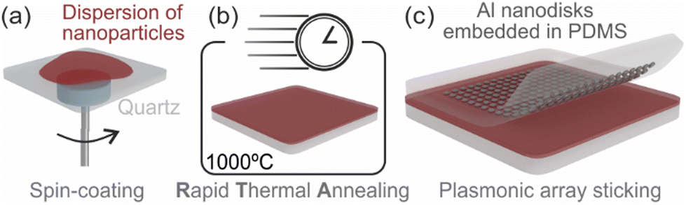 | ||
| Fig. 1 Scheme of the experimental procedure. (a) Spin-coating deposition of the phosphor nanoparticles. (b) Rapid thermal annealing (RTA) of the samples. (c) Placement of the plasmonic sticker on the film processed by RTA. | ||
We prepare transparent nanophosphor layers from alcoholic dispersions of GdVO4:Eu3+ nanoparticles by spin coating over quartz substrates.6 It is well known that photophysical and structural properties of phosphors materials are closely related. In this context, thermal processing is key in order to increase the brightness of RE-doped crystals, which turns out to be particularly critical for nanophosphors. We compare the structural properties of films annealed at 1000 °C using a conventional oven (heating rate of 1 °C per minute) and RTA (10 °C per second). Scanning electron microscopy (SEM) images – see Fig. 2a–c show that conventional processing leads to uncontrolled crystal growth and the emergence of cracks when films are annealed at 1000 °C – see Fig. 2b, as it has been reported for nanophosphor films of similar composition.8 In stark contrast, RTA roughly preserves the morphology of the thin film, as displayed in Fig. 2c. Atomic force microscopy (AFM) measurements reveal that the mean square average of height profile deviations (rms) turns out to be 27 nm for as-deposited films. This value increases up to 79 nm when conventional annealing is performed. Interestingly, short thermal processing limits grain growth, preserving the surface roughness of the films (rms = 25 nm, see ESI†), which prevents transparency loss. X-ray diffraction analysis (Fig. 2d) shows that annealed samples feature improved crystallinity: the intensity of the reflections increases and their full width at half maximum reduces with the thermal processing (see ESI†). As a matter of fact, crystallite size increases from 31 nm for as-prepared films to 45 nm and 68 nm for films annealed at 1000 °C using high and slow heating rates, respectively. Hence, conventional thermal processing brings to light a trade-off between transparency and efficiency in nanophosphor thin films. Fig. 1e shows the zeroth-order transmittance (T) for as-deposited samples and samples annealed at 1000 °C. As-deposited films are highly transparent, with values of transmittance around 90%. Conventional annealing reduces T drastically due to a significant increase of light scattering associated. In contrast, films remain highly transparent (>80%) when processed by RTA, since fast thermal processing does not yield rougher films. Notice that T reduction in this case cannot be only associated to diffuse scattering but rather to an increase in the specular reflectance due to a higher refractive index, which increases from 1.30 to 1.66 at λ = 600 nm when films are annealed by RTA. Indeed, a close inspection of the films reveals certain densification in the layer. In fact, this is further confirmed by estimating the layer thickness of films annealed from their optical response, which reduces from ∼250 nm to ∼190 nm after RTA processing.
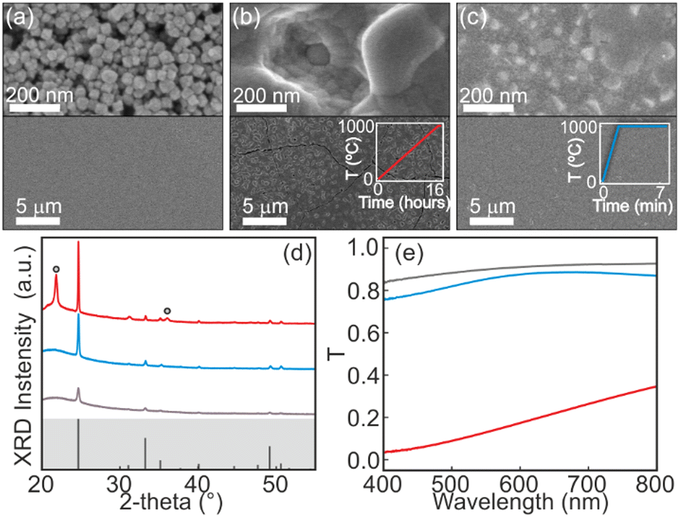 | ||
| Fig. 2 (a–c) Scanning electron micrographs of the top view of GdVO4:Eu3+ nanophosphor films as-deposited (a), and annealed at 1000 °C in a conventional oven (b) or using RTA (c). Insets show time profiles of the thermal processing. (d) X-ray diffraction patterns of samples as-deposited (grey), annealed at 1000 °C in a conventional oven (red) and 1000 °C with RTA (blue). Diffractogram of standard PDF-86-0996 (ICDD 2014) is also shown as grey lines for comparison. Circles highlight reflections associated to cristobalite structure. (e) Zeroth-order transmittance for light incident in a close-to-normal direction for as-deposited nanophosphor films (grey), and films annealed at 1000 °C in a conventional oven (red) or using RTA (blue). | ||
We performed static and dynamic PL measurements. Fig. 3a shows PL intensity curves together with a picture of a nanophosphor layer heated up to 1000 °C with RTA upon UV excitation. Red conversion associated to the main emission band of Eu3+ is clearly observed, which corresponds to the transition 5D0 → 7F2. As-deposited samples exhibit absolute PLQY below 8%. Besides, it is worth mentioning that as-prepared samples feature a certain lack of stability due to V5+ to V4+ reduction upon photoexcitation with ultraviolet light since such reduction leads to the formation of oxygen vacancies that act as quenchers of the emission.26 Thermal processing yields higher values of the PLQY. In particular, we measure 67% for samples annealed in the conventional oven and 82% using RTA, which indicates that slow annealing at such high temperatures induces structural changes that are detrimental for the emission. Notice that although non-transparent films result slightly brighter, which we attribute to the effect of the scattering that may affect both light absorption of the pump and outcoupling of the emitted light, PL intensity increases drastically with the thermal processing regardless of the heating rate compared to as-prepared films. Finally, time-dependent PL was monitored at λ = 620 nm, as displayed in Fig. 3b. Fittings of the experimental data using a two exponential model are also plotted. Values of the resulting lifetimes are listed the ESI.† Results for as-deposited films show a short decay component (0.31 ms, 22%), typically associated to cations that sit on the surface of the nanophosphor, and a long decay component (0.92 ms, 78%), associated to Eu3+ located in the bulk of the nanoparticle. Thermal processing yields an increase in the short component due to defect removal (0.37 ms, 9%), along with a reduction of the long one, which we attribute to the increase in the refractive index of the layers due to film densification (0.82 ms, 91%). Besides, the relative fraction of the short component diminishes (from 22% to 9%) since the size of nanocrystals grow as a result of thermal processing, reducing the surface to volume ratio of the nanoparticles. Besides, our measurements confirm that slow annealing at high temperature induces structural changes that compromise the photophysical properties of the films. Indeed, conventional heating results in lower average lifetime and PLQY values compared to those attained for RTA at the same temperature.
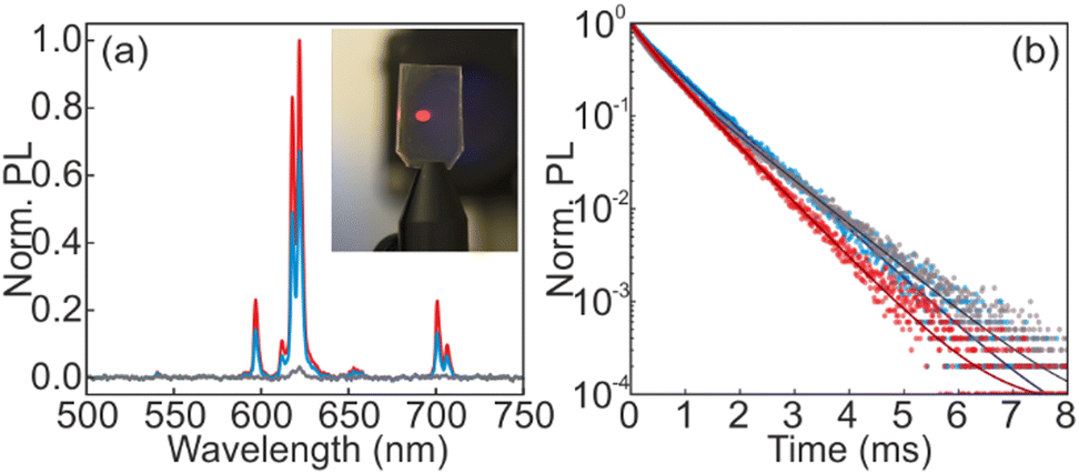 | ||
| Fig. 3 (a) Normalized photoluminescence (PL) of GdVO4:Eu3+ films as-deposited (grey), and annealed at 1000 °C in a conventional oven (red), or using RTA (blue). Inset shows the red emission of the film annealed at 1000 °C with RTA upon excitation with a 285 nm LED. (b) Time-dependent PL of the same films. Fitting curves to a double exponential model are also shown as black lines. | ||
We marriage our films processed by RTA with arrays of aluminium nanodisks embedded in a flexible poly(dimethyl)siloxane (PDMS) layer. It is noteworthy that scattering in films processed by conventional annealing prevents such combination, as shown in the ESI.† Details regarding the fabrication of the antenna array can be found in the ESI† section and have been reported elsewhere.27 The plasmonic arrays consist of aluminium disks arranged on a square array with a lattice parameter of 380 nm, 50 nm-height and 230 nm-diameter. The spectroscopic response of such sticker placed atop our nanophosphor film annealed at 1000 °C by RTA is shown in Fig. 4a and b. First, we measure the angular dependence of the optical extinction of the system – see Fig. 4a, defined as 1 − T/T0 where T is normalised to that of the reference film devoid the plasmonic sticker (T0). Three bands of high extinction can be distinguished at normal incidence, as shown in Fig. 4b. Specifically, we observe two barely dispersive broad bands of high extinction centred around 570 nm and 679 nm, which are associated to the excitation of localized surface plasmon resonances (LSPRs) in the aluminium nanodisks. The extinction map also shows a narrow mode at 597 nm, whose spectral position clearly changes with the angle of incidence. Indeed, such narrow feature is the fingerprint of a surface lattice resonance (SLR), which is a collective mode that emerges as a result of the diffractive coupling between different LSPRs in the array, as simulations confirm (see ESI†). For this reason, they appear at frequencies close to the Rayleigh Anomalies (RAs), i.e. the condition under which light is diffracted in the plane of the array. We fit the spectral position of the RA at normal incidence and plot the dispersion of (±1, 0) and (0, ±1) with white dashed lines in Fig. 4a to demonstrate that the dispersion of SLRs follow that of the RAs. Notice that the effective index of the collective mode (1.55) takes a value that is between the index of the nanophosphor film (1.66) and that of the PDMS sticker (1.43). Fig. 4b also displays the extinction spectrum at an incident angle of 5°, where the SLR associated to (1,0) diffracted order shifts from 597 nm at normal incidence to 620 nm. As a result, SLRs spectrally overlap with the main emission bands of Eu3+ nanophosphors. The hybrid plasmonic–photonic character of SLRs mediate the decay of excited emitters and its efficient radiation to free space, which provides effective control over the spontaneous emission. Fig. 4b displays the corresponding PL spectra at 0° and 5° normalized to the maximum PL intensity of a reference film. As a result, we observe a directional enhancement of the PL. Angular emission profiles are shown in the ESI.† In particular, we observe a 3.0-fold emission enhancement for the 580 nm band at 0° and a 2.8-fold at 620 nm for light collected at 5°. Notice that only SLRs induce PL enhancement. In contrast, the localized character of the broad resonance centred at 679 nm barely influences RE luminescence. To further investigate the angular dependence of the emission, we employ Fourier microscopy. The angular distribution of light reflected by the samples around 620 nm is displayed in Fig. 4c for both the reference (left semicircle) and the plasmonic system (right semicircle). Notice that the reference was measured from the sticker in a region without metallic nanoparticles. The coupling of the incident light to SLRs supported by the array gives rise to narrow bands of low reflection that follow the dispersion of the RAs of (±1,0) and (0, ±1) diffracted orders, as displayed in Fig. 4c. The angular dependence of the PL intensity is shown in Fig. 4d. The emission pattern of the flat nanophosphor film does not show any directional feature, as expected from a random distribution of emitters that behave as a Lambertian source. In turn, the plasmonic array yields a specific directional response of the emission of nanophosphors with bands of enhanced PL associated to SLRs, i.e. bright bands that follow the dispersion of RAs. In particular, a 5-fold PL directional enhancement of light extracted from the nanophosphor film is observed in a direction close to the normal to the surface. Notice that bands of high PL intensity are superimposed to a background that is slightly brighter than the reference due to a combination of scattering of the pump and enhanced outcoupling. Finally, it is worth to mention that PL enhancement values shown in Fig. 4b and d deviate slightly. We attribute such differences to the way in which the system is excited in each experiment, which result in a different contribution of the pump to the enhancement. Finite Difference Time Domain (FDTD) simulations shown in the ESI† provide insight into the physical origin of the emission enhancement described and the collective character of the mode observed at 590 nm correspond to the excitation of a SLR that yields a field enhancement that extends away of the aluminium nanodisks in the volume occupied by the nanophosphors.
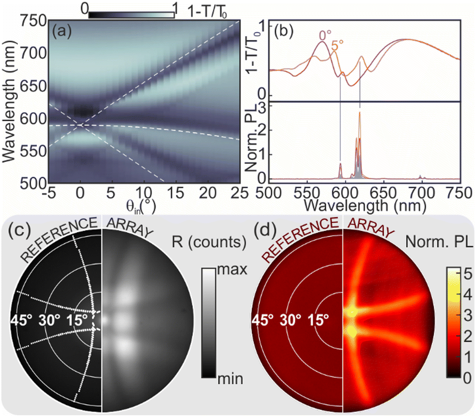 | ||
| Fig. 4 (a) Angular dependence of the extinction spectra measured from the nanophosphor film coated with the plasmonic sticker. (b) Extinction spectra (top) at 0° (purple) and 5° (orange). Rayleigh anomalies (RAs) of (±1, 0) and (0, ±1) diffracted orders are also shown as dashed white lines. Photoluminescence (PL) intensity spectra (bottom) collected from the nanophosphor film coated with the plasmonic sticker at 0° (purple) and 5° (orange). PL of a reference film is also shown for comparison (shaded grey curve). All spectra are normalized to the maximum intensity of the reference. (c and d) Fourier image of the reflectivity (c) and PL (d) at 620 nm of the nanophosphor film coated with the plasmonic sticker (right semicircle) and that of the reference film (left semicircle). RAs of (±1, 0) diffracted orders are also shown as dashed white lines. Values are normalized to the maximum intensity measured for the reference. | ||
In conclusion, we have demonstrated a novel method to perform ultrafast thermal processing of transparent nanophosphor thin films using rapid thermal annealing. Heating ramps as fast as 10 °C per second allow improving the crystallinity of the lattice, reducing defects and increasing the photoluminescence quantum yield of the films above 80% without inducing grain size grow, and thus, without compromising the transparency of the coatings. Then, we combine nanophosphor films processed this way at temperatures as high as 1000 °C with periodic arrays of metal nanodisks that support plasmonic resonances. As result, we show that large area plasmonic arrays embedded in flexible stickers strongly shape the directionality of the emission of transparent thin nanophosphor films. We have proven a 5-fold enhanced emission in specific directions that are given by the periodicity of the array. This directional enhancement originates from the coupling between light emitted by the nanophosphors and collective plasmonic resonances that result from the interaction of localized surface plasmon polaritons and diffraction in the periodic array. Our results open the door to the processing of rare-earth emitting coatings that are both efficient and transparent of interest for the development a new generation of colour-converting films to be applied in lamps, displays, solar cells, markers or anti-counterfeiting systems.
Data for this paper are available at Digital CSIC at http://hdl.handle.net/10261/285609. The code for estimating the optical constants of an arbitrary layered optical material may be found at https://github.com/Multifunctional-Optical-Materials-Group.
This project has received funding from the European Research Council (ERC) under the European Union's Horizon 2020 Research and Innovation Programme (NANOPHOM, grant agreement no. 715832). E. C. O. acknowledges the grant FPU19/00346 funded by MCIN/AEI/10.13039/501100011033 and ESF Investing in your Future. S. M. and K. T. thanks support from MEXT, Japan (Kakenhi 21H04619, 22H01776, 22K18884) and the Futaba foundation.
Conflicts of interest
There are no conflicts to declare.References
- S. Pimputkar, et al. , Nat. Photonics, 2009, 3, 180 CrossRef.
- J. Y. Tsao, et al. , Adv. Opt. Mater., 2014, 2, 809 CrossRef.
- P. M. Pattison, et al. , Nature, 2018, 563, 493 CrossRef PubMed.
- Y. Zhuo and J. Brgoch, J. Phys. Chem. Lett., 2021, 12, 764 CrossRef CAS PubMed.
- K. Panigrahi and A. Nag, J. Phys. Chem. C, 2022, 126, 8553 CrossRef CAS.
- D. Geng, et al. , ACS Appl. Mater. Interfaces, 2019, 11, 4219 CrossRef CAS PubMed.
- N. O. Núñez, et al. , Dalton Trans., 2013, 42, 10725 RSC.
- D. Geng, et al. , Adv. Opt. Mater., 2017, 5, 1700099 CrossRef.
- L. Xu, et al. , Nanotechnology, 2019, 30, 435703 CrossRef CAS.
- D. Hebbar, et al. , Mater. Res. Bull., 2019, 119, 110544 CrossRef.
- D. Hebbar, et al. , New J. Chem., 2022, 46, 7032 RSC.
- W. Skorupa, et al. , Surf. Coat. Technol., 2017, 314, 169 CrossRef CAS.
- A. F. Koenderink, et al. , Science, 2015, 348, 516 CrossRef CAS PubMed.
- J. F. Galisteo-López and G. Lozano, J. Appl. Phys., 2021, 130, 200901 CrossRef.
- S. Zou, et al. , J. Chem. Phys., 2004, 120, 10871 CrossRef PubMed.
- V. G. Kravets, et al. , Phys. Rev. Lett., 2008, 101, 087403 CrossRef PubMed.
- B. Auguié and W. L. Barnes, Phys. Rev. Lett., 2008, 101, 14390 CrossRef PubMed.
- Y. Chu, et al. , Appl. Phys. Lett., 2008, 93, 181108 CrossRef.
- G. Lozano, et al. , Light: Sci. Appl., 2016, 5, e16080 CrossRef PubMed.
- G. Lozano, et al. , Light: Sci. Appl., 2013, 2, e66 CrossRef.
- G. Lozano, et al. , Nanoscale, 2014, 6, 9223 RSC.
- M. Ramezani, et al. , Phys. Rev. B, 2016, 94, 125406 CrossRef.
- L. Langguth, et al. , ACS Nano, 2013, 7, 8840 CrossRef CAS PubMed.
- S. R. K. Rodriguez, et al. , Appl. Phys. Lett., 2012, 100, 111103 CrossRef.
- S. Murai, et al. , APL Photonics, 2017, 2, 026104 CrossRef.
- T. Muto, et al. , ECS Trans., 2009, 16, 135 CrossRef CAS.
- K. Agata, et al. , Appl. Phys. Lett., 2021, 118, 021110 CrossRef CAS.
Footnote |
| † Electronic supplementary information (ESI) available: Materials and methods; AFM images, time-dependent photoluminescence analysis; extinction measurements; angular emission profiles; FDTD simulations. See DOI: https://doi.org/10.1039/d2cc04779a |
| This journal is © The Royal Society of Chemistry 2023 |