
 Open Access Article
 This Open Access Article is licensed under a Creative Commons Attribution-Non Commercial 3.0 Unported Licence
Multi-feature round silicon membrane filters enable fractionation and analysis of small micro- and nanoplastics with Raman spectroscopy and nano-FTIR†
Michaela
Meyns
 a,
Frank
Dietz
b,
Carin-Sonja
Weinhold
b,
Heiko
Züge
b,
Saskia
Finckh‡
a and
Gunnar
Gerdts
*a
a,
Frank
Dietz
b,
Carin-Sonja
Weinhold
b,
Heiko
Züge
b,
Saskia
Finckh‡
a and
Gunnar
Gerdts
*a
aAlfred-Wegener-Institute, Helmholtz Centre for Polar and Marine Research, Heligoland, Germany. E-mail: gunnar.gerdts@awi.de
bFraunhofer Institute for Silicon Technology ISIT, Itzehoe, Germany
First published on 23rd December 2022
Abstract
Visualization of small micro-(20–1 μm) and nanoplastics (<1 μm) combined with chemical identification is still a challenge. To address this, we designed and manufactured easy-to-handle silicon membrane filters with a standard round filter geometry of 25 mm in diameter and a 10 mm diameter filtration area, holding hexagonal sections with periodically arranged pores of either 250 nm or 1 μm. Due to their flat and reflective surface, the filters serve as a versatile substrate for spectroscopic identification of particles. Optical markers at different levels of magnification, including the bare eye, allow for an easy transfer and repositioning of samples between instruments and methods as well as for a re-measurement of nanoscale particles. We demonstrate how nanoscale particles of weakly absorbing polymers such as polyethylene and polystyrene are analyzed on these filters by nano-FTIR, a combination of atomic force microscopy and Fourier transform infrared spectroscopy. By sequential filtration we separated the fractions of small micro and nanoplastics from a degraded polylactic acid coffee cup lid and achieved subsequent identification by Raman and nano-FTIR spectroscopy. The applications presented in this study will enable future research regarding the identification of small polymer particles difficult to access by other methods.
Introduction
Small micro- (SMPs, 20–1 μm) and nanoplastics (NPs, <1 μm)1,2 with their impact on ecosystems and toxicological effects on organisms are currently subjects of concern and intense research. However, complex challenges still exist for qualitative and quantitative analysis of these particles in the environment.3,4 To advance in this direction, several analytical challenges need to be addressed from sample preparation to reliable identification and sizing of SMPs and NPs. For extended reviews on the growing field of SMP and NP analysis, we would like to point to ref. 3–5.A key technique for identifying microplastic (MP) particles is microspectroscopy based on infrared (IR) or Raman radiation.4 At the macroscopic scale, IR- and Raman spectroscopy are often seen as complementary in their results. Molecular vibrations may be active towards one but not the other, as the underlying physical processes differ. Towards smaller sample sizes, Fourier transform infrared microspectroscopy (μ-FTIR) is capable of identifying MPs down to 11 μm in size when combined with an FPA detector.6 Raman microspectroscopy, Raman imaging and surface enhanced resonance spectroscopy have reached the nanoscale in terms of particle size, with 50 to 200 nm particles detected in liquids7,8 and 30 nm to 1 μm particles, bare or aggregated with plasmonic Ag particles on a dry substrate.9–15 Correlative application of scanning electron microscopy (SEM) and Raman is among the candidates for conjugated methods that may provide more holistic data for samples containing SMPs and NPs with nanoscale resolution.3,4,11,17,18 Nevertheless, the laser excitation, for example, at 532 nm applied in Raman spectroscopy can bring along problems such as burning of particles and fluorescence.11,19 IR-spectroscopy requires longer, less energetic IR excitation wavelengths and is thus not affected by fluorescence and more benign towards the sample integrity. The latter is a desired feature for fundamental and analytical studies as it allows for re-analysis of specific particles with the same or other analytical methods afterwards. To reach a resolution in the range of SMPs and NPs, IR-spectroscopy can be combined with scanning probe techniques to offer an alternative to current methods.
Nano-FTIR is an s-SNOM (scanning near-field optical microscopy) derived method combining the resolution of atomic force microscopy with chemical analysis by IR-spectroscopy. It is based on light scattering from a tip operated in tapping mode (unlike AFM-IR, which is conducted in contact mode). The lateral resolution in spectroscopy depends on the diameter of the needle-like cantilever probe and reaches down to approximately 20 nm.20 Spectroscopic IR-features have already been recorded for polymethylmethacrylate (PMMA) particles down to 37 nm in diameter.21 Due to its high resolution as well as the possibility of destruction- and label-free analysis, the method has been applied in a wide range of studies related to polymers and sensitive biological materials. Examples are the characterization of thin films and blends,22,23 single type and core–shell polymer nanoparticles,21,24 multilayer structures,25 phospholipid membranes and the distribution of cholesterol within them as well as viruses.21,26–28 Nano-FTIR spectra comply well with references from macroscopic IR-techniques and are thus suited for library-based identification.20,23,27,29
Methodological and theoretical details of scattering-type scanning near field optical microscopy (s-SNOM) and nano-FTIR are explained in ref. 20 and 30–32. Parameters relevant for this study are the following. With the probe in tapping mode at frequency Ω, the IR-beam generated for example from a broadband mid-IR laser is focused on the tip of the probe. The tip and the sample interact relative to their distance d, with near-field effects occurring at a closer distance to the surface. The interaction is controlled by the wavenumber-dependent dielectric function ε(ω) of the materials, which also determines local absorption and reflection properties.20,31,33 The ratio of incoming and scattered light at the tip is given by the complex valued scattering coefficient σ(ω) = sn(ω)eiφn(ω) with NF-amplitude sn (OnA) and NF-phase φn (OnP). Scattered light is recorded using an asymmetric Michelson interferometer and a mid-IR detector. To obtain the nano-FTIR absorption an (ω) of the sample, the data are normalized to a reference, typically recorded on a clean reflective surface such as a silicon (Si) wafer. It is given by the imaginary part (Imag.) of the Fourier transformed, complex valued and normalized near-field spectrum an(ω) = Im[σ(ω)] = s(ω)sin[φn(ω)].20,27,29
A correlation of absorption and tapping distance is taken into account by demodulating the detector signal at different harmonic orders n of the tapping frequency Ω. With higher orders, there is less background signal and more influence of near-field interactions, while the penetration depth decreases.34 A unique feature of this technique is thus its ability to provide data from different probing depths within one measurement due to simultaneous demodulation of the detector signal at different n. For nano-FTIR and s-SNOM, both surface-sensitive techniques, probing depths of up to 100 nm below the surface were reported.25,35,36
Apart from spectroscopic analysis, probe-based methods provide topographic scans with three dimensional particle sizes and data derived from the interaction between the tips and the surface, such as mechanical phase scans. In total, nano-FTIR and s-SNOM offer the possibility of nanoscale particle-based microscopy and identification on the one hand and additional characterization for understanding fundamental properties such as depth-related surface modifications on the other. In order to take full advantage of these options, the substrate on which the samples are dried before analysis must fulfill certain requirements.
The first one concerns the visibility and delicacy of the sample. SMPs and NPs are not visible to the eye. To spot them and possibly be able to re-locate them on a substrate, they must stick out from the background and some type of visual orientation is necessary. This requires regular structures on a flat substrate and optical guides at different levels of magnification. Due to their size, they also exhibit altered properties for example in terms of density-related behaviour and are especially intricate analytes. They require even stronger contamination control than microplastics. As they should be transferred and disturbed as little as possible once dried, it is important to work with easy-to-handle but highly defined filters that can be integrated into standard sequential filtration and purification processes and that may also act as substrates during analytical measurements. Second, the substrate itself should not exhibit a strong absorption pattern in the relevant spectral region (here 1800–1070 cm−1) and must be reflective for nano-FTIR measurements.37 Third, being a scanning probe method in tapping mode at a constant tip–sample distance, nano-FTIR requires a clean, well-distributed and not too polydisperse sample. Dried organic residues or salts may affect the attraction between the tip and the sample, reduce reflection or in the worst case contaminate the tip. The possibility to thoroughly rinse a sample without losing particles is thus of utmost advantage. Particles larger than 1 μm in between nanoscale particles may induce crashes, as the feedback loop controlling the distance between the tip and the sample may not respond quickly enough. Such a problem may be omitted by collecting the larger fraction on a prior filter and analysing it separately.
Ideal filters thus combine a flat surface, defined and ordered pores and optical neutrality in the IR-region with mechanical and chemical resistance.
In recent literature on SMP and NP particle identification, several basic types of substrates other than flat surfaces are applied. Metal, mostly gold, coated membrane filters are commercially available with typical pore diameters of 0.4 or 0.2 μm from several providers, while alumina-coated membranes are rather custom made.38 Both types lack ordered pore distribution and orientation marks. The same is true for filter substrates prepared by deposition of SERS-active silver nanowires on filter paper.16
Substrates with ordered micro- and nanoscale cavities are intended to both fix the particles in position and increase recorded Raman signals by formation of hot spots.9,39 The impermeability of such structures as well as a tendency of aggregate formation between several particles smaller than the cavity were seen as problematic for our purpose.
Silicon (Si) filters prepared by lithographic methods on the other hand are obvious candidates. Some examples with ordered pores of 10 μm were already applied in the analysis of MPs.19,40 However, filters with smaller pore sizes than 1 μm and standard round filter dimensions are currently not commercially available. Using a silicone seal as an adapter that also tapers the glass filtration funnel on the top side of the filter as in ref. 40 is not an option with nano-FTIR, as silicones may release compounds such as polydimethylsiloxane (PDMS), which we observed to interfere with measurements in another context.
For this reason, we developed Si membrane round filters with two pore sizes (250 nm and 1 μm) and multiple features that facilitate analysis and intermethod transfer for small particle fractions with minimum disturbance of the delicate samples. In the following examples, we are thus able to take full advantage of advanced microscopy methods such as nano-FTIR for detection and identification of SMPs and NPs.
Experimental
Particles
“Non-functionalized” PS spheres with 194 nm diameter and plum purple stained PS spheres (360, 420) with an average diameter of 530 nm in aqueous solution (2% solids content) were purchased from Bangs Laboratories. PE spheres of 200 to 9900 nm were obtained as a powder from Cospheric and used without further purification. PMMA particles with 189 nm in diameter and a PDI of 0.124 in water were provided by Agnes Weimer, Universität Hamburg. PS and PMMA particles were purified by ultracentrifugation prior to sample preparation and finally dispersed in pure ethanol (ROTISOLV HPLC Gradient Grade 99.9%, Carl Roth). For further details, see the ESI.† In the case of a mixed PS and PMMA sample, 125 μL of purified PS and 150 μL of purified PMMA dispersions in ethanol were mixed and diluted to 2 mL with pure ethanol. A small pipette tip of PE was dispersed in pure ethanol by five two-second intervals of dipping into a Bandelin Sonorex Rk100, 35 kHz, 80/320 W ultrasound bath (see Fig. S1†). The dispersion was diluted until it was almost optically clear.For PLA coffee lid degradation, four 1 cm2 pieces were cut out of the coffee cup lid, put into a Duran glass bottle of 50 mL capacity and left in 75% ethanol (pure ethanol diluted with ultrapure water, Milli-Q, 18 MΩ) for two minutes for sterilization. After removing the ethanol and rinsing with freshly poured ultrapure water, the pieces were covered with 20 mL ultrapure water. The bottle was closed with alumina foil and heated to 70 °C in a water bath for four days,41 afterwards the solution was left to stand in the dark at room temperature for further 78 days.
Single and sequential filtration: for trials with natural samples such as Arctic snow and ice from sets earlier analysed for MPs,42,43 2 to 5 mL of untreated samples were filtered with 250 nm pore diameter Si membrane filters after passing 2 mL of freshly poured ultrapure water through the filtration set-up with a glass funnel. An under pressure of less than −10 mbar was applied with a membrane pump. For sterilization, 5 mL of 75% ethanol, diluted from pure ethanol, was added without letting the funnel run dry. In the case of PLA lid particles, two filters with 1000 and 250 nm pores were stacked in the filtration set-up visible in Fig. 4 and S2,† separated by 5 mm with a Teflon ring. The sample solution was sonicated for 30 s in 2 s intervals. At −50 mbar, 2 mL of ultrapure water was added before 5 mL of sample solution was filtered. The residual sample was removed from the space between filters by slowly increasing the under pressure to −200 mbar.
All glassware and tweezers were thoroughly rinsed with water and ethanol after use and wiped with ethanol-drenched cotton wool where applicable to remove particulate contaminants prior to overnight soaking in an Edisonite super bath (Schülke). After rinsing with filtered tap water and fresh ultrapure water (Milli-Q), the pieces were left to dry inside the clean bench.
Si membrane filters
Si membrane filters were produced from 725 μm thick, 3 ohm cm−1 Boron p-doped 8′′ Si wafers, semi-standard, purchased from Active Business GmbH. For details of the process, see Fig. 1e and the ESI.†Sample analysis and data treatment
Scanning electron microscopy (SEM) analysis of Si membrane filters was carried out on a Zeiss CB 1540EsB. Dimensions on the wafers were measured with a Hitachi 9260A critical dimension SEM. The bow over the wafer was measured using a Bruker Profilometer Dektak XT.Atomic force microscopy and nano-FTIR spectroscopy were carried out on a NeaSNOM by neaspec. The spectroscopy unit was equipped with a mid-IR super continuum laser with five excitation ranges between 2200 and 610 cm−1 and an asymmetric Michelson Interferometer with a total interferometer distance of 800 μm. The laser provides an output of around 1 mW for the final spectra between 2000 and 670 cm−1 and bandwidths of 700–800 cm−1. Standard settings for spectroscopy were an interferometer distance of 500 μm, an optical resolution of 10 cm−1, 1024 pixels per interferogram, an integration time of 15 ms per pixel and an average of 32 scans or 4 separate measurements with 8 scans. The set point was 80%, and the tapping amplitude was between 70 and 80 nm in the approached state. The interferometer was set to the white light position and the spectral range was 2000–1000 cm−1 for scans including optical data. The probes were metal-coated, arrow-shaped neaspec spectroscopy tips with resonance frequencies of 244–266 kHz and tip diameters of approximately 20 nm for particle spectroscopy. A NanoWorld Arrow-NCPt, with a resonance frequency of 285 kHz was applied in scans of substrates without the sample. After each measurement, the obtained spectra were normalized to a reference measured on an empty spot on the filter, preferably next to the respective particle.
Standard nano-FTIR data treatment involved phase-offsetting and averaging of four scans with eight runs (in total 32 scans averaged) with neaPLOT software and smoothing by a 9-point moving average. Where necessary, a phase tilt correction was applied in combination with phase offsetting. Baseline subtraction as for the PE spectrum in Fig. 3 was conducted with the asymmetric least squares method for data between 1800 and 1300 cm−1 and thresholds set to 0.05 for PS and 0.02 for PMMA. In the case of plum purple PS beads spectra of two ranges were combined manually, phase corrected and smoothed by a 9-point moving averaging. Scan data were levelled, shifted and plotted with Gwyddion 2.50, which was also employed to determine particle heights from profiles.
ATR-IR reference spectra of purified particle samples measured in bulk and the initial PLA lid were recorded on a Bruker Tensor spectrometer with an ATR unit in the wavenumber range of 4000–400 cm−1 with an aperture of 6 mm, a resolution of 4 cm−1 and 32 scans.
Raman spectra were obtained on a rap. i.d. Bioparticle Explorer equipped with a 100× objective. Laser excitation was set to 532 nm, at an exposure time of 15 seconds, 13% laser power (2.6 mW) and an optical resolution of 8 cm−1. A reference of the PLA lid was measured on a Witec Alpha 300R microscope with an excitation wavelength of 532 nm, laser power of 24 mW and a G2 grating with 600 g mm−1 and BLZ = 500 nm.
Plum purple stained PS particles were analysed with a Zeiss Axio Imager at a magnification of 20× in bright field mode and with an excitation of 385 nm at 21% intensity from the attached Calibri LED source for fluorescence microscopy. The applied filter was HECFP/YPF/mcherry. Both images were overlapped to create the image shown.
Results and discussion
Si membrane filters
Flat and reflective surfaces are a prerequisite in microscopy and especially scattering techniques. For nanoscale particles, surface roughness and localizability of the particles are another important factor.To account for these necessities, we designed and produced Si membrane filters with two pore sizes of 250 nm and 1 μm from Si wafers by multiple steps including lithography. Their design allows handling them in the same way as conventional membrane filters, in addition to higher mechanical and chemical stability and low optical interference in the IR-region. In contrast to rectangular Si filters, no adapters are needed when utilizing standard glass filtration set-ups.40 With a diameter of 25 mm, a filtration area of 10 mm in diameter and a maximum thickness of 350 μm (Fig. 1a), these filters fit into typical holders and are mechanically more stable than other equivalents with nanoscale pores such as polycarbonate membranes. As the filters are produced within the original wafer structure, each is held in the framework using the four remaining Si-bridges (Fig. S3e†). After sawing, there are four flat sections at the rims of each filter, where the diameter is reduced to 24.57 mm. This does not disturb handling or filtration and is even an advantage for aligning the sample in its holder for measurements. Two marks top and left on the outside of the filtration area guide the eye to the correct orientation of the sample.
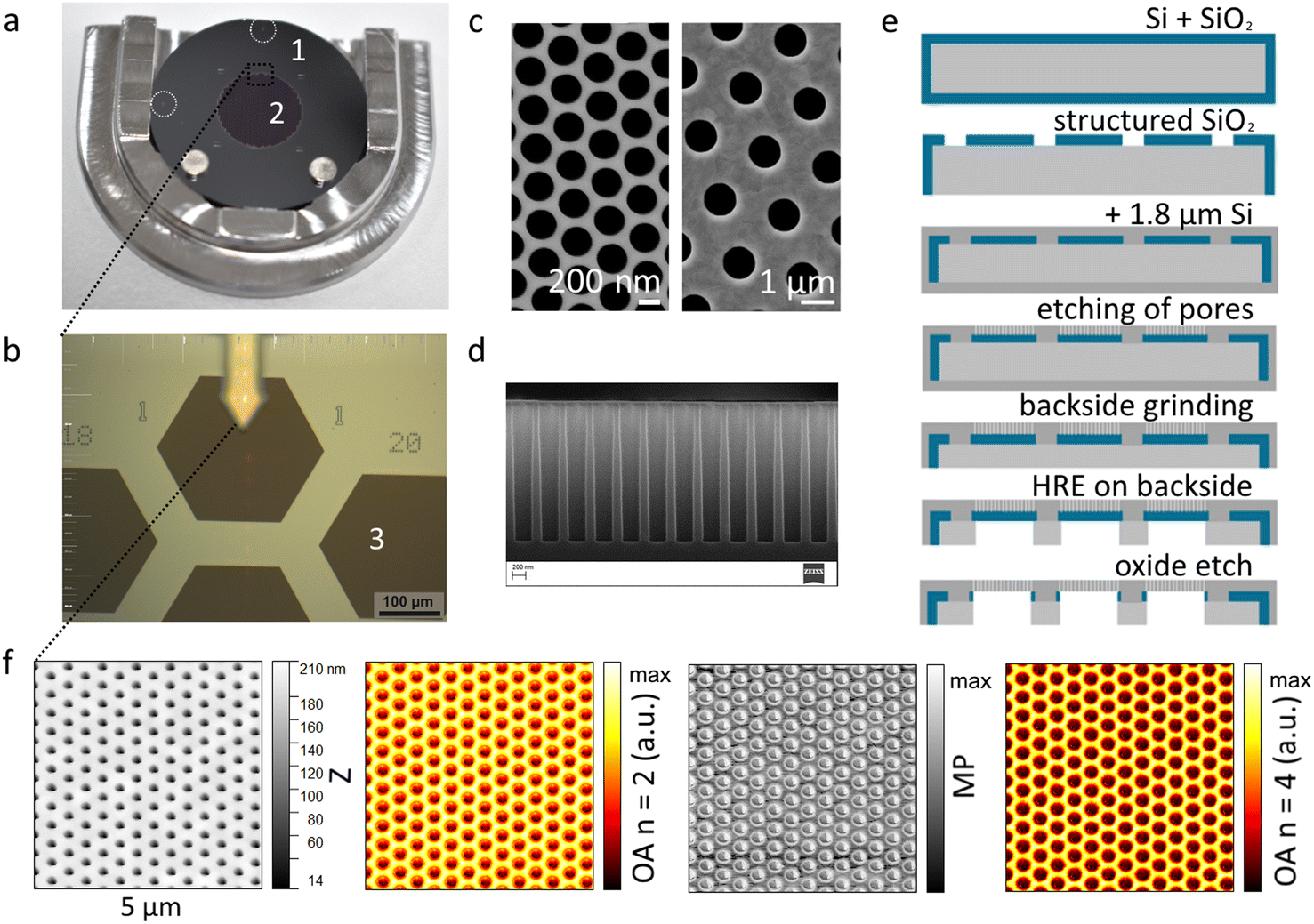 | ||
| Fig. 1 (a) Si membrane filters with optical guides for manual alignment (inside white circles), and a custom-made sample holder with four marks for automated positioning for Raman micro- and nano-FTIR spectroscopy. Magnets may be added to keep the sample in place. (b) Top and center hexagons with coordinates (x, y: 19, 1). Numbers surrounding the hexagonal pore areas of the outer ring facilitate orientation on the sample and manual re-location of specific spots. White numbers in (a) and (b) indicate (1): Si membrane filter, (2): filtration area, (3): pore area. (c) Scanning electron micrograph of different filter devices with pore areas containing pores of 250 nm and 1 μm in diameter. (d) Cross section of pore geometry with 250 nm diameter pores. (e) Scheme of steps and key elements in the production process of the filter. HRE: high resolution etching. (f) Comparison of the topographical scan (height z), n = 2 deconvolution of the optical amplitude measured with white light settings for radiation in the range 2000–1000 cm−1, the mechanical phase signal (MP) and the n = 4 optical amplitude signal. | ||
The filters are easily handled with tweezers without affecting the filtration area and do not bend like, for example, polycarbonate (PC) membranes. In conventional polymer membrane filters with nanoscale pores, such as PC membranes, pores are distributed irregularly, while porous inorganic silver or Al2O3 filters (Anodisc) may additionally exhibit a relatively high surface roughness (Fig. S4 and S5†). Similar to the flat surfaces of Si wafers or gold-coated Si wafers, orientation on those filters is tricky, even more so for finding small particles. Revisiting specific nanoscale particles is time-consuming or impossible. With a regular distribution of pores in a structured pattern, irregularities are quickly spotted.
Key to reaching small but ordered pores was the design of the filtration area. A pattern of stabilizing elements supports a total of 931 hexagonal pore sections in a honeycomb structure (Fig. 1b). The hexagonal filter areas are easily recognizable at 20× magnification and assigned to a honeycomb coordinate system with x and y origins on the top left (Fig. S3†). This facilitates returning to specific spots on the sample, especially since hexagons in the outmost ring are identified by dotted x- and solid y-coordinates. Numbering follows practical aspects evaluated from manual positioning and orientation at 20-fold magnification, allowing for movement along horizontal and vertical lines within the coordinate system. During production, four positioning marks for automated orientation are introduced in a square pattern around the filtration area (Fig. S3†). Even though automated recognition is not yet available with our nano-FTIR instrument, these marks may serve such purposes for other present or future methodologies.
Clogging of filters is a frequent problem with nanoscale fractions, often due to adsorption of even smaller compounds. Additionally, nano-FTIR can be sensitive to IR-active residues on the surface, while possibly picking up sticky compounds with the probing tip. To avoid these effects, we chose a minimum feasible pitch of 400 nm between hexagonally distributed 250 nm pores (Fig. 1c), leading to a pore area of 12% inside the filtration area. For the larger 1 μm pores, the pitch was set to 2 μm, also resulting in a pore area contribution of 12%. This way, no large amounts of contamination can remain on the surface and particles tend to lock into separated positions on the holes. This is an advantage with small spheres, as they may be moved by interaction with the tip on flat surfaces or form large aggregates within drying patterns on flat surfaces.
The membrane filters were produced by a sequence of steps to structure front and back sides (Fig. 1e). The filter fabrication starts with a deposition of SiO2 on 8-inch Si-wafers. Afterwards, the filtration area with the coordinate system was realized by structuring the oxide. Then, a 1.8 μm thick amorphous Si layer was deposited for the pore areas. After performing lithography on a DUV scanner, the pores were structured with a modified Bosch etching process (for the difference before and after modification, see Fig. S7†). In this process, etching and polymer deposition happen in turns to achieve straight pore walls over the entire 1.8 μm without significantly widening the desired diameter (Fig. 1d).
During resist development and production of the 250 nm design, the average hole diameter on a wafer varies from 230 nm to 280 nm. Hole diameters within a filtration area vary by about ±20 nm. The 1 μm design shows less variation. This can be improved by optimizing the process sequence.
Through lithography using an MA200 Mask Aligner the backside was structured up to the filter stack creating the hexagonal support structure. Furthermore, the circular outline with small bridges between the filters was prepared (Fig. S3†). Only in the last steps, the filters were separated from the original 8-inch wafer by sawing the remaining Si-bridges. Finally, the protection layer was removed and the filters were cleaned. Additionally a descum process with plasma-induced oxygen radicals was performed, producing a nanometre thin oxide layer with higher hydrophilicity. To achieve stable and flat filters with a minimum bow, stress optimization was necessary.44 An initial positive deflection of at least 6300 nm within the hexagons was reduced to below 80 nm over a distance of 230![[thin space (1/6-em)]](https://www.rsc.org/images/entities/char_2009.gif) 000 nm (Fig. S6†), or a height difference of 1 nm along a distance of 2875 nm.
000 nm (Fig. S6†), or a height difference of 1 nm along a distance of 2875 nm.
Final Si membrane filters are slightly hydrophilic as they are shortly treated with oxygen plasma in the last step of their fabrication, yielding a layer of oxide comparable to native oxide (up to 2 nm). A minimum under pressure is enough to start the filtration. However, the filters withstood under pressures of −800 mbar and over pressures of several bar.
For stable and oriented positioning as well as transferability between the applied NeaSNOM nano-FTIR and rap. i.d. Raman microspectroscopy units, we developed a stainless steel sample holder with an asymmetric geometry to fit into both set-ups (Fig. 1a).
Fig. 1f depicts the 5 × 5 μm scans derived from trace signals of the height (Z), and the local near-field reflection/optical amplitude (n = 2 and 4), resulting from broadband IR-irradiation, as well as the mechanical phase scan. Stronger similarities appear between scans with height and demodulation of the optical signal at the second order of the tapping frequency, while the mechanical phase and the optical signal demodulated at a higher order resemble each other more closely. The reason behind this is that the first two are more prone to interactions with larger areas of the tip or larger electromagnetic fields around the tip, while the latter two more strongly reflect the interaction between the bottom of the tip and the sample. This agrees with more confined electric field distributions at an oscillating metallic tip of a near-field microscope at higher orders, as mapped from data of Fourier demodulation analysis.45 Comparability of the lateral resolution with SEM, however, generally depends on the diameter and geometry of the probe tip. The tips for nano-FTIR are metal-coated, with tip diameters of approximately 20 nm or more, compromising either resolution or signal intensity, depending on the sample and the aim.
Nano-FTIR spectroscopy of nanoscale polymer particles
A mixture of purified nanoscale PMMA and PS particles with average diameters 189 and 194 nm suspended in 99.9% ethanol was deposited on Si membrane filters with 250 nm pores by filtration at −20 mbar. In Fig. 2a three distinct particles and dimers are visible in the local reflection in the form of 2D optical amplitude data. The strongest reflection occurs on the flat parts of the membrane, while it is substantially weaker where particles absorb the IR-light. No puddles of organic residues, such as surfactants that may hamper analysis or contaminate the tip are visible, which emphasizes the advantage of a sieve-like substrate over flat surfaces or wells where residues may accumulate. With a clean surface, it is possible to measure reference spectra in close proximity to the particles in the course of nano-FTIR measurements. This way, reference measurements may be conducted frequently without having to move to an external Si reference wafer, if concerns of tip contamination or changes in the background signal arise. In the case of severe contamination or damage, there will be no proper spectrum, as the interaction between the tip and the sample is disturbed. | ||
| Fig. 2 (a) Nano-FTIR/s-SNOM scan of local white light reflection with incident radiation of 2000–1000 cm−1 (n = 2). (b) 3D topography with measured particle heights of (1): 150 nm, (2): 140 nm and (3): 185 nm. (c) Nano-FTIR point spectra with n = 2 recorded as 32 averages with an integration time of 10 ms per pixel identify PS (1) and PMMA (2 and 3). | ||
The 3D projection of the scan not only illustrates the difference in the particle height, which is more accurate as it is less affected by the geometry of the probing tip than is the lateral expansion, but also clarifies a dimeric structure of the smaller particles visible in the scan. The spectroscopic signal is obtained by demodulation of the nano-FTIR interferograms recorded on top of the particles under identical settings. A range of 1800 and 1300 cm−1 is well suited for differentiating between standard polymers.23 Not only do the resulting spectra confirm a tendency of higher intensity with larger size and therefore the thickness for PMMA,21,46,47 but they also illustrate the difference in signal intensity between PMMA and PS within this spectral region as observed in polymer films.23 ATR-FTIR reference spectra of dried particle samples are available in the ESI.† These results promise the feasibility of future automation. At the state of the art technology of the applied instrument, automation is not yet feasible as it is not possible to move the stage to fixed positions in an automated sequence. With further advancement and accompanying software adaptation, this will likely be possible, as the sample stage may already be controlled through software and is movable in 3 dimensions. An automated approach of the sample towards the tip is implemented. To account for future automation with nano-FTIR or automated analyses with other techniques such as Raman or fluorescence mapping methods, we included markers on the membranes that are detectable both by eye and by a machine. This allows future users to employ automated techniques for positioning in their instrument.
Micro to nano scale with complementing methods
Due to the orientation aids on the filter, it is facile to revisit and measure an identical set of particles on different days by removing the sample from the set-up in between. This allows an exchange of probing tips for scans and nano-FTIR or a transfer between different analytical methods. Fluorescent nanoscale polymer particles, for example, not only serve as model particles in uptake or recovery studies but are also highly useful in terms of process control when handling NPs. They are detected either by nano-FTIR where visible fluorescence does not interfere, or by fluorescence microscopy as described in the ESI.† Different size ranges or properties of a collected sample containing SMP and NP are accessible by a combination of Raman microspectroscopy and nano-FTIR, with pore sizes of the filters determining the lower size limit.Fig. 3a shows a sample of standard polyethylene (PE) particles (cospheric, 200–9900 nm) at 20-fold magnification in the top camera of the nano-FTIR set-up. The sample was deposited from pure ethanol on a membrane filter with pore sizes of 250 nm at a slight under pressure. The marked region is magnified with a 100× objective in (b) with a 5 μm particle in its centre. Raman spectroscopy with a green laser emitting at 532 nm results in clear spectra of the particle in the range of 3240 to 570 cm−1. Data below 570 cm−1 were cut off due to the high intensity Si–Si peak at 520 cm−1. For full spectra see the ESI.† A wider 2nd order Si–Si signal is visible below 1000 cm−1. However, a well-identifiable polymer spectrum of PE is obtained. After transferring the sample and re-locating the hexagon, a scan within the nearfield microscope reveals a nanoscale particle barely visible before. Nano-FTIR spectra of the particle were recorded with low intensity incident radiation of 2000–1000 cm−1 with 940 μW under ambient conditions at a resolution of 10 cm−1. Interactions with water vapour are the reason for a noisier background compared to the ATR-IR reference after smoothing by a 9-point moving average. However, the C–H peak at 1466 cm−1 corresponds well between an ATR-IR reference measurement of the dried batch sample and the nano-FTIR spectra demodulated at n = 2 or 3 of the tapping frequency. The n = 2 signal carries more background information, for example on scattering processes, while higher orders contain more information from the surface of a particle. Unwanted background scattering can be removed by baseline correction, for example applying an asymmetric least squares method as for the corrected n = 2 spectrum in Fig. 3e. In the higher, n = 3 order spectrum, a CO-peak is distinguishable at 1721 cm−1, same as that in the ATR-IR reference. This was also observed for other particles in the sample. Spectra demodulated at n = 4 are not always showing clear peaks. However, in cases with a clear CO-peak it was there even stronger compared to the main C–H-deformation peak, indicating that the surface of the particles is at least partially oxidized. Notably, such penetration depth-related information is obtained from one single set of scans, as all orders are demodulated simultaneously from the obtained interferogram. Core–shell structures and layer thicknesses may be investigated further by specialized analyses.34 If the analytical goal is single particle identification based on the core material, under the chosen parameters the n = 2 spectrum appears more suited as there is less interference of possible surface oxidation.48
 | ||
| Fig. 3 (a) PE micro- and nanobeads on a Si membrane filter examined with (b) a 100× optical objective and (c) Raman spectroscopy with 532 nm incident radiation for a 5 μm particle, data are normalized to 1 within the window and (d) atomic force microscopy coupled with (e) IR-spectroscopy including asymmetric interferometric detection for nano-FTIR. In (e) spectra of the ATR-IR reference of the same batch of PE beads and nano-FTIR spectra with different demodulation orders are scaled and offset for clarity. Nano-FTIR spectra of the single particle were recorded under ambient conditions with the reference recorded directly on the membrane next to it. Data were treated as detailed in the Methods section. | ||
Sequential filtration
Biodegradable and other plastics slowly disintegrate in water, releasing small particles and other compounds.49–51 To demonstrate the ease of separating the small fractions and directly applying the Si membrane filters as substrates for spectroscopic analysis, we exemplarily chose to thermally disintegrate a biodegradable coffee cup lid made of polylactic acid (PLA) in ultrapure water. For temperatures above 60 °C, a phase change towards higher crystallinity was reported for PLA, accompanied by hydrolysis and the formation of nanoscale particles.41 For this reason, small 1 × 1 cm2 pieces of the lid were heated to 70 °C in ultrapure water for four days in a water bath and stored at room temperature for 78 days. Two fractions were collected by sequential filtration over pore sizes of 1 μm and 250 nm. This was carried out with a typical set-up for microplastic sample filtration with a glass funnel and a stainless steel filter table save for a Teflon ring with a thickness of 5 mm to separate the filters (see the photo in Fig. 4). Before adding the sample solution, the setup was filled with 2 mL of fresh ultrapure water to fill gaps and avoid stronger disturbances during filtration. After filtration of the sample at −50 mbar more water was passed to remove possible molecular residues. The larger fraction was analysed with Raman microspectroscopy, and the smaller one with nano-FTIR. Fig. 4 summarizes the findings and shows a clean separation of the two fractions. There is a clear correlation between the measured particle and the reference spectra. This underlines that the combination of a Si membrane filter with standard measures and nanoscale pore sizes with micro- and nano spectroscopy is able to both provide size information and chemical identity and even additional information such as 3D geometry for the SMP and NP fractions.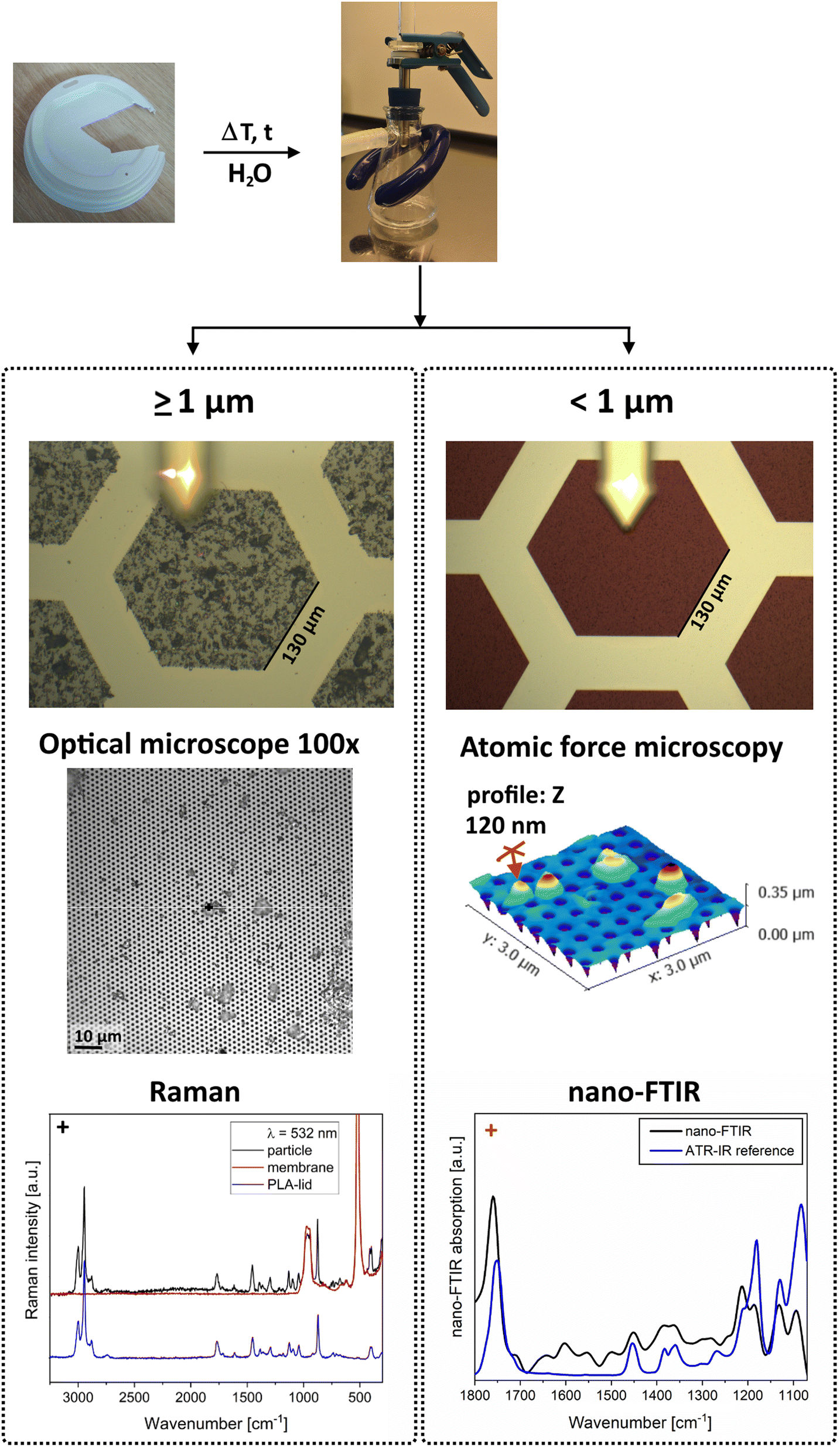 | ||
| Fig. 4 Pieces of a PLA coffee lid in ultrapure water were heated to 70 °C for 4 days and stored for 28 days before a sequential filtration on 1 μm and 250 nm pore membranes. Light microscope images and a topographic scan of the smaller fraction show the well-distributed sample. Raman and nano-FTIR spectra of 4 μm- and 120 nm-sized particles correlate well with the reference spectra of the initial lid material. | ||
Future challenges
Probe-based techniques provide a variety of information; however, their high sensitivity leads to special requirements regarding the purification of samples to be analysed for the presence of SMPs and NPs. Inorganic and organic residues may contaminate the cantilever tip and prevent successful spectroscopy. In samples from “fairly clean” arctic snow and ice such SiO2-based fragments and components with typical amide bands between 1700 and 1500 cm−1 (see Fig. 5) prolong analysis. In a millilitre of water from the Northern Sea, for example, there are on average 106 Bacteria per mL and 107 viruses per mL during summer.52 Both count towards the marine colloidal fraction and need to be removed from samples together with other non-plastics in order to reduce the natural sample load. This should happen without creating new and smaller residues inside the sample that may themselves disturb analysis (e.g., iron-based nanoparticles in a misbalanced Fenton reaction). | ||
| Fig. 5 (a) Optical scan and (b) nano-FTIR spectra of a typical, naturally occurring component in marine samples: SiO2-based fragments with strong bands around 1100 cm−1 and residues containing amide-groups with characteristic bands between 1700 and 1500 cm−1, for example from proteins. (c) Size ranges of contents in natural marine samples. | ||
Among the remaining challenges for NP analysis in general, the largest one is clearly to obtain purified and concentrated samples.11 They should still be representative of the initial sample, while extracting and up-concentrating polymer particles without affecting their shape or material. Multi-featured membrane filters may thus play a vital role in future progress of SMP and NP analysis.
Conclusions
By choosing a design with hexagonal support structures, we were able to produce standard-sized 25 mm diameter Si membrane filters with a filtration area of 10 mm in diameter containing regularly distributed 250 nm and 1 μm pores. These filters directly serve for sequential filtration of the SMP and NP fractions as well as their subsequent spectroscopic analysis, as demonstrated with a degraded PLA coffee lid material. Combined with the mechanical advantage of silicon over polymer membrane filters, Si round filters offer the opportunity to be implemented into existing MP processing, for example, as an additional filtration step.With optical guides for sample positioning and numbering of the hexagons as well as an ordered pore distribution, facile location and revisiting of spots and specific particles are equally convenient as transfers between different microscopes.
The produced membranes present a significant step in introducing nano-FTIR as an additional method for examining NPs. They help to pin NPs to their position during scanning probe analysis and allow for substantial removal of residues from samples that may hamper spectroscopy otherwise. This way, not only particle size and identity in the form of IR-spectra are accessible but also three-dimensional profiles, depth-related differences in the material composition and local reflection as well as local absorption data of the scanned sample.
Si membrane filters contain optical markers for visual and future automated orientation on the sample. By depositing further, for example metallic, layers, their optical properties may be adapted to suit different analytical methods and alter the pore size. Combined with their robust design, the filters will allow for increased spectroscopic reproducibility, intermethod comparisons and improved QA/QC processes.
In combination with nano-FTIR or other methods, Si membrane filters provide ample options for better understanding the state, behaviour and distribution of small plastics in the environment.
Conflicts of interest
There are no conflicts to declare.Acknowledgements
We would like to thank Johannes Lemburg and the technical workshops at AWI Helgoland and Bremerhaven for fabricating and developing custom parts, Yasin Durmaz (Ludwig Maximilian University of Munich) and neaspec for discussions and nano-FTIR support, Medina Veliu for experimental help with membrane testing, Hannah Jebens for experimental help and ATR-spectra, Sebastian Primpke for Raman reference data and Agnes Weimer, Universität Hamburg, for providing PMMA particles. Additionally, we would like to thank the frontend lithography team and the backend wet-chemistry team at ISIT, especially Uwe Ziller, Didem Öztürk and Beate Engel. The work was funded through the project “Size is important” (FIT12317001) by the WTSH Business Development and Technology Transfer Corporation of Schleswig Holstein. We acknowledge support by the Open Access Publication Funds of Alfred-Wegener-Institut Helmholtz-Zentrum für Polar- und Meeresforschung.References
- N. B. Hartmann, T. Huffer, R. C. Thompson, M. Hassellov, A. Verschoor, A. E. Daugaard, S. Rist, T. Karlsson, N. Brennholt, M. Cole, M. P. Herrling, M. C. Hess, N. P. Ivleva, A. L. Lusher and M. Wagner, Environ. Sci. Technol., 2019, 53, 1039–1047 CrossRef CAS PubMed.
- J. Gigault, A. T. Halle, M. Baudrimont, P. Y. Pascal, F. Gauffre, T. L. Phi, H. El Hadri, B. Grassl and S. Reynaud, Environ. Pollut., 2018, 235, 1030–1034 CrossRef CAS PubMed.
- N. P. Ivleva, Chem. Rev., 2021, 121, 11886–11936 CrossRef CAS PubMed.
- S. Primpke, S. H. Christiansen, W. Cowger, H. De Frond, A. Deshpande, M. Fischer, E. B. Holland, M. Meyns, B. A. O'Donnell, B. E. Ossmann, M. Pittroff, G. Sarau, B. M. Scholz-Bottcher and K. J. Wiggin, Appl. Spectrosc., 2020, 74, 1012–1047 CrossRef CAS PubMed.
- J. Delgado-Gallardo, G. L. Sullivan, P. Esteban, Z. Wang, O. Arar, Z. Li, T. M. Watson and S. Sarp, ACS ES&T Water, 2021, 1, 748–764 Search PubMed.
- L. Cabernard, L. Roscher, C. Lorenz, G. Gerdts and S. Primpke, Environ. Sci. Technol., 2018, 52, 13279–13288 CrossRef CAS PubMed.
- R. Gillibert, G. Balakrishnan, Q. Deshoules, M. Tardivel, A. Magazzu, M. G. Donato, O. M. Marago, M. Lamy de La Chapelle, F. Colas, F. Lagarde and P. G. Gucciardi, Environ. Sci. Technol., 2019, 53, 9003–9013 CrossRef CAS PubMed.
- C. Schwaferts, V. Sogne, R. Welz, F. Meier, T. Klein, R. Niessner, M. Elsner and N. P. Ivleva, Anal. Chem., 2020, 92, 5813–5820 CrossRef CAS PubMed.
- A. Valsesia, M. Quarato, J. Ponti, F. Fumagalli, D. Gilliland and P. Colpo, Sci. Rep., 2021, 11, 362 CrossRef CAS PubMed.
- B. E. Ossmann, G. Sarau, H. Holtmannspotter, M. Pischetsrieder, S. H. Christiansen and W. Dicke, Water Res., 2018, 141, 307–316 CrossRef CAS PubMed.
- R. Schmidt, M. Nachtnebel, M. Dienstleder, S. Mertschnigg, H. Schroettner, A. Zankel, M. Poteser, H. P. Hutter, W. Eppel and H. Fitzek, Micron, 2021, 144, 103034 CrossRef CAS PubMed.
- Z. Sobhani, X. Zhang, C. Gibson, R. Naidu, M. Megharaj and C. Fang, Water Res., 2020, 174, 115658 CrossRef CAS PubMed.
- C. Fang, Z. Sobhani, X. Zhang, C. T. Gibson, Y. Tang and R. Naidu, Water Res., 2020, 183, 116046 CrossRef CAS PubMed.
- C. Fang, Z. Sobhani, X. Zhang, L. McCourt, B. Routley, C. T. Gibson and R. Naidu, Water Res., 2021, 194, 116913 CrossRef CAS PubMed.
- X.-X. Zhou, R. Liu, L.-T. Hao and J.-F. Liu, Talanta, 2021, 221, 121552 CrossRef CAS PubMed.
- Q. Yang, S. Zhang, J. Su, S. Li, X. Lv, J. Chen, Y. Lai and J. Zhan, Environ. Sci. Technol., 2022, 56, 10818–10828 CrossRef CAS PubMed.
- G. Sarau, L. Kling, B. E. Ossmann, A. K. Unger, F. Vogler and S. H. Christiansen, Appl. Spectrosc., 2020, 74, 1155–1160 CrossRef CAS PubMed.
- G. Li, Z. Yang, Z. Pei, Y. Li, R. Yang, Y. Liang, Q. Zhang and G. Jiang, Talanta, 2022, 249, 123701 CrossRef CAS PubMed.
- A. Käppler, D. Fischer, S. Oberbeckmann, G. Schernewski, M. Labrenz, K. J. Eichhorn and B. Voit, Anal. Bioanal. Chem., 2016, 408, 8377–8391 CrossRef PubMed.
- F. Huth, A. Govyadinov, S. Amarie, W. Nuansing, F. Keilmann and R. Hillenbrand, Nano Lett., 2012, 12, 3973–3978 CrossRef CAS PubMed.
- M. Brehm, T. Taubner, R. Hillenbrand and F. Keilmann, Nano Lett., 2006, 6, 1307–1310 CrossRef CAS PubMed.
- M. Breuer, M. Handloser and T. Gokus, Photonics Spectra, 2018, https://www.photonics.com/Articles/Nano-FTIR_Spectroscopy_Reveals_Materials_True/a63044 Search PubMed.
- M. Meyns, S. Primpke and G. Gerdts, Anal. Methods, 2019, 11, 5195–5202 RSC.
- M. Goikoetxea, I. Amenabar, S. Chimenti, M. Paulis, J. R. Leiza and R. Hillenbrand, Macromolecules, 2021, 54, 995–1005 CrossRef CAS.
- L. Mester, A. A. Govyadinov, S. Chen, M. Goikoetxea and R. Hillenbrand, Nat. Commun., 2020, 11, 3359 CrossRef CAS PubMed.
- A. M. Siddiquee, A. Houri, K. A. Messalea, J. Lin, T. Daeneke, B. Abbey, A. Mechler and S. Kou, J. Phys. Chem. Lett., 2020, 11, 9476–9484 CrossRef CAS PubMed.
- A. Cernescu, M. Szuwarzynski, U. Kwolek, P. Wydro, M. Kepczynski, S. Zapotoczny, M. Nowakowska and L. Quaroni, Anal. Chem., 2018, 90, 10179–10186 CrossRef CAS PubMed.
- I. Amenabar, S. Poly, W. Nuansing, E. H. Hubrich, A. A. Govyadinov, F. Huth, R. Krutokhvostov, L. Zhang, M. Knez, J. Heberle, A. M. Bittner and R. Hillenbrand, Nat. Commun., 2013, 4, 2890 CrossRef PubMed.
- A. A. Govyadinov, I. Amenabar, F. Huth, P. S. Carney and R. Hillenbrand, J. Phys. Chem. Lett., 2013, 4, 1526–1531 CrossRef CAS PubMed.
- F. Keilmann and R. Hillenbrand, Philos. Trans. R. Soc., A, 2004, 362, 787–805 CrossRef CAS PubMed.
- T. Taubner, R. Hillenbrand and F. Keilmann, Appl. Phys. Lett., 2004, 85, 5064–5066 CrossRef CAS.
- N. Ocelic, A. Huber and R. Hillenbrand, Appl. Phys. Lett., 2006, 89, 101124 CrossRef.
- R. Hillenbrand and F. Keilmann, Phys. Rev. Lett., 2000, 85, 3029–3032 CrossRef CAS PubMed.
- A. A. Govyadinov, S. Mastel, F. Golmar, A. Chuvilin, P. S. Carney and R. Hillenbrand, ACS Nano, 2014, 8, 6911–6921 CrossRef CAS PubMed.
- T. Taubner, F. Keilmann and R. Hillenbrand, Opt. Express, 2005, 13, 8893–8899 CrossRef CAS PubMed.
- R. Krutokhvostov, A. A. Govyadinov, J. M. Stiegler, F. Huth, A. Chuvilin, P. S. Carney and R. Hillenbrand, Opt. Express, 2012, 20, 593–600 CrossRef PubMed.
- M. Autore, L. Mester, M. Goikoetxea and R. Hillenbrand, Nano Lett., 2019, 19, 8066–8073 CrossRef CAS PubMed.
- B. E. Oßmann, G. Sarau, S. W. Schmitt, H. Holtmannspotter, M. Pischetsrieder, S. H. Christiansen and W. Dicke, Anal. Bioanal. Chem., 2017, 409, 4099–4109 CrossRef PubMed.
- G. Xu, H. Cheng, R. Jones, Y. Feng, K. Gong, K. Li, X. Fang, M. A. Tahir, V. Kolev Valev and L. Zhang, Environ. Sci. Technol., 2020, 54, 15594–15603 CrossRef CAS PubMed.
- A. Käppler, F. Windrich, M. G. Loder, M. Malanin, D. Fischer, M. Labrenz, K. J. Eichhorn and B. Voit, Anal. Bioanal. Chem., 2015, 407, 6791–6801 CrossRef PubMed.
- H. Xu, X. Yang, L. Xie and M. Hakkarainen, Biomacromolecules, 2016, 17, 985–995 CrossRef CAS PubMed.
- I. Peeken, S. Primpke, B. Beyer, J. Gutermann, C. Katlein, T. Krumpen, M. Bergmann, L. Hehemann and G. Gerdts, Nat. Commun., 2018, 9, 1505 CrossRef PubMed.
- M. Bergmann, S. Mutzel, S. Primpke, M. B. Tekman, J. Trachsel and G. Gerdts, Sci. Adv., 2019, 5, eaax1157 CrossRef CAS PubMed.
- P. Temple-Boyer, E. Scheid, G. Faugere and B. Rousset, Thin Solid Films, 1997, 310, 234–237 CrossRef CAS.
- F. Mooshammer, M. A. Huber, F. Sandner, M. Plankl, M. Zizlsperger and R. Huber, ACS Photonics, 2020, 7, 344–351 CrossRef CAS.
- S. Mastel, A. A. Govyadinov, T. V. A. G. de Oliveira, I. Amenabar and R. Hillenbrand, Appl. Phys. Lett., 2015, 106, 023113 CrossRef.
- J. Aizpurua, T. Taubner, F. J. Garcia de Abajo, M. Brehm and R. Hillenbrand, Opt. Express, 2008, 16, 1529–1545 CrossRef PubMed.
- L. Rowenczyk, A. Dazzi, A. Deniset-Besseau, V. Beltran, D. Goudouneche, P. Wong-Wah-Chung, O. Boyron, M. George, P. Fabre, C. Roux, A. F. Mingotaud and A. T. Halle, Environ. Sci. Technol., 2020, 54, 4102–4109 CrossRef CAS PubMed.
- W. Zhang, Z. Dong, L. Zhu, Y. Hou and Y. Qiu, ACS Nano, 2020, 14, 7920–7926 CrossRef CAS PubMed.
- B. Gewert, M. M. Plassmann and M. MacLeod, Environ. Sci.: Processes Impacts, 2015, 17, 1513–1521 RSC.
- H. P. H. Arp, D. Kuhnel, C. Rummel, M. MacLeod, A. Potthoff, S. Reichelt, E. Rojo-Nieto, M. Schmitt-Jansen, J. Sonnenberg, E. Toorman and A. Jahnke, Environ. Sci. Technol., 2021, 55, 7246–7255 CrossRef CAS PubMed.
- G. Gerdts, A. Wichels, H. Döpke, K.-W. Klings, W. Gunkel and C. Schütt, Helgol. Mar. Res., 2004, 58, 230–242 CrossRef.
Footnotes |
| † Electronic supplementary information (ESI) available: (1) Further experimental details, photos and drawings of Si membrane filters, the sample holder, micrographs and AFM-scans, bow measurement over the membrane area, SEM-micrographs of cross sections after Bosch etching procedures, ATR-IR spectra of purified particles measured in bulk, full Raman spectra of the PE particle on Si membrane filter, micrographs and the nano-FTIR spectrum with optical scan of a fluorescent PS particle. (2) Txt file with ATR-IR spectra of purified and dried PS and PE particles. Other spectra are available from the authors. See DOI: https://doi.org/10.1039/d2ay01036d |
| ‡ Current address: UFZ Helmholtzzentrum für Umweltforschung, Leipzig, Germany |
| This journal is © The Royal Society of Chemistry 2023 |