A high-performance terahertz absorber based on synthetic-patterned vanadium dioxide metamaterials
Received
6th August 2022
, Accepted 7th November 2022
First published on 1st December 2022
Abstract
In this work, we designed a terahertz absorber based on vanadium dioxide (VO2) with tunable and ultra-broadband characteristics. This absorber is composed of four identical synthetic VO2 patterns, a dielectric layer and a metal reflector layer from top to bottom. The designed absorber is found to achieve essentially total reflection when VO2 is in the insulated state. The designed absorber has an absorption bandwidth of over 90% absorptance up to 7.7 THz in the frequency range of 5.36–13.06 THz when VO2 is in the metallic state. By adjusting the conductivity of VO2, the absorber realizes near-perfect modulation of the amplitude with its absorbance dynamically tuned from 4.31% to 100%. The operating principle of the ultra-broadband absorber is interpreted by wave interference theory, impedance matching theory, and electric field analysis. Compared to previously reported terahertz absorbers, the designed absorber offers significant improvements in the absorption broadband, and it also has many advantages such as a simple structure, polarization insensitivity, and a flexible incident angle. These tunable ultra-broadband terahertz absorbers hold great promise in the fields of photochemical energy absorption, thermal emitters, and stealth devices.
Introduction
In the past few decades, terahertz waves have attracted great research interest because of their huge scientific value and promising applications in fields such as detection technology,1 wireless communication2 and medical imaging.3 However, since most natural materials only have a weak electromagnetic response to a terahertz wave, there is a so-called “terahertz gap” that limits the further development of terahertz technology.4 Fortunately, the emergence of metamaterials has effectively solved this problem to some extent. Metamaterials are a new class of artificial synthetic materials composed of periodic subwavelength metals or dielectrics arranged in accordance with certain rules.5–9 Due to their extraordinary electromagnetic response characteristics, they can produce a resonance effect with electromagnetic waves in a specific frequency band. Therefore, metamaterials have been widely used in stealth devices,10 sensors,11 communication devices,12,13 and imaging devices14 in recent years. Functional devices such as absorbers,15–17 filters,18 and modulators19,20 based on metamaterials have also been proposed. Among them, terahertz absorbers have become a research hotspot in recent years, and significant progress has been made in thermal emitters,21 detectors,22,23 and solar absorbers.24 Landy et al. first proposed a perfect metamaterial absorber coupled with electromagnetic fields at narrow frequencies to absorb incident light by independently manipulating electrical resonance and magnetic resonance.25 Since then, the research results of metamaterial absorbers have continued to grow vigorously, but they faced troubles caused by fixed operating frequencies and narrow operating bandwidths. Even if stacked multi-layer structures or resonant structures of multiple sizes are used in the same plane to increase the bandwidth, they also bring about the problems of complex structures and difficult fabrication.26–28 As a result, numerous researchers are devoted to looking for metamaterial absorbers with tunable characteristics and broadband absorption.
In recent years, researchers have combined phase change materials such as graphene,29–32 liquid crystals,33,34 bulk Dirac semimetals35–37 and VO238–41 with metamaterial absorbers to achieve the tunable properties of absorbers. VO2 is a commonly used phase change material.42 The phase transition process can be controlled by electronic control,43 temperature control,44,45 and light control,46,47 and its resistivity changes by up to 5 orders of magnitude. VO2 is in the insulating state at room temperature and undergoes a phase change when the temperature exceeds the phase change temperature of 340 K. The lattice of VO2 transforms from a monoclinic rutile structure at low temperature to a tetragonal rutile structure at high temperature, which is externally manifested as a sudden change from the insulating phase to the metallic phase.48,49 Based on the natural tunable advantage of VO2, it can be combined with metamaterials to realize active polarization manipulation devices50 and switching devices.51 So far, some metamaterial absorbers based on VO2 to achieve tunable broadband characteristics have been reported [see ref. 45–52 in Table 1]. Although these absorbers show the advantages of an adjustable absorption amplitude and a large bandwidth in a simple manner, the absorption bandwidth and adjustable performance of current absorbers are still difficult to meet practical requirements.
Table 1 Comparison of the absorption performance of different VO2-based terahertz absorbers. (Absorbers marked with an asterisk are dual broadband absorbers)
| Ref. |
Absorption bandwidth (THz) |
Tunable range (%) |
Material |
|
52
|
0.33 |
30–100 |
VO2 |
|
53
|
0.65 |
0–100 |
VO2 and graphene |
|
54
|
0.83 |
7–90 |
VO2 and graphene |
|
55
|
1.23 |
4–100 |
VO2 |
|
56
|
1.25 |
15–96 |
VO2 |
|
57* |
2.03, 2.32 |
2–94 |
VO2 |
|
58
|
2.45 |
4–100 |
VO2 |
|
59
|
3.43 |
8–100 |
VO2 |
| This paper |
7.7 (5.36–13.06) |
4.31–100 |
VO2 |
In this paper, we presented a VO2-based tunable ultra-broadband terahertz absorber. The absorber is composed of a patterned VO2 film and a metal plate spaced by a dielectric layer. The results indicate that the absorber basically achieves total reflection, and the absorptance is nearly zero when VO2 is in the insulated state. The designed absorber has an absorption bandwidth of over 90% absorptance up to 7.7 THz in the frequency range of 5.36–13.06 THz when VO2 is in the metallic state. By altering the conductivity of VO2, the designed absorber achieves near-perfect amplitude modulation, and the absorption rate can be dynamically adjusted from 4.31% to 100%. The operating principle of the ultra-broadband absorber is explained in terms of wave interference theory, impedance matching theory, and electric field analysis. Compared with a previously reported work, the absorber has only a three-layer structure, which is easy to process and fabricate, and the absorption bandwidth is significantly improved. At the same time, the absorber also has obvious advantages, such as polarization insensitivity and a wide angle of incidence. Finally, we further investigate the effects of geometrical parameters, dielectric layer thickness, and different combinations of VO2 hybrid patterns on the absorption performance. Such tunable ultra-broadband metamaterial absorbers have important applications in the fields of optical modulators, thermal emitters, and stealth devices.
Structure design and simulation methods
A three-dimensional schematic of the overall unit structure of the ultra-broadband terahertz absorber is shown in Fig. 1. The underlying substrate of the absorber is a 1 μm-thick Au film with a conductivity of 4.56 × 10⁷ S m−1, and its thickness is much greater than the skin depth to guarantee that terahertz waves are not transmitted through. The intermediate spacer layer is SiO2 with a relative permittivity ε of 3.8, which can be regarded as a loss-free dielectric in the terahertz range.60 The VO2 synthetic pattern on the top layer is composed of four identical cross-diagonal arrows and crosses. The thicknesses of SiO2 and VO2 are h1 = 4 μm and h2 = 0.27 μm, respectively. The lattice constant of the unit cell is P = 49.5 μm. The geometrical parameters of the synthetic VO2 pattern are as follows: P1 = 20 μm, W1 = 1.95 μm, W2 = 4.4 μm, W3 = 2.1 μm, l1 = 5.6 μm, d = 4 μm, and d1 = 12 μm. Generally, the typical preparation process of the designed terahertz absorber is as follows. First, the silicon substrate is cleaned using an ultrasonic instrument. Second, a gold film with a thickness of 1 μm is plated on the silicon substrate. Next, a 4 μm thick layer of quartz is applied to the gold substrate using the ion beam method. Finally, a 0.27 μm film of VO2 is deposited on the quartz layer and the final pattern is obtained by photolithography and electron beam.
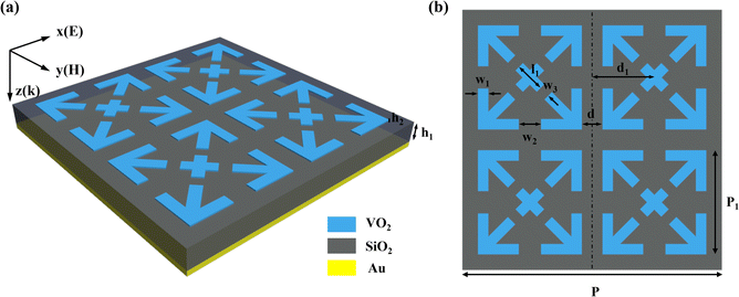 |
| | Fig. 1 (a) Schematic of the unit cell of the ultra-broadband terahertz absorber. The top layer is four identical hybrid VO2 patterns (blue), the dielectric layer is SiO2 (grey), and the bottom layer is a metal ground plate (yellow). (b) Top view of the unit cell. | |
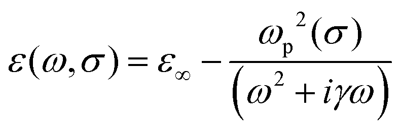
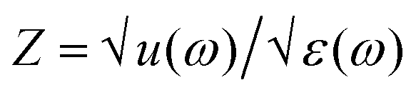
In the terahertz region, the Drude model is commonly adopted to express the optical properties of VO2,61 as illustrated in eqn (1).
| | 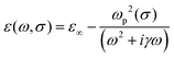 | (1) |
| | 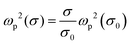 | (2) |
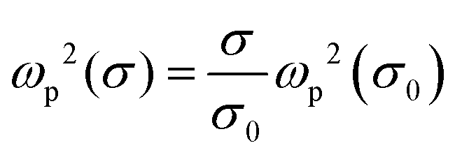
Here, the dielectric constant at high frequencies is ε∞ = 12, the collision frequency is γ = 5.75 × 10¹³ rad s−1, and the plasma frequency is ωp(σ), as shown in eqn (2). The plasma frequency is ωp(σ0) = 1.4 × 10¹⁵ rad s−1 and σ0 = 3 × 10⁵ S m−1. Here, we assume that the conductivity of VO2 in the insulating and metallic states are σ = 200 S m−1 and σ = 2 × 10¹⁵ S m−1, respectively. The finite element method in CST Microwave Studio is used to analyze the frequency domain of the designed absorber. In the CST simulation software, the X and Y directions are set as periodic boundary conditions, and the Z direction is set as open boundary conditions. According to wave interference theory, the expression of the absorption rate is obtained by A(ω) = 1 − R(ω) − T(ω). R(ω) = |S11(ω)|2 is the reflectance and T(ω) = |S21(ω)|2 is the transmittance. S11(ω) and S21(ω) can be obtained from S-parameters in CST. The underlying metal plate of the absorber is sufficient to ensure that the transmission coefficient is close to 0, that is, S21(ω) = 0. Therefore, the absorption rate can be simplified as A(ω) = 1 − R(ω).
Results and discussion
Fig. 2(a) shows the transmission, reflection, and absorption spectra of the ultra-broadband terahertz absorber from 0.1 to 15 THz at the vertical incidence of electromagnetic waves. The absorption spectra of the designed absorber are almost consistent with the transverse-electric (TE) polarization and the transverse-magnetic (TM) polarization when VO2 is in the metal state (the corresponding conductivity is σ = 2 × 10⁵ S m−1). This reflects the fact that the designed absorber is polarization-insensitive, which is mainly attributed to the rotational symmetry of the VO2 pattern. The results show that the absorption frequency with an absorption rate of greater than 0.9 is from 5.36 THz to 13.06 THz, and the realized bandwidth is 7.7 THz. The absorption spectra show four perfect absorption peaks with resonance frequencies of f1 = 7.86 THz, f2 = 9.89 THz, f3 = 11.69 THz, and f4 = 12.58 THz, which correspond to 99.9%, 99.9%, 98.4%, and 96% absorption, respectively. The center frequency of more than 90% absorption band is fc = 9.21 THz. Since the underlying metal plate is thick enough, the transmittance is zero. As shown in Fig. 2(b), we simulate the absorption rates of different polarization angles. The absorption efficiencies of TE and TM polarization waves match perfectly, and the absorption spectra do not change with the increase of the polarization angle. Therefore, the proposed ultra-broadband terahertz absorber satisfies the requirement of polarization-independent characteristics.
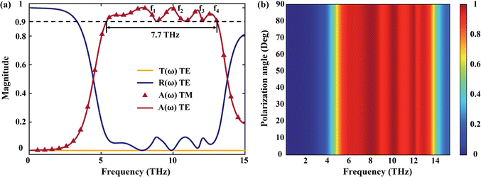 |
| | Fig. 2 (a) Transmission, reflection and absorption spectra of the ultra-broadband terahertz absorber when VO2 is in the metallic state. (b) Map of the absorption spectra at different polarization angles. | |
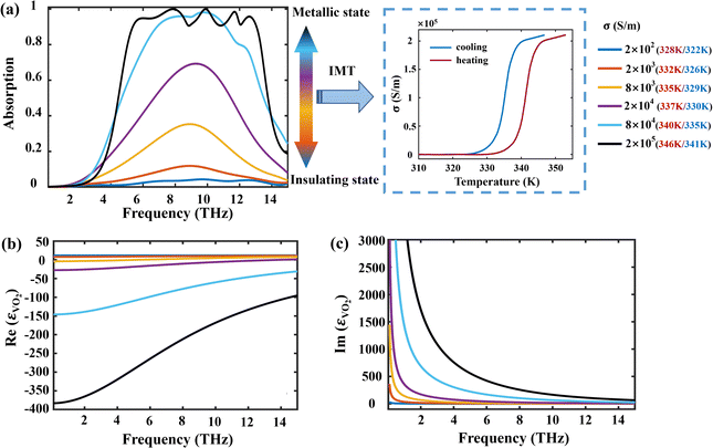
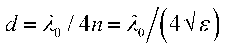
Fig. 3(a) shows the process of regulating the conductivity of VO2 by temperature and the absorption spectrum with the change of conductivity during the phase transition. The designed absorber produces an absorption peak of small amplitude with a maximum amplitude of approximately 4.31% when the conductivity of VO2 is σ = 200 S m−1, as displayed by the dark blue line in the diagram. The absorption rate of the absorber can be gradually adjusted from 4.31% to 100% when the conductivity of VO2 increases continuously from σ = 200 S m−1 to σ = 2 × 10⁵ S m−1. The insulator–metal transition (IMT) behavior of VO2 can be induced by changing the temperature (heating and cooling processes),39,62,63 as shown in the temperature–conductivity relationship on the right side of the figure. During the heating process (328–346 K), the absorption performance improves with the increasing temperature. In contrast, in the cooling process (322–341 K), the absorption reduces as the temperature decreases. The absorption effect that occurs during cooling exhibits a slight hysteresis relative to the heating process throughout the IMT process. The transition based on the crystal structure triggers different electromagnetic properties of VO2, that is, the conductivity of VO2 undergoes a variation of several orders of magnitude; thus the continuous adjustment of the absorption rate can be realized. Fig. 3(b) and (c) show the real and imaginary variation curves of the dielectric constant of VO2 at different conductivities. It can be seen from the figure that the imaginary part of the conductivity changes more obviously than the real part, and the main reasons are as follows. First, the real part of the permittivity is associated with the resonant frequency, and the imaginary part is related to the dielectric loss. Since the imaginary part of the permittivity is proportional to the conductivity, the value of the imaginary part will increase accordingly with the increase of the conductivity. Second, the central position of the absorption peak is almost unchanged, which mainly depends on the height of the intermediate spacer. According to the interference cancellation theory,64 the height of the intermediate spacer layer is determined by  (λ0 is the resonance wavelength of free space, and n and ε are the refractive index and dielectric constant of SiO2, respectively). Here, the resonance wavelength of free space is λ0 = c/fc, and the corresponding dielectric layer thickness is d ≈ 4.18 μm. In the numerical simulation, the optimized value of the actual thickness of the intermediate media compartment is h1 = 4 μm, which has a small difference with the theoretical calculation result, and the designed absorber is more in line with the interference elimination conditions.
 |
| | Fig. 3 (a) The absorption spectrum of the absorber under the normal incidence of TE polarized waves as a function of conductivity and the conductivity of VO2 as a function of temperature during the phase transition. (b and c) The real and imaginary parts of the dielectric constant with the variation of VO2 conductivity are plotted. | |
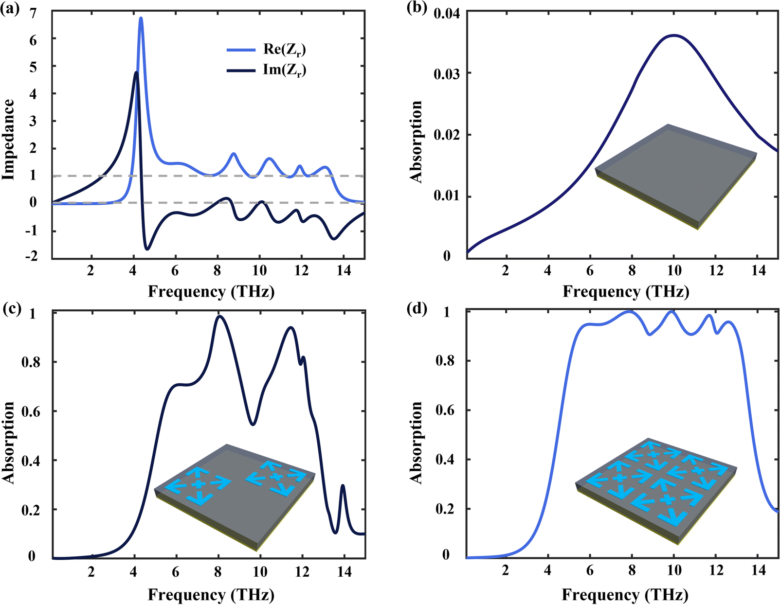
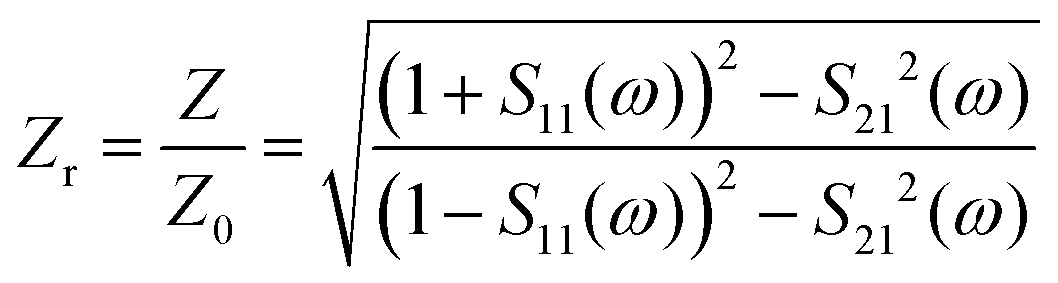
In general, impedance matching theory has been adopted to better explore the physical mechanisms of metamaterial absorbers.65,66 When the terahertz wave is incident vertically, the relative impedance between the absorber and free space is defined as follows:
| | 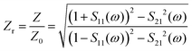 | (3) |
| | 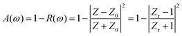 | (4) |
where

is the effective impedance of the absorber and
Z0 is the effective impedance of the free space. As shown in
Fig. 4(a), we plotted the relative impedance variation curves when the conductivity of VO
2 is 2 × 10
5 S m
−1 in the operating frequency range. It can be seen from the figure that in the frequency range from 0.1 THz to 15 THz, the real and imaginary parts of the relative impedance of the absorber tend to be 1 and 0, respectively (
i.e.,
Zr = 1). Thus, the absorption rate
A(
ω) = 1, which makes the results closer to the ideal cases. This also indicates that the effective impedance of the absorber and the impedance of the free space are matched to reach the maximum absorption bandwidth and achieve perfect absorption. In essence, the incident electromagnetic wave is continuously reflected at the upper and lower interfaces of the intermediate dielectric layer, which leads to the complete consumption of the electromagnetic energy and the confinement of the light beam in the dielectric. Additionally, we separately demonstrate the effect of hybrid VO
2 patterns on the overall absorption performance of absorbers (
e.g., unpatterned absorbers, two-patterned absorbers, and four-patterned absorbers).
Fig. 4(b) shows an unpatterned absorber consisting of only a metal ground layer and a dielectric layer. The simulation results show that the absorber produces a weak single peak with less than 3.6% absorptance. The addition of the VO
2 pattern slightly improves the absorption performance compared to the absorber when VO
2 is in the insulating state (
σ = 200 S m
−1). As shown in
Fig. 4(c), we further added two identical VO
2 patterns arranged in a diagonally symmetric manner. The results show that the absorber produces two perfect absorption peaks at 8.06 THz and 11.44 THz, with absorption rates of 98.5% and 94%, respectively. Compared with the unpatterned absorber, the absorption performance of the absorber is significantly enhanced. This is attributed to the continuous consumption of energy after the terahertz wave resonates in the metal–dielectric–metal structure, which achieves an increase in the absorption rate.
Fig. 4(d) shows that the absorber produces four perfect absorption peaks when four resonant structures of the same size are combined on a single unit. In addition, both the absorption rate and the absorption bandwidth have reached the highest values compared to the previous ones.
 |
| | Fig. 4 (a) The real and imaginary parts of the relative impedance of the designed absorber when the conductivity of VO2 is 2 × 10⁵ S m−1. (b) Absorption spectrum of an unpatterned absorber (gold and silica). (c and d) Absorption spectra of two and four patterned absorbers. | |
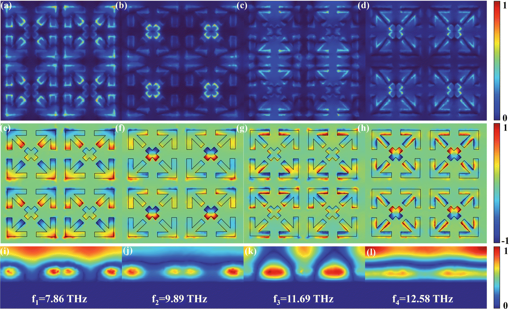
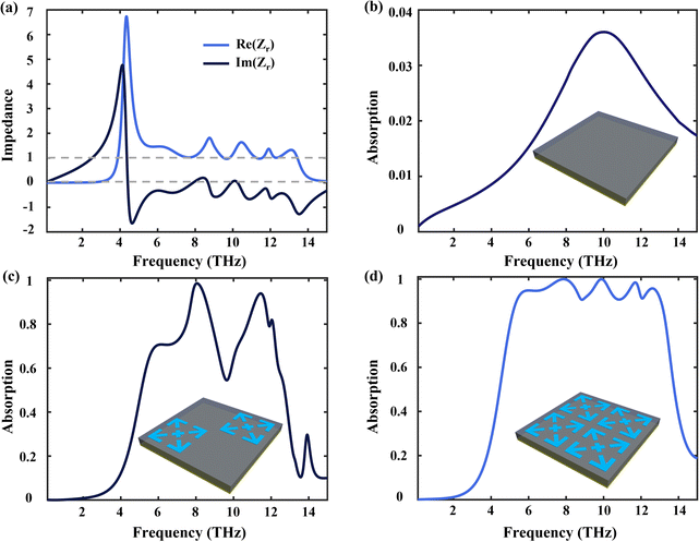
In order to investigate the operating mechanism of the absorber in depth, we plot the electromagnetic field distribution of four absorption peaks (f1, f2, f3, and f4) under TE polarized waves. Fig. 5(a)–(d) show the normalized lateral electric field distribution (|E|) at the dielectric layer/VO2 pattern layer interface (z = 5 μm). It is worth noting that the electric field intensity distribution varies significantly at different resonant frequencies, while conveying the unique coupling information of the absorber. For a single absorption peak, the electric field intensity is mainly distributed around the arrows and crosses of each VO2 resonant structure. Fig. 5(e)–(h) show the normalized real parts (real(Ez)) of the z-component of the electric field distribution at four resonant frequencies. As shown in Fig. 5(e), at the lowest resonance frequency f1, the positive and negative charges are mainly accumulated in the lateral positions of the arrow head and tail of a single pattern, thus forming dipole resonance. Due to the presence of opposite charges on the patterned surface, the presence of electric dipole resonance is closely associated with the excited localized surface plasmon resonance at the dielectric layer/VO2 pattern layer interface. As shown in Fig. 5(f), for the absorption peak f2, the electric field mainly concentrates on the center position of the four overall patterns, thus forming multi-dipole resonance. As shown in Fig. 5(g), for the absorption peak f3, the positive and negative charges are mainly gathered on both sides of the edges of the upper and lower adjacent resonant structures. Because of the interaction between the upper and lower two identical patterns, a multiple dipole resonance is consequently excited. At the absorption peak f4, as shown in Fig. 5(h), the positive and negative charges are roughly concentrated at the inner structure edges of the four overall patterns. In fact, the resonant modes at this frequency are mainly composed of complex pattern interactions, which can be attributed to the multi-dipole resonance between the upper and lower single patterns and between the up and down arrows within a single pattern. Fig. 5(i)–(l) show the normalized electric field distribution (Exz) in the plane y = 0. The electric field intensity is mainly concentrated in the dielectric layer and the VO2 resonant structure. Overall, the physical mechanism of the near-perfect ultra-broadband terahertz absorber stems from the surface plasmon resonance generated by the surface charge of VO2, which is gradually depleted in the dielectric layer between the VO2 structure and the gold film.
 |
| | Fig. 5 The normalized electric field distribution (|E|) along the xy cross-section (z = 5 μm) of the absorber is extracted when VO2 is in the metallic state. Among them, (a) f1 = 7.86 THz, (b) f2 = 9.89 THz, (c) f3 = 11.69 THz, and (d) f4 = 12.58 THz. (e)–(h) Normalized real parts (real(Ez)) of the z-component of the electric field distribution at the four resonant frequencies. (i)–(l) Normalized electric field distributions on the xz cross-section (y = 0) at the four resonant frequencies. | |
The optimized geometric parameters make the absorber have excellent absorption performance. To demonstrate that the designed absorber is somewhat reasonable, we followed the principle of controlling other parameters to be constant and varying a single parameter to study the effect of geometric parameters on the performance of the absorber. Fig. 6(a)–(f) illustrate the differences in the absorption peaks generated by the arrow width w1, the spacing w2 of the adjacent arrows, the interval w3 between the diagonal arrows and the middle cross, the interval d1 between the adjacent VO2 synthetic patterns, and the periods (P and P1), respectively. As shown in Fig. 6(a), as the width of the arrow of the VO2 hybrid patterns increases, the absorption bandwidth of the absorber grows continuously, while the absorption intensity of the absorption peaks remains basically unchanged. The main reason is that different resonance intensities are generated between VO2 patterns with different widths and terahertz waves, thus achieving broadband absorption. As shown in Fig. 6(b), when the spacing w2 between the adjacent arrows changes from 3.3 μm to 4.6 μm, the high frequency absorption and absorption bandwidth have little effect. However, there is a blue shift in the absorption at low and mid frequencies. This is due to the fact that the longer the arrow, i.e., the smaller w2, the more favourable the terahertz wave resonates with the VO2 structure in the low- and mid-frequency regions. As shown in Fig. 6(c), the size of w3 affects the absorption intensity of the absorption peak and produces the opposite results for the absorption bandwidth of low and high frequencies. Fig. 6(d) shows that increasing the distance between each VO2 pattern has little effect on the low-frequency absorption. Moreover, the larger the d1 is, the absorption spectrum is gradually blue-shifted, and the absorption bandwidth is relatively increased. We can see from Fig. 6(e and f) that the larger the period P, the greater the absorption bandwidth, but the optimal value of P1 can only float within a small range of 20 μm.
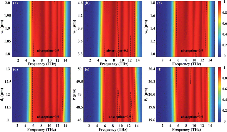 |
| | Fig. 6 When VO2 is in the metallic state, the influences of changing the geometric parameters of the absorber on the absorption spectrum are investigated with other parameters remain unchanged. The geometric parameters are as follows: (a) the arrow width w1, (b) the spacing w2 of the adjacent arrows, (c) the interval w3 between the diagonal arrows and the middle cross, (d) the interval d1 between the adjacent VO2 patterns, and (e) and (f) the unit cell and the period of a single VO2 pattern, respectively. | |
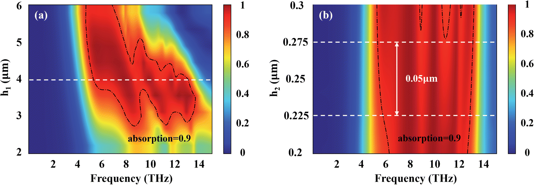
Next, we explore the influences of changing the thickness h1 of the dielectric layer and the height h2 of the VO2 pattern on the designed absorber when VO2 is in the metallic state. In Fig. 7, we mark the contours of 90% absorption with dotted lines. It can be seen from Fig. 7(a) that the absorption rate is gradually strengthened with the increase of h1 from 2 μm to 6 μm. It can be found that when h1 increases to about 4 μm more than 90% of the absorption bandwidth reaches as wide as 7.7 THz from 5.36 THz to 13.06 THz (indicated by the white dashed line), and then the bandwidth gradually decreases. It can be seen from Fig. 7(b) that the absorber achieves ultra-broadband absorption when the height h2 is increased from 0.2 μm to 0.3 μm, and the absorption efficiency is above 90%. Besides, the pattern thickness h2 maintains the best absorption effect within the variation range of 0.05 μm, which exhibits insensitivity with a slight impact on the absorber.
 |
| | Fig. 7 (a) The absorption spectra of changing the thickness of the middle dielectric layer from 2 μm to 6 μm when the conductivity of VO2 is 2 × 10⁵ S m−1. (b) Absorption spectra as the thickness of VO2 varies from 0.2 μm to 0.3 μm when the conductivity of VO2 is 2 × 10⁵ S m−1. | |
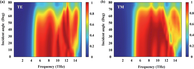
In combination with the diversity of electromagnetic simulations in realistic environments, higher standards have been established for the environmental adaptation of ultra-broadband terahertz absorbers. Fig. 8 shows the multi-angle absorption spectra of the designed absorber in TE and TM polarization modes over the range of incidence angles from 0° to 80°. As shown in Fig. 8(a), for TE polarization, the absorption amplitude remains above 80% as the angle of incidence changes from 0° to 40°, and the absorption bandwidth increases accordingly. The absorption rate remains at a higher level in a certain frequency range with an increasing angle of incidence. The absorbance gradually decreases at high incident angles. As illustrated in Fig. 8(b), for TM polarization, the bandwidth tends to narrow as the angle of incidence increases. However, the absorptivity is always above 80% when the incidence angle increases to 60°, thus achieving wide-angle absorption. Some high-order modes appear when the incidence angle is greater than 18°, and the overall absorption effect is not as good as the TE mode. The main reason is that under TM polarization, the interaction between the VO2 pattern layer and the bottom metal is weakened due to the decrease of the tangential component of the electric field with the increasing angle of incidence. The electromagnetic wave energy is not better bound in the dielectric layer, so there is a part of the energy loss.
 |
| | Fig. 8 The absorption spectra under different incidence angles for (a) TE polarization and (b) TM polarization when the conductivity of VO2 is 2 × 10⁵ S m−1. | |
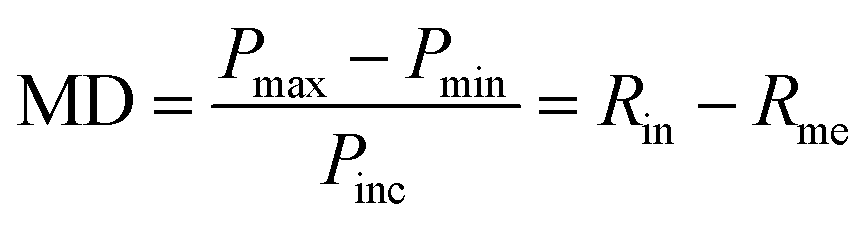
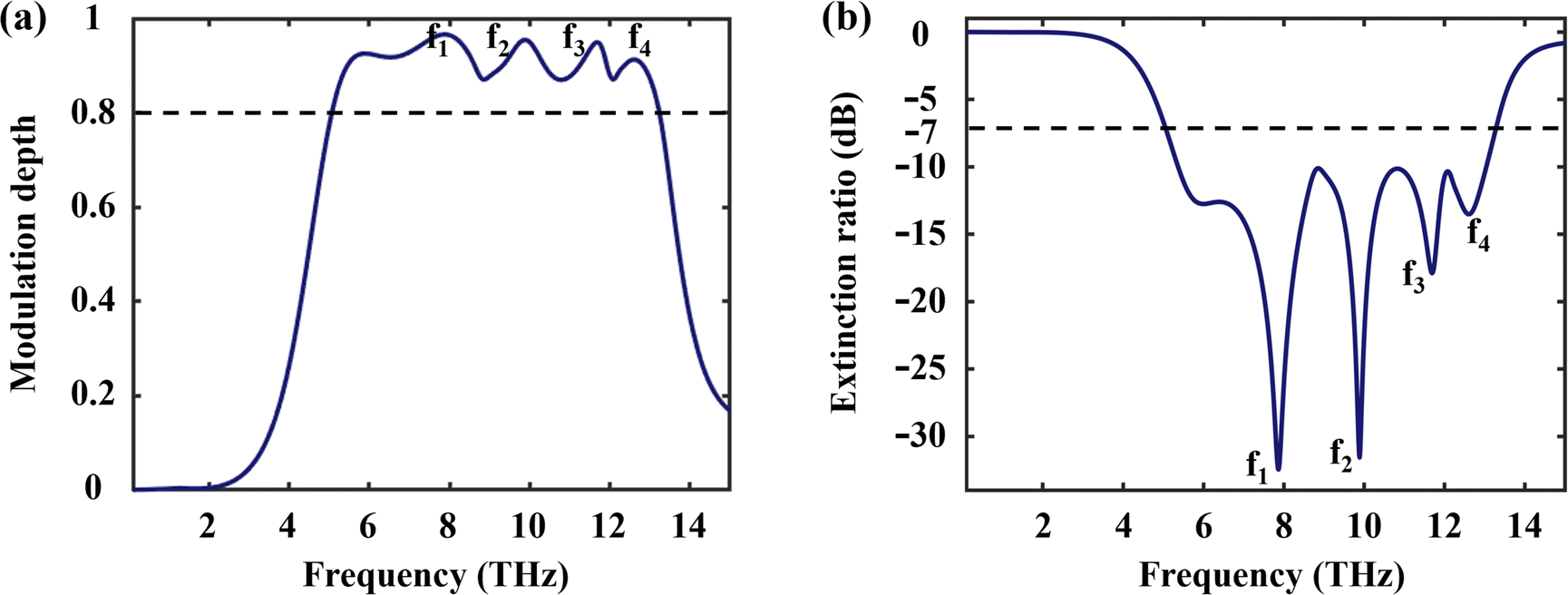
Finally, considering that the designed absorber is to be practically applied in fields such as broadband optical modulators, we need to choose an appropriate figure of merit to measure the performance of the modulator design. The modulation depth (MD) and extinction ratio (ER) are important indicators to characterize optical modulators,67,68 which are generally defined as follows:
| |  | (5) |
| |  | (6) |
where
Pmax, and
Pmin and
Pinc are the maximum reflected power (when VO
2 is in the insulation state), the minimum reflected power (when VO
2 is in the metal state), and the incident power, respectively.
Rin and
Rme are the reflectance of the modulator when VO
2 is in the insulation and metal states, respectively. It can be clearly observed from
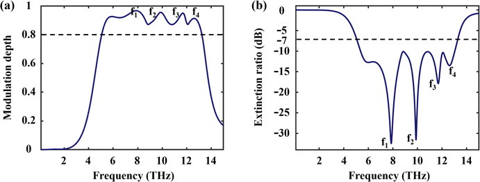
Fig. 9(a) that the MD corresponding to the four absorption peaks
f1,
f2,
f3, and
f4 are 0.97, 0.95, 0.95 and 0.91, respectively. The frequency range corresponding to the MD of the absorber greater than 0.8 is 5.07–13.22 THz. To satisfy the practical needs of people, an ER od less than −7 dB is the design requirement of a typical modulator.
68 As shown in
Fig. 9(b), the corresponding ER of the four absorption peaks
f1,
f2,
f3, and
f4 are −32.38, −31.43, −17.87 and −13.5, respectively. The absorber is below −7 dB corresponding to a frequency range of 5.04–13.29 THz. On the whole, the designed absorber is better to achieve the expected goals and exhibit better modulation performance. Therefore, the flexible design method of this absorber provides a broad application prospect for optical modulators.
 |
| | Fig. 9 (a) MD and (b) ER of the designed absorber as a function of frequency in the operating band, respectively. | |
Conclusion
In conclusion, we proposed and numerically demonstrated an ultra-wideband terahertz perfect absorber based on a hybrid patterned VO2 metamaterial. The absorber consists of a typical three-layer structure, which consists of a metal reflective layer, a dielectric layer and a patterned VO2 structure. The results indicate that the terahertz absorber has more than 90% absorption in the frequency range of 5.2–13.03 THz when VO2 is in the metallic state, and the absorption bandwidth can reach 7.7 THz. The absorber achieves near-perfect amplitude modulation as the conductivity of VO2 changes from 200 S m−1 to 2 × 10⁵ S m−1, and its absorption can be dynamically tuned from 4.31% to 100%. The absorber is characterized by polarization insensitivity and wide-angle absorption due to the symmetrical resonant mode. Compared with recently reported absorbers, the terahertz absorber offers significant improvements in both tunable performance and absorption bandwidth. Moreover, the MD and ER of the absorber both meet the application requirements of optical modulators. In addition, our designed simple structure is easy to process and fabricate. Therefore, this high-performance ultra-broadband terahertz absorber has great promise for applications in modulation, stealth technology, and energy harvesting.
Author contributions
The authors have contributed to this article in the following way: Xiaoju Xue constructed the synthesized VO2 pattern, designed an ultra-broadband terahertz absorber using the numerical simulation software, and confirmed the feasibility of the absorber design through simulation and optimization. Bijun Xu supervised the entire project from conception to realization and gave theoretical guidance and confirmed character layouts. Dandan Chen investigated the special properties of the phase change material VO2 in advance and proposed an effective method to design the absorber. Xiaogang Wang was responsible for analyzing the results of the data presented by the absorber and providing ideas for help. Jun Wu and Ying Hao provided specific details for writing ideas and reviewing the manuscript.
Conflicts of interest
There are no conflicts of interest to declare.
Acknowledgements
This work was supported by the National Natural Science Foundation of China (61975185).
Notes and references
- S. Komiyama, IEEE J. Sel. Top. Quantum Electron., 2010, 17, 54–66 Search PubMed.
- I. F. Akyildiz, J. M. Jornet and C. Han, Phys. Commun., 2014, 12, 16–32 CrossRef.
- Z. D. Taylor, R. S. Singh, D. B. Bennett, P. Tewari, C. P. Kealey, N. Bajwa, M. O. Culjat, A. Stojadinovic, H. Lee and J.-P. Hubschman, IEEE Trans. Terahertz Sci. Technol., 2011, 1, 201–219 Search PubMed.
- Y. Liu, M. Bo, X. Yang, P. Zhang, C. Q. Sun and Y. Huang, Phys. Chem. Chem. Phys., 2017, 19, 5304–5309 RSC.
- T. Driscoll, H.-T. Kim, B.-G. Chae, B.-J. Kim, Y.-W. Lee, N. M. Jokerst, S. Palit, D. R. Smith, M. Di Ventra and D. N. Basov, Science, 2009, 325, 1518–1521 CrossRef.
- J. B. Pendry, A. Holden, W. Stewart and I. Youngs, Phys. Rev. Lett., 1996, 76, 4773 CrossRef PubMed.
- Y. Liu and X. Zhang, Chem. Soc. Rev., 2011, 40, 2494–2507 RSC.
- B. Xu, C. Wu, Z. Wei, Y. Fan and H. Li, Opt. Mater. Express, 2016, 6, 3940–3945 CrossRef.
- Z. Sun, B. Xu, F. Jin, G. Zhou and L. Lin, IEEE J. Sel. Top. Quantum Electron., 2021, 28, 1–9 Search PubMed.
- K. Iwaszczuk, A. C. Strikwerda, K. Fan, X. Zhang, R. D. Averitt and P. U. Jepsen, Opt. Express, 2012, 20, 635–643 CrossRef.
- W. Xu, L. Xie and Y. Ying, Nanoscale, 2017, 9, 13864–13878 RSC.
- P. Mookiah and K. R. Dandekar, IEEE Trans. Antennas Propag., 2009, 57, 3283–3292 Search PubMed.
- L. Wu, X. Zhang, Y. Fu, K. Kang, X. Ding, J. Yao, Z. Wang, J. Han and W. Zhang, Adv. Photonics Res., 2022, 2200033 CrossRef.
- J. Hunt, T. Driscoll, A. Mrozack, G. Lipworth, M. Reynolds, D. Brady and D. R. Smith, Science, 2013, 339, 310–313 CrossRef CAS.
- H. Tao, N. I. Landy, C. M. Bingham, X. Zhang, R. D. Averitt and W. J. Padilla, Opt. Express, 2008, 16, 7181–7188 CrossRef.
- Z. Wu, B. Xu, M. Yan, B. Wu, Z. Sun, P. Cheng, X. Tong and S. Ruan, Plasmonics, 2020, 15, 1863–1867 CrossRef CAS.
- M.-Y. Yan, B.-J. Xu, Z.-C. Sun, Z.-D. Wu and B.-R. Wu, Chin. Phys. Lett., 2020, 37, 067801 CrossRef.
- M. Gil, J. Bonache and F. Martin, Metamaterials, 2008, 2, 186–197 CrossRef.
- H.-T. Chen, W. J. Padilla, M. J. Cich, A. K. Azad, R. D. Averitt and A. J. Taylor, Nat. Photonics, 2009, 3, 148–151 CrossRef CAS.
- X.-J. Xue, B.-J. Xu, B.-R. Wu, X.-G. Wang, X.-N. Yu, L. Lin and H.-Q. Li, Chin. Phys. B, 2022 DOI:10.1088/1674-1056/ac7cd0.
- M. Diem, T. Koschny and C. M. Soukoulis, Phys. Rev. B, 2009, 79, 033101 CrossRef.
- P. Nie, D. Zhu, Z. Cui, F. Qu, L. Lin and Y. Wang, Sens. Actuators, B, 2020, 307, 127642 CrossRef.
- L. Wu, T. Du, N. Xu, C. Ding, H. Li, Q. Sheng, M. Liu, J. Yao, Z. Wang and X. Lou, Small, 2016, 12, 2609 CrossRef.
- R. Jadeja, S. Charola, S. K. Patel, J. Parmar, M. Ladumor, T. K. Nguyen and V. Dhasarathan, J. Mater. Sci., 2020, 55, 3462–3469 CrossRef.
- N. I. Landy, S. Sajuyigbe, J. J. Mock, D. R. Smith and W. J. Padilla, Phys. Rev. Lett., 2008, 100, 207402 CrossRef PubMed.
- C.-W. Cheng, M. N. Abbas, C.-W. Chiu, K.-T. Lai, M.-H. Shih and Y.-C. Chang, Opt. Express, 2012, 20, 10376–10381 CrossRef PubMed.
- W. Li, T. Wu, W. Wang, J. Guan and P. Zhai, Appl. Phys. Lett., 2014, 104, 022903 CrossRef.
- S. Liu, H. Chen and T. J. Cui, Appl. Phys. Lett., 2015, 106, 151601 CrossRef.
- Z. Su, J. Yin and X. Zhao, Opt. Express, 2015, 23, 1679–1690 CrossRef PubMed.
- L. Wang, S. Ge, W. Hu, M. Nakajima and Y. Lu, Opt. Express, 2017, 25, 23873–23879 CrossRef PubMed.
- Z. Wu, B. Xu, M. Yan, B. Wu, P. Cheng and Z. Sun, Opt. Mater. Express, 2021, 11, 73–79 CrossRef.
- B. Tang and Y. Ren, Phys. Chem. Chem. Phys., 2022, 24, 8408–8414 RSC.
- J. Yang, P. Wang, T. Shi, S. Gao, H. Lu, Z. Yin, W. Lai and G. Deng, Opt. Express, 2019, 27, 27039–27045 CrossRef CAS PubMed.
- G. Deng, H. Hu, H. Mo, Z. Yin, H. Lu, M. Hu, J. Li and J. Yang, Opt. Express, 2022, 30, 22550–22561 CrossRef PubMed.
- Z. Li, Y. Yi, D. Xu, H. Yang, Z. Yi, X. Chen, Y. Yi, J. Zhang and P. Wu, Chin. Phys. B, 2021, 30, 098102 CrossRef CAS.
- Z. Li, Z. Yi, T. Liu, L. Liu, X. Chen, F. Zheng, J. Zhang, H. Li, P. Wu and P. Yan, Phys. Chem. Chem. Phys., 2021, 23, 17374–17381 RSC.
- X. Wu, Y. Zheng, Y. Luo, J. Zhang, Z. Yi, X. Wu, S. Cheng, W. Yang, Y. Yu and P. Wu, Phys. Chem. Chem. Phys., 2021, 23, 26864–26873 RSC.
- Y. Zhao, Q. Huang, H. Cai, X. Lin and Y. Lu, Opt. Commun., 2018, 426, 443–449 CrossRef CAS.
- H. Liu, Z.-H. Wang, L. Li, Y.-X. Fan and Z.-Y. Tao, Sci. Rep., 2019, 9, 1–10 CrossRef.
- Z. Zheng, Y. Luo, H. Yang, Z. Yi, J. Zhang, Q. Song, W. Yang, C. Liu, X. Wu and P. Wu, Phys. Chem. Chem. Phys., 2022, 24, 8846–8853 RSC.
- Z. Zheng, Y. Zheng, Y. Luo, Z. Yi, J. Zhang, Z. Liu, W. Yang, Y. Yu, X. Wu and P. Wu, Phys. Chem. Chem. Phys., 2022, 24, 2527–2533 RSC.
- Z. Shao, X. Cao, H. Luo and P. Jin, NPG Asia Mater., 2018, 10, 581–605 CrossRef.
- F. Z. Shu, J. N. Wang, R. W. Peng, B. Xiong, R. H. Fan, Y. J. Gao, Y. Liu, D. X. Qi and M. Wang, Laser Photonics Rev., 2021, 15, 2100155 CrossRef CAS.
- W. J. Kort-Kamp, S. Kramadhati, A. K. Azad, M. T. Reiten and D. A. Dalvit, ACS Photonics, 2018, 5, 4554–4560 CrossRef CAS.
- X. Xue, B. Xu, B. Wu, X. Wang, X. Yu, L. Lin and H. Li, Opt. Express, 2022, 30, 20389–20400 CrossRef CAS.
- S. Choi, J. Kyoung, H. Kim, H. R. Park, D. Park, B.-J. Kim, Y. Ahn, F. Rotermund, H.-T. Kim and K. Ahn, Appl. Phys. Lett., 2011, 98, 071105 CrossRef.
- Y. Sun, Y. Shi, X. Liu, J. Song, M. Li, X. Wang and F. Yang, Nanoscale Adv., 2021, 3, 4072–4078 RSC.
- N. A. Butakov, I. Valmianski, T. Lewi, C. Urban, Z. Ren, A. A. Mikhailovsky, S. D. Wilson, I. K. Schuller and J. A. Schuller, ACS Photonics, 2018, 5, 371–377 CrossRef CAS.
- Q.-Y. Wen, H.-W. Zhang, Q.-H. Yang, Y.-S. Xie, K. Chen and Y.-L. Liu, Appl. Phys. Lett., 2010, 97, 021111 CrossRef.
- Y. Zhang, Y. Feng and J. Zhao, Carbon, 2020, 163, 244–252 CrossRef CAS.
- T. Lv, Y. Li, H. Ma, Z. Zhu, Z. Li, C. Guan, J. Shi, H. Zhang and T. Cui, Sci. Rep., 2016, 6, 1–9 CrossRef PubMed.
- Z. Song, K. Wang, J. Li and Q. H. Liu, Opt. Express, 2018, 26, 7148–7154 CrossRef CAS PubMed.
- R. Zhou, T. Jiang, Z. Peng, Z. Li, M. Zhang, S. Wang, L. Li, H. Liang, S. Ruan and H. Su, Opt. Mater., 2021, 114, 110915 CrossRef.
- W. Liu, J. Xu and Z. Song, Opt. Express, 2021, 29, 23331–23340 CrossRef PubMed.
- R.-n Dao, X.-r Kong, H.-f Zhang and X.-r Su, Optik, 2019, 180, 619–625 CrossRef.
- J. Bai, S. Zhang, F. Fan, S. Wang, X. Sun, Y. Miao and S. Chang, Opt. Commun., 2019, 452, 292–295 CrossRef.
- X.-F. Jiao, Z.-H. Zhang, T. Li, Y. Xu and G.-F. Song, Appl. Sci., 2020, 10, 7259 CrossRef.
- J. Huang, J. Li, Y. Yang, J. Li, J. Li, Y. Zhang and J. Yao, Opt. Express, 2020, 28, 17832–17840 CrossRef PubMed.
- H. Zhang, F. Ling and B. Zhang, Opt. Mater., 2021, 112, 110803 CrossRef CAS.
- X. Dong, X. Luo, Y. Zhou, Y. Lu, F. Hu, X. Xu and G. Li, Opt. Express, 2020, 28, 30675–30685 CrossRef CAS PubMed.
- S. Wang, L. Kang and D. H. Werner, Sci. Rep., 2017, 7, 1–8 CrossRef PubMed.
- F. Fan, Y. Hou, Z.-W. Jiang, X.-H. Wang and S.-J. Chang, Appl. Opt., 2012, 51, 4589–4596 CrossRef PubMed.
- C. Wu, F. Feng and Y. Xie, Chem. Soc. Rev., 2013, 42, 5157–5183 RSC.
- H.-T. Chen, Opt. Express, 2012, 20, 7165–7172 CrossRef PubMed.
- D. Smith, D. Vier, T. Koschny and C. Soukoulis, Phys. Rev. E, 2005, 71, 036617 CrossRef PubMed.
- C. Cen, Z. Chen, D. Xu, L. Jiang, X. Chen, Z. Yi, P. Wu, G. Li and Y. Yi, Nanomaterials, 2020, 10, 95 CrossRef PubMed.
- B. Zhang, Y. Zhao, Q. Hao, B. Kiraly, I.-C. Khoo, S. Chen and T. J. Huang, Opt. Express, 2011, 19, 15221–15228 CrossRef CAS PubMed.
- S. G.-C. Carrillo, G. R. Nash, H. Hayat, M. J. Cryan, M. Klemm, H. Bhaskaran and C. D. Wright, Opt. Express, 2016, 24, 13563–13573 CrossRef PubMed.
|
| This journal is © the Owner Societies 2023 |
Click here to see how this site uses Cookies. View our privacy policy here. 
 b,
Hao
Ying
c and
Bijun
Xu
b,
Hao
Ying
c and
Bijun
Xu


 (λ0 is the resonance wavelength of free space, and n and ε are the refractive index and dielectric constant of SiO2, respectively). Here, the resonance wavelength of free space is λ0 = c/fc, and the corresponding dielectric layer thickness is d ≈ 4.18 μm. In the numerical simulation, the optimized value of the actual thickness of the intermediate media compartment is h1 = 4 μm, which has a small difference with the theoretical calculation result, and the designed absorber is more in line with the interference elimination conditions.
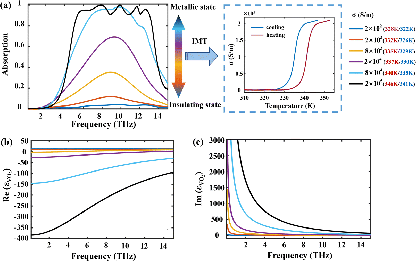

 is the effective impedance of the absorber and Z0 is the effective impedance of the free space. As shown in Fig. 4(a), we plotted the relative impedance variation curves when the conductivity of VO2 is 2 × 10⁵ S m−1 in the operating frequency range. It can be seen from the figure that in the frequency range from 0.1 THz to 15 THz, the real and imaginary parts of the relative impedance of the absorber tend to be 1 and 0, respectively (i.e., Zr = 1). Thus, the absorption rate A(ω) = 1, which makes the results closer to the ideal cases. This also indicates that the effective impedance of the absorber and the impedance of the free space are matched to reach the maximum absorption bandwidth and achieve perfect absorption. In essence, the incident electromagnetic wave is continuously reflected at the upper and lower interfaces of the intermediate dielectric layer, which leads to the complete consumption of the electromagnetic energy and the confinement of the light beam in the dielectric. Additionally, we separately demonstrate the effect of hybrid VO2 patterns on the overall absorption performance of absorbers (e.g., unpatterned absorbers, two-patterned absorbers, and four-patterned absorbers). Fig. 4(b) shows an unpatterned absorber consisting of only a metal ground layer and a dielectric layer. The simulation results show that the absorber produces a weak single peak with less than 3.6% absorptance. The addition of the VO2 pattern slightly improves the absorption performance compared to the absorber when VO2 is in the insulating state (σ = 200 S m−1). As shown in Fig. 4(c), we further added two identical VO2 patterns arranged in a diagonally symmetric manner. The results show that the absorber produces two perfect absorption peaks at 8.06 THz and 11.44 THz, with absorption rates of 98.5% and 94%, respectively. Compared with the unpatterned absorber, the absorption performance of the absorber is significantly enhanced. This is attributed to the continuous consumption of energy after the terahertz wave resonates in the metal–dielectric–metal structure, which achieves an increase in the absorption rate. Fig. 4(d) shows that the absorber produces four perfect absorption peaks when four resonant structures of the same size are combined on a single unit. In addition, both the absorption rate and the absorption bandwidth have reached the highest values compared to the previous ones.