
Lead-free double perovskites: how divalent cations tune the electronic structure for photovoltaic applications†
Ismail A. M.
Ibrahim
 ab and
Chan-Yeup
Chung
a
ab and
Chan-Yeup
Chung
a
aDivision of Carbon Neutrality & Materials Digitalization, Korea Institute of Ceramic Engineering & Technology, Jinju 52851, South Korea. E-mail: ibrahim@kicet.re.kr; chanyeup@kicet.re.kr
bDepartment of Chemistry, Faculty of Science, Helwan University, 11795 Cairo, Egypt. E-mail: ismail.ibrahim@science.helwan.edu.eg
First published on 2nd August 2022
Abstract
Recently, the efficiency of perovskite-based solar cells has reached 25.7%. Due to lead toxicity, lead-free double perovskites have received great attention as potential candidates for photovoltaic applications. Keeping in mind the significant challenges (indirect and wide bandgaps) related to most of the present double perovskites, we used ab initio calculations and incorporated divalent and tetravalent dopant cations at the mixed B-site of Cs2AgSbCl6 to tune the electronic structure for optoelectronic applications. The doped perovskites are structurally and thermodynamically stable. The tunability of the electronic structure is shown for Sn2+- and Ge2+-doped configurations due to the strong hybridization between the dopant orbitals (s2p0) and the host orbitals at the band edges. The predicted bandgaps of the doped perovskites are of a direct character and in the ideal range (1.70–1.90 eV) for the top cell in tandem solar cells. The inclusion of Zn2+, Cd2+, Sn4+, and Ge4+ with the electronic configurations of d10s0 and s0p0 resulted in a negligible modification of the electronic structure, and hence did not show an indirect–direct bandgap transition. Therefore, the contribution from the dopant orbitals at the band edges dominates the electronic structure tunability of the doped perovskites. Furthermore, an enhanced absorption efficiency is observed for the Sn2+- and Ge2+-doped perovskites. This work provides a computational guide for exploring low-cost and non-toxic dopants for the electronic structure-engineering of double perovskites as photo-absorbers in future solar cell applications.
1. Introduction
Lead halide perovskites have been extensively utilized in energy applications such as photovoltaic cells1,2 and light-emitting diodes3,4 due to their promising optoelectronic and physical properties and their low-cost. Generally, perovskite-based solar cells have achieved clear performance improvements in recent years, and the power conversion efficiency (PCE) has been increased to 25.7%.5 Furthermore, perovskites integrated into silicon tandem cells have achieved a cell efficiency of 29.8%, which exceeds that of crystalline silicon-based solar cells.5 Therefore, perovskites with ABX3 structures (A = methylammonium (MA), formamidinium (FA), Cs or Rb; B = Pb, Sn or Ge; and X = I, Cl or Br) are considered as the most promising candidates for third-generation photovoltaic cells due to their ability as efficient light absorbers.6 Among lead halide perovskites, MAPbI3-based solar cells have shown extremely high PCE values.6 Despite the advantages of lead halide perovskites, there are many concerns due to the presence of toxic lead, which affects the application of these perovskites.7 The straightforward chemical modification of lead iodide perovskites is through substituting lead with Sn or Ge. However, due to the tendency of Sn toward oxidation from the +2 to the +4 oxidation state upon exposure to air, tin halide perovskite-based photovoltaic cells have achieved a PCE of only 6%.8 Recently, to enhance the stability of mixed lead halide perovskite-based photovoltaic cells and improve their PCE, composition ratios of mixed lead halide perovskites have been systematically investigated.9 The mixed lead halide perovskite FA0.75Cs0.25Sn0.5Pb0.5I3 was reported to have outstanding thermal and atmospheric stability.10Recently, lead-free double perovskites A2B′B′′X6 (B′ = Ag, K; and B′′ = Bi, In, Sb), with a combination of monovalent and trivalent cations, have been received intensive attention as potential photovoltaic absorbers and as candidates in optoelectronic applications.11–13 Cs2AgBiBr6 is one of the most widely reported double perovskites as a promising candidate for photovoltaic applications.12,14 However, its bandgap value is 1.9–2.3 eV, which still large for use in tandem solar cells.15 The ideal bandgap range for top cells in tandem solar cells is 1.7–1.9 eV.16 In addition, Cs2AgBiBr6 is an indirect bandgap semiconductor and the light absorption due to the direct-gap transition is very weak.6,17,18 The indirect bandgap provides weak oscillator strengths for optical absorption and radiative recombination, and therefore makes a negligible contribution to the photo-generated carriers.6 The use of thicker films could increase the absorption efficiency; however, this could also be problematic in the case of a low charge-carrier mobility and a limited charge-diffusion length as in Cs2AgBiBr6.12
Reported chloride double perovskites such as Cs2AgSbCl6 and Cs2AgBiCl6 typically have wide indirect bandgaps of 2.54 eV19 and 2.77 eV,20 respectively, which are too large for photovoltaic applications.21,22 Therefore, an increased visible-light absorption efficiency via reduction of the bandgap is required for future applications of these perovskites in optoelectronic technologies.23,24 Recently, the Cs2AgSbCl6 double perovskite has been reported to have a high decomposition temperature and high stability upon prolonged exposure to air and moisture; therefore, it was proposed as a potential candidate in photovoltaic applications.11 Therefore, most of the current double perovskite materials still suffer from indirect or wide bandgaps, which need to be addressed to further advance the performance of solar cells. The challenge is, therefore, how to rationally design or engineer the electronic structure of the double perovskites in order to obtain a small bandgap and an indirect-to-direct bandgap transition. There are many strategies for optimization of the perovskite electronic structure, such as impurity and pressure strategies.25–27
In double perovskites with the A2B′B′′X6 structure, all four different lattice sites are available for atomic substitution.28 A very low doping concentration results in localized dopant states in the host lattice where the potential extends around the dopant atom; therefore, this leads to a shift in the Femi level and changes the bandgap slightly.6 To effectively tune the bandgap, the perovskite lattice may need a sufficient doping concentration in order to provide localized impurity states that interact with each other and the states of the host lattice.6 The doping strategy has been reported in engineering the bandgap of semiconductors and perovskites.29–32 In the Cs2AgBiBr6 double perovskite, bandgap engineering was reported experimentally and theoretically using Sb3+ and In3+ substitution at the trivalent Bi lattice site.25 The doped perovskite lattice accommodated up to 75% of In3+ with an increased bandgap and up to 37.5% of Sb3+ with a reduced bandgap.25 Furthermore, the Cs2(Ag1−aBi1−b)TlxBr6 double perovskite with Tl doping at Ag+ and Bi3+ sites was reported experimentally and exhibits a comparable bandgap and carrier lifetime to that of (MA)PbI3, although there are concerns due to the use of the highly toxic Tl element.14 Moreover, In3+-incorporated Cs2AgSbCl6 double perovskites were synthesized experimentally with high In concentrations of 50, 60, 80, and 100%, which showed indirect–direct bandgap transitions.19 Given all of these previous observations, further efforts that focus on electronic-structure engineering using a doping strategy could enable double perovskites to play an important role in future optoelectronic applications.
Double perovskites (A2B′B′′X6) can support oxidation states from 1+ to 4+ for B metal sites, and this compositional versatility should result in diverse and tuned electronic structures. In this work, we present a computational methodology for the electronic-structure engineering of the lead-free Cs2AgSbCl6 double perovskite through a doping strategy using divalent cations (M = Sn2+, Ge2+, Zn2+, and Cd2+) for photovoltaic applications. The dopant cations (Sn, Ge, Zn, and Cd) were selected to have comparable electronic configurations to the Ag and Sb cations. Therefore, we can adjust the contribution of the Ag and Sb orbitals at the top of the valence band and the bottom of the conduction band in order to control the bandgap character. Two dopant atoms are considered to replace one Ag atom and one Sb atom with a doping ratio of 25%. Furthermore, the presence of M4+ ions is also considered in order to elucidate the role of the dopant atom oxidation state on the electronic-structure engineering. The structure properties, decomposition energy, and formation energy are calculated to reveal the structural changes and stability of the doped perovskites. Through calculation of the electronic properties, we present a systematic description of the induced dopant levels and the interaction between the dopant and the host orbitals, in order to find the underlying factor for the bandgap transition of the cation-doped Cs2AgSbCl6 perovskites. Then, the electronic structure could be tuned by selecting a suitable dopant using first principles calculations. Therefore, in silico electronic-structure engineering based on first principles calculations would help to decrease the number of rather expensive experiments and speed up the search for suitable dopants. Finally, the optical absorption spectra are calculated via the frequency-dependent dielectric function to account for the optical performance of pristine and M-doped Cs2AgSbCl6 double perovskites for solar cells.
2. Computational methodology
Periodic spin-polarized density functional theory (DFT) calculations were carried out using the Vienna ab initio simulation package (VASP).33,34 The core–valence interaction is described using Blöchl's projector augmented wave (PAW) approach.35 Exchange–correlation energies were calculated using the Perdew–Burke–Ernzerhof (PBE) functional36 based on the generalized gradient approximation (GGA) for geometrical optimization with a stopping criterion of 10−5 eV for the electronic minimization loop, and the width of Gaussian smearing is 0.05 eV. Plane-wave basis sets were used to expand the valence electrons for Cs: 5s25p66s1, Ag: 4d105s1, Sb: 5s25p3, Sn: 5s25p2, Ge: 4s24p2, Zn: 3d104s2, Cd: 4d105s2, and Cl: 3s23p5. An energy cutoff of 400 eV was used for the plane-wave expansion and a 4 × 4 × 4 Γ-centered Monkhorst–Pack mesh37 was used for sampling the conventional cell in reciprocal space. The optimized volumes were calculated by fitting calculated total energies and volumes to the third-order Birch–Murnaghan equation of states (Fig. S1, ESI†).38 GGA functionals are unable to produce an accurate electronic structure and bandgap for strongly correlated materials; however, the Heyd, Scuseria, and Ernzerhof (HSE) hybrid functional39,40 with the introduction of Hartree–Fock (HF) exchange in the DFT calculations can produce bandgap values that compare well to the experimental results.41 Hence, we applied the HSE hybrid functional to account for the accurate electronic structure and bandgap of the optimized structures. The exact exchange coefficient is 32% and a screening parameter of 0.207 Å−1 was used. The spin–orbit coupling (SOC) effect was considered in these calculations.We investigated the optical properties of pristine and M-doped Cs2AgSbCl6 perovskites by calculating the complex dielectric constant ε at a given frequency using the HSE hybrid functional and the SOC effect. The frequency-dependent dielectric function ε(ω) is given by ε (ω) = ε1(ω) + iε2 (ω), where ε1 and ε2 represent the real and imaginary parts of the dielectric function, respectively, and ω is the photon frequency. The imaginary part ε2(ω) is determined via summation over empty states using the following equation:42
 | (1) |
 | (2) |
 | (3) |
3. Results and discussion
3.1. Doping structure and stability
To thoroughly explore the electronic-structure engineering of cation-doped Cs2AgSbCl6 double perovskites for photovoltaic applications, our calculations considered different doping configurations. The Cs2AgSbCl6 double perovskite is a cubic crystal system with the Fm![[3 with combining macron]](https://www.rsc.org/images/entities/char_0033_0304.gif) m space group. The crystal structure consists of a three-dimensional network of corner-sharing alternating octahedra of [AgCl6] and [SbCl6] with the Cs cations located in the cavities between these octahedra.19 The conventional cell of Cs2AgSbCl6 consists of 8 Cs, 4 Ag, 4 Sb, and 24 Cl atoms, as shown in Fig. S1 (ESI†). To account for the dopant oxidation states we considered different doping configurations. Firstly, two mono-dopant atoms (Sn, Ge, Zn, or Cd) replace one Ag and one Sb atom to give the Cs2Ag1−xSb1−xM2xCl6 doped configuration with M in the divalent oxidation state and a doping ratio of 25% (configuration 1), see Fig. 1. Secondly, the Cs2Ag1−2xMxSbCl6 doped configuration (M = Sn and Ge) was constructed via one dopant atom replacing one Ag atom with the formation of one Ag vacancy (VAg) and the dopant oxidation state is 2+ (configuration 2). The last doping configuration (configuration 3) is constructed to have an M4+ oxidation state through one dopant atom substituting one Sb atom with the formation of one Ag vacancy, resulting in the Cs2Ag1−xSb1−xMxCl6 configuration (M = Sn and Ge). The schematic representation of the three doping configurations is shown in Fig. 1. Furthermore, we considered two different doping motifs by substituting either neighboring or distant Ag and Sb atoms in configuration 1, and by substituting either a neighboring or distant Sb atom from the Ag vacancy in configuration 3 (Fig. 1).
m space group. The crystal structure consists of a three-dimensional network of corner-sharing alternating octahedra of [AgCl6] and [SbCl6] with the Cs cations located in the cavities between these octahedra.19 The conventional cell of Cs2AgSbCl6 consists of 8 Cs, 4 Ag, 4 Sb, and 24 Cl atoms, as shown in Fig. S1 (ESI†). To account for the dopant oxidation states we considered different doping configurations. Firstly, two mono-dopant atoms (Sn, Ge, Zn, or Cd) replace one Ag and one Sb atom to give the Cs2Ag1−xSb1−xM2xCl6 doped configuration with M in the divalent oxidation state and a doping ratio of 25% (configuration 1), see Fig. 1. Secondly, the Cs2Ag1−2xMxSbCl6 doped configuration (M = Sn and Ge) was constructed via one dopant atom replacing one Ag atom with the formation of one Ag vacancy (VAg) and the dopant oxidation state is 2+ (configuration 2). The last doping configuration (configuration 3) is constructed to have an M4+ oxidation state through one dopant atom substituting one Sb atom with the formation of one Ag vacancy, resulting in the Cs2Ag1−xSb1−xMxCl6 configuration (M = Sn and Ge). The schematic representation of the three doping configurations is shown in Fig. 1. Furthermore, we considered two different doping motifs by substituting either neighboring or distant Ag and Sb atoms in configuration 1, and by substituting either a neighboring or distant Sb atom from the Ag vacancy in configuration 3 (Fig. 1).
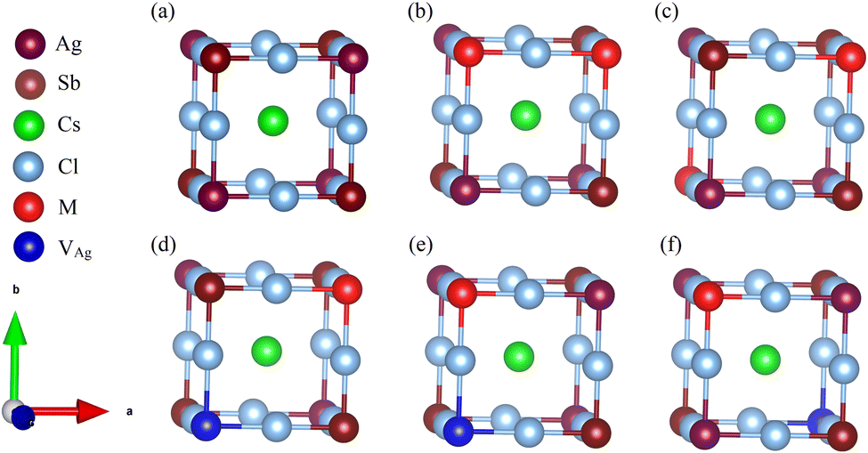 | ||
| Fig. 1 Schematic models of the cubic unit of (a) the pristine Cs2AgSbCl6 conventional cell, (b and c) configuration 1 with neighboring and distant M dopant atoms, respectively, (d) configuration 2, and (e and f) configuration 3 with a neighboring and distant M dopant atom and VAg, respectively. | ||
To explore the relative stability of the different doping configurations, we calculated the dopant formation energy (Eform) using the following equation:45
| Eform = EDoped − EPristine − xμM + yμAg + zμSb | (4) |
The relative stability of the neighboring and separated doping motifs in configuration 1 reveals that when M2+ ions are doped, they prefer to substitute the neighboring Ag+ and Sb3+ ions. Furthermore, in configuration 3, the M4+ cation prefers to substitute the neighboring Sb3+ ion from the Ag+ vacancy. In configuration 3, the doped M4+ can occupy the Ag site; therefore, we also checked the formation of M4+ cations through the substitution of one Ag atom and the formation of one Sb vacancy. However, the M4+–VAg configuration is more stable than the M4+–VSb configuration. Moreover, in our calculations, we did not consider a doping configuration at the interstitial sites, because this has not been reported in doped double perovskites.14,25 The most stable doping configurations were used in our calculations, and the calculated formation energies of these configurations are shown in Fig. 2a. The doped structure with a lower formation energy is the more likely substitution to be formed. As shown in Fig. 2a, among divalent cations, Cd2+–Cd2+ structure has the lowest formation energy and Ge2+–Ge2+ configuration shows the highest formation energy. In addition, the doped structures with tetravalent cations show higher formation energies than the relevant divalent cations. Therefore, the dopant cations prefer to be in a divalent oxidation state when they are incorporated into the Cs2AgSbCl6 host lattice. This conclusion could be preserved with the change of the chemical potential of the host atoms based on the growth conditions.
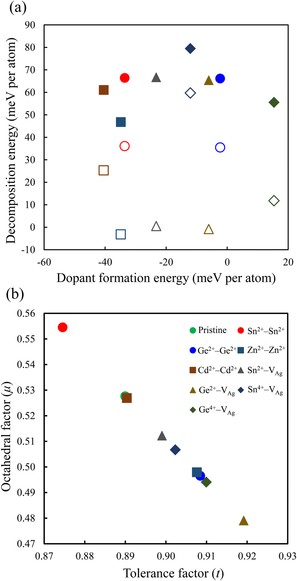 | ||
| Fig. 2 (a) Dopant formation energy vs. decomposition energy, and (b) tolerance factor vs. octahedral factor for the perovskite structures. The filled and empty symbols in (a) represent the decomposition energy using the path in eqn (7) and (8), respectively. | ||
The optimized lattice constants of the pristine and all the doped perovskites are listed in Table 1. The calculated lattice parameter of pristine Cs2AgSbCl6 (a = 10.85 Å) is comparable to the experimental lattice parameter (a = 10.70 Å) and other theoretical calculations (a = 10.83 Å).11,45,46 In configuration 1, we observed a good correlation of the elongation of the lattice constant with the reported value of the ionic radius of Sn2+.47 Moreover, the contraction of the cell volume is shown for Ge2+, Zn2+, and Cd2+, in good agreement with their ionic radii.48 For configurations 2 and 3, the lattice parameters of the relaxed structures are decreased except for the Sn2+–VAg system. In pristine Cs2AgSbCl6, the Ag and Sb atoms are surrounded by six Cl atoms, which leads to the octahedral symmetry as shown in Fig. S2 (ESI†). The calculated Ag–Cl and Sb–Cl bond distances are 2.78 and 2.64 Å, respectively, in agreement with the large ionic radius of the Ag cation compared with the ionic radius of the Sb cation. Upon introduction of the dopant to the pristine perovskite, octahedral distortions that are indicated solely by changes in the bond lengths could be observed due to the ionic size mismatch between the doping cations and the substituted Ag and Sb cations (Fig. S2, ESI†). In addition, the Zn2+–Zn2+ doped system shows the most distorted octahedra with ZnAg–Cl (ZnSb–Cl) bond distances of 2.73 Å (3.15 Å) and 2.23 Å (2.38 Å). Octahedral distortion is reported for the Cs2AgSbCl6 perovskite doped with Cu atoms.45 To further confirm the oxidation state of the dopant cations, we performed Bader charge analysis (Table S1, ESI†).49 The charge associated with the M cations is delocalized from the M center, and hence the Bader charge on the M dopant can only provide a relative and not an absolute value of the M charge state as II or IV.50
| System | Lattice constant a (Å) | Bandgap (eV) | Bandgap character |
|---|---|---|---|
| Pristine | 10.85 | 2.53 | Indirect |
| Sn2+–Sn2+ | 10.97 | 1.78 | Direct |
| Ge2+–Ge2+ | 10.81 | 1.80 | Direct |
| Zn2+–Zn2+ | 10.75 | 2.53 | Indirect |
| Cd2+–Cd2+ | 10.82 | 2.30 | Indirect |
| Sn2+–VAg | 10.94 | 1.88 | Direct |
| Ge2+–VAg | 10.84 | 1.79 | Direct |
| Sn4+–VAg | 10.81 | 2.11 | Indirect |
| Ge4+–VAg | 10.76 | 1.92 | Indirect |
The phase stability of double perovskites can be checked using two empirical parameters. The first is the tolerance factor (t) which is calculated according to the following equation:16,51
 | (5) |
 | (6) |
To study the chemical stability and thermodynamic stability of the doped systems during reaction with external agents such as heat and moisture,16 we calculated the decomposition energy according to the following decomposition paths:8,54
| ΔH = αECsCl + βEAgCl + γESbCl3 + δ EMCli − EDoped | (7) |
| ΔH = αECsCl + βEAgCl + γECs2Sb3Cl9 + δEMCli − EDoped | (8) |
3.2. Electronic-structure engineering
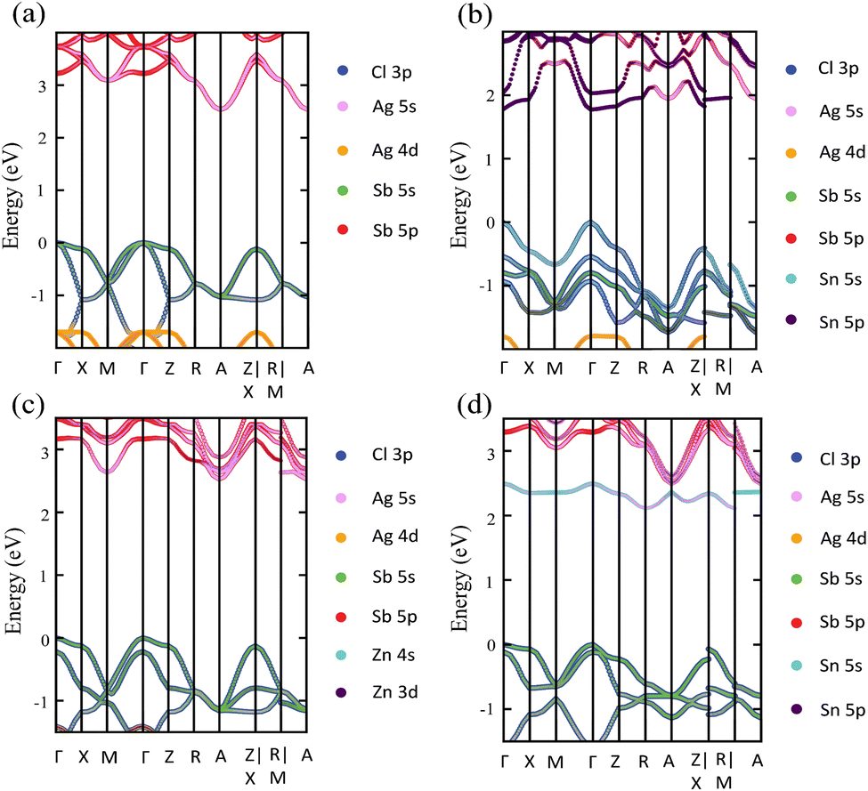
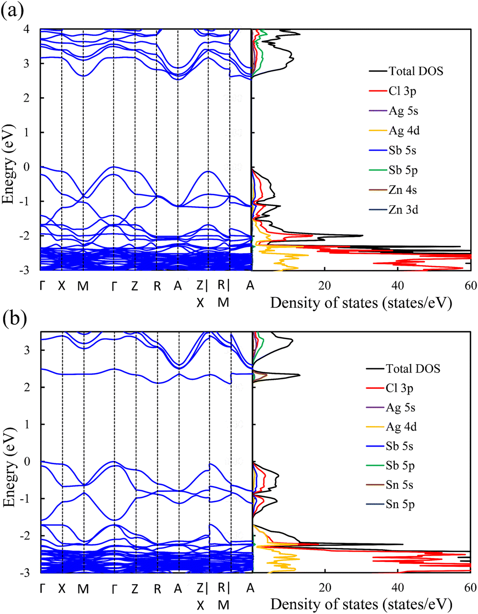
Exploring the electronic structure and bandgap is an important criterion for screening potential photo-absorbers in photovoltaic applications. To describe correctly the electronic properties and the bandgap, we applied the sophisticated HSE hybrid functional while including the SOC effect. Fig. 3a shows the band structure, the total density of states (DOS), and the partial density of states (PDOS) of a pristine Cs2AgSbCl6 conventional cell. The band structure and partial band structure of the pristine Cs2AgSbCl6 primitive cell are shown in Fig. S3 (ESI†). It can be clearly seen from the PDOS in Fig. 3a that the valence band (VB) of the pristine perovskite is as broad as the energy range between the Fermi level and below −3.0 eV (to around −5.0 eV, not shown in Fig. 3a for the sake of simplicity). The VB is mainly composed of the occupied Cl 3p state with hybridization from Sb 5s and Ag 4d states. The conduction band (CB) is constructed from the unoccupied Sb 5p states with a contribution from Ag 5s. Moreover, the Cl 3p states contribute to the CB, which is similar to the case of the other double perovskites.32,45 In the Cs2AgSbCl6 perovskite structure, the Ag–Cl and Sb–Cl bonds are classified as having a transient characteristic.22 However, the orbitals of the Cs cations do not contribute to the top of the VB or the bottom of the CB. The occupied Cs s and p states are narrow and deep lying in the VB, outside the energy range shown in Fig. 3a, indicating the ionic bonding character of the Cs cations.22 For comparison, Fig. 3a displays the band structure of the pristine Cs2AgSbCl6 conventional cell with the k-path that is suggested for the doped perovskites using the SeeK-path tool.55,56 The valence band maximum (VBM) is located at the Gamma (Γ) point while the conduction band minimum (CBM) is formed at the A point due to band folding in the case of the conventional cell. This confirms the indirect bandgap character of the pristine Cs2AgSbCl6 double perovskite.19 In the case of the primitive cell, the band folding disappears and the VBM and CBM are located at the X and L points, respectively (Fig. S3, ESI†).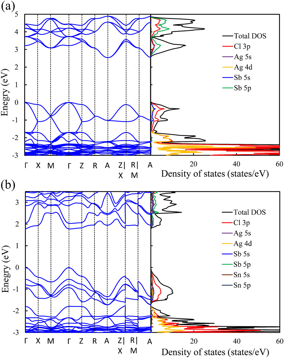 | ||
| Fig. 3 Band structure (left) and density of states (right) of (a) the pristine perovskite and (b) the Sn2+–Sn2+ doped perovskites. | ||
Upon Sn2+–Sn2+ dopant inclusion, as shown in Fig. 3b, the shape of the band structure and the density of states show pronounced changes. The Sb3+ and Sn2+ cations have the same electronic configuration of s2p0. Most important is that the Sn2+ orbitals contribute greatly to the band edges and significantly affect the bandgap character of the doped perovskites. The predominant contribution to the VBM is made by the Sn 5s and Cl 3p states, as shown in Fig. 3b. The strong hybridization at the VBM between the Sn 5s dopant states and the Cl 3p, Ag 4d, and Sb 5s host states widens the VB and hence reduces the bandgap. Moreover, the Sn 5p states and Sb 5p states represent the predominant contribution to the CB. In the case of the Sn2+–Sn2+ doped structure, the VBM is preserved and located at the Γ point, similar to the host perovskite as shown in Fig. 3a. Moreover, the Sn2+ dopant does not introduce deep defect states within the bandgap. Moreover, due to the strong contribution from the Sn orbitals, the location of the CBM is changed and transformed to the Γ point. This increases the CB width and leads to a bandgap reduction and an indirect-to-direct bandgap transition. Therefore, the bandgap transition in doped perovskites could be achieved by adjusting the orbital contribution at the band edges, which can be realized by choosing the appropriate M dopant cation. Interestingly, with the help of ab initio calculations, the process of finding the appropriate M dopant cation can be accelerated. The chemical ordering effect on the electronic properties could be explored using a larger supercell; however, this is not feasible for the computer-resource-intensive HSE + SOC approach used here.
The detailed partial orbital contribution of all the ions to the VBM and the CBM at the k-path in the pristine and Sn2+–Sn2+ doped perovskites is represented by the partial band structure as shown in Fig. 4a and b.57 In the pristine perovskite, the VBM and CBM are localized at the Γ and A symmetry points, respectively (Fig. 4a). The major contribution to the VBM at the Γ point is related to Cl 3p with participation from the Sb 5s and Ag 4d orbitals. At the Γ point, the Ag 5s states do not make a pronounced contribution to the CBM due to the different symmetry.32 By contrast, the hybridization between the Ag 5s and Sb 5p states at the A point leads to a down-shift of the CB and, hence, results in the indirect bandgap character of the pristine Cs2AgSbCl6 perovskite. In the case of the Sn2+–Sn2+ doped system (Fig. 4b), in addition to the contribution from the Cl 3p states to the VBM at the Γ point, the occupied Sn 5s states make a significant contribution to the VBM at this point. This hybridization extends the VB and hence reduces the bandgap, as shown in the density of states (Fig. 3b). In addition, the unoccupied Sn 5p and Sb 5p states are strongly hybridized at the Γ point, and hence the CB is shifted down at the Γ point. Therefore, the CBM is shifted from the A point to the Γ point and an indirect–direct bandgap transition is shown in the Sn2+–Sn2+ doped perovskite.
 | ||
| Fig. 4 Partial band structure of (a) the pristine perovskite, and the (b) Sn2+–Sn2+, (c) Zn2+–Zn2+, and (d) Sn4+–VAg doped perovskites. Color codes are added to show the orbital contributions to the bottom of the CB and the top of the VB. | ||
The electronic configuration of Sn2+ cation is therefore responsible for the bandgap transition in the Sn2+–Sn2+ doped perovskite. In the Sn2+ cation, the s orbitals are fully occupied and located at the top of the VB of the host perovskite, while the p orbitals are empty and lying at the CBM. Other M2+-doped perovskites, i.e., Ge2+–Ge2+, Sn2+–VAg, and Ge2+–VAg, show similar electronic configurations (s2p0) and hence could show similar features to the Sn2+–Sn2+ doped system. Fig. S4 (ESI†) shows the band structure and the density of states of the Ge2+–Ge2+, Sn2+–VAg, and Ge2+–VAg doped perovskites. As shown in Fig. S4 (ESI†), these systems show an indirect–direct bandgap transition with the contribution from Ge2+ and Sn2+ orbitals to the VB and the CB. Fig. S5 (ESI†) shows the partial orbital contributions to the VBM and CBM of these doped perovskites. Similar to Sn2+–Sn2+, although the major contribution to the VBM (Cl 3p states) and the CBM (Sb 5p states) does not change with respect to pristine Cs2AgSbCl6, the s and p orbitals of Ge2+ and Sn2+ significantly participate and hybridize with the host orbitals at the band edges of the doped perovskites, leading to reduced direct bandgaps (Fig. S5, ESI†).
In addition to the bandgap character, the bandgap value is another important criterion in photovoltaic applications. In Table 1 we present the bandgaps for the pristine and all the doped perovskites. The bandgap of the pristine Cs2AgSbCl6 double perovskite obtained from the HSE with SOC calculations is 2.53 eV, which shows a very good correlation with the experimental value of 2.54 eV.19 This confirms the reliability of our computational methods for the calculated bandgaps of the doped structures. In the doped perovskites, the hybridization between the dopant orbitals and the host orbitals extends the band edges and hence reduces the bandgap. Interestingly, the bandgap values of Sn2+–Sn2+ (1.78 eV), Ge2+–Ge2+ (1.80 eV), Sn2+–VAg (1.88 eV) and Ge2+–VAg (1.79 eV) are in the ideal range (1.7–1.9 eV)16 for top cells in tandem devices. Furthermore, the bandgaps of these doped perovskites are close to the theoretically reported mixed lead-free perovskites for the top cell in tandem solar cells.16 However, the bandgap reduction in the doped perovskites is due to the reasonable contribution of the dopant orbitals (s2p0) at the band edges of the host perovskites.
In contrast to the s2p0 doping configurations, Zn2+–Zn2+ doped perovskite with the d10s0 electronic configuration (similar to that of Ag cations) leads to a negligible change in the electronic structure with respect to the pristine perovskite. In this case, as shown in Fig. 5a, the occupied Zn 3d states are lying deep in the VB and do not hybridize with the host orbitals at the VBM, which is described by the Cl 3p and Ag 5d states, as in the case of the pristine perovskite. Moreover, the unoccupied Zn 4s states interact weakly with the Sb 5p and Ag 5s states at the CBM. The hybridization between the Zn s orbitals and the host orbitals leads to the down-shift of the CB at the M point, as shown in Fig. 4c. However, the VBM and the CBM are still located at the Γ point and the A point, respectively, as in the case of the pristine perovskite. Therefore, an indirect bandgap is preserved for the Zn2+–Zn2+ doped perovskite. The weak contribution of the Zn orbitals to the VB and CB resulted in no change of the bandgap (2.53 eV) with respect to pristine Cs2AgSbCl6. Similar behavior is shown in the case of the Cd2+–Cd2+ doped perovskite with the same electronic configuration of d10s0 (Fig. S6a and S5b, ESI†). In addition, we noticed a small contribution from the Cd 5s states to the CBM at the A point, which leads to the down-shift of the CBM and reduces the bandgap to 2.30 eV. However, an indirect band gap is not desirable for photovoltaic applications, but could be suitable for other green energy applications.
 | ||
| Fig. 5 Band structure (left) and density of states (right) of (a) Zn2+–Zn2+ and (b) Sn4+–VAg doped perovskites. | ||
To confirm the role of the dopant oxidation state and hence the electronic configuration on the tunability of the electronic structure, we also calculated the electronic structure of the Sn4+–VAg, and Ge4+–VAg doped perovskites with the electronic configuration of s0p0. Hereby, the p orbitals are unoccupied in addition to the unoccupied s orbitals. Fig. 5b shows that the major contribution to the VBM (Cl 3p states) does not change with respect to pristine Cs2AgSbCl6, and the Sn4+ dopant introduces defect states at the bottom of the CB. Within the electronic configuration of s0p0, the unoccupied Sn 5s states significantly participate in the CBM of the doped Sn4+–VAg perovskite. Moreover, the unoccupied Sn 5p states are located at a high energy in the CB and therefore do not participate at the CBM. With the strong contribution from the unoccupied Sn 5s states, the CBM is further pushed down at the R point compared with the pristine structure, which reduces the bandgap (2.11 eV), as shown in Fig. 4d and Table 1. However, due to the location of the VBM at the Γ point, the bandgap is of indirect character. The Ge4+–VAg doped perovskite shows a similar electronic structure to that of the Sn4+–VAg doped perovskite, as shown in Fig. S5e and S6b (ESI†), with an indirect bandgap of 1.92 eV. Accordingly, the orbital contribution from the occupied s orbitals together with the unoccupied p orbitals at the band edges dominates the indirect–direct bandgap transition and hence the tunability of the electronic structure of the doped perovskites. This confirms the importance of the dopant oxidation state and the electronic configuration on the electronic-structure engineering of double perovskites.
Another important parameter in photovoltaic applications is the effective mass, which is associated with the mobility of electrons and holes. In Table S2 (ESI†) we present the effective mass along the Γ–M path with light carriers, of the proposed Sn2+- and Ge2+-based perovskites. As shown in Table S2 (ESI†), the Sn2+–Sn2+ and Ge2+–Ge2+-doped perovskites have low effective masses that are comparable with the effective masses of MAPbI3;16 therefore, they could have a high mobility for carrier transport. It has been reported that, in semiconducting materials, the CB dominated by cationic p states gives a small electron effective mass.16
3.3. Optical absorption spectra
The optical absorption is related to the performance of perovskite-based solar cells. We calculated the optical absorption coefficients (cm−1) of the pristine and M-doped perovskites using the HSE hybrid functional with the inclusion of the SOC effect. Fig. 6 shows the optical absorption coefficients for all the doped perovskites in comparison with that of the pristine Cs2AgSbCl6 perovskite. From Fig. 6a, we observe that the pristine perovskite shows a single peak in the photon energy range up to 4 eV, which is assigned to the electronic transition from Cl 3p states to Sb 5 p states or Ag 5s states. By contrast, all the doped perovskites with the dopant electronic configuration of s2p0 exhibit multi-peak features in the visible-light energy range, which is attributed to electronic transitions from the VBM states (mainly Cl 3p states and Sn (Ge) 5s states) to the Sn (Ge) 5p states. Therefore, these doped perovskites can absorb light with a longer wavelength and, therefore, the optical absorption ability is higher than that of the pristine perovskite. The presence of these multi-peaks can be attributed to the indirect−direct bandgap transition and is due to the electronic transitions that occur at the Z point and the Z|X point in the first Brillouin zone of the doped perovskites. These transitions are absent in the pristine perovskite, and hence make the doped perovskites potential candidates for photovoltaic cells. Interestingly, the high optical absorption efficiency of these doped perovskites is comparable to that of the MAPbI3 perovskite.16 In addition to the multi-peaks, the main peak is observed up to 4 eV, which is also the location of the main peak of the pristine Cs2AgSbCl6 perovskite.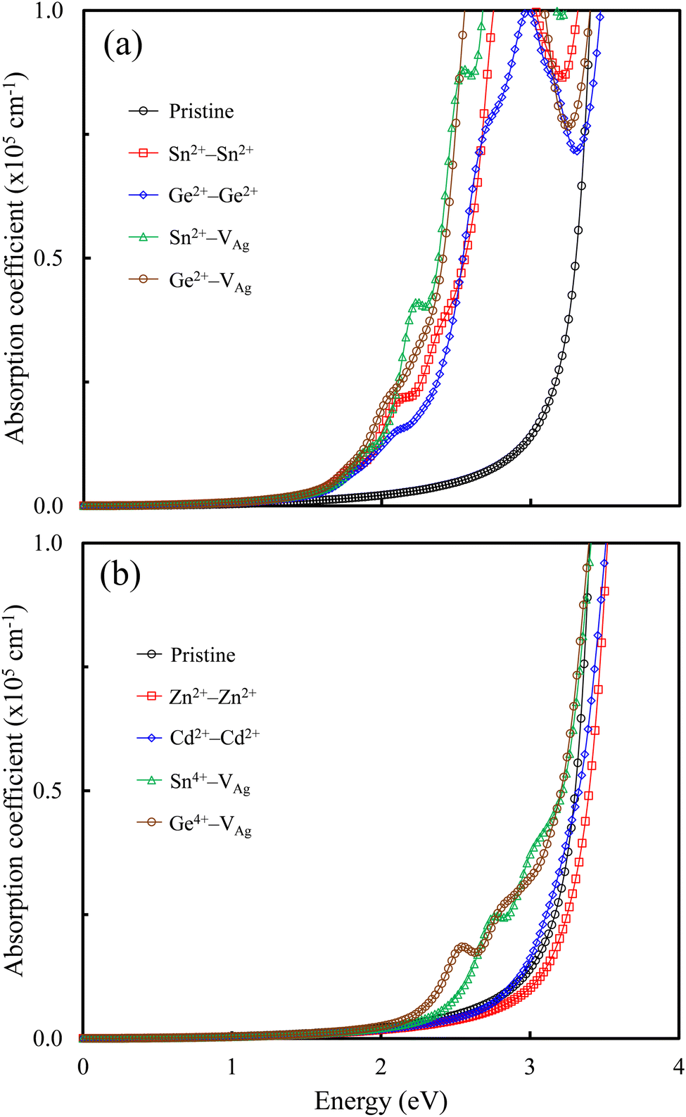 | ||
| Fig. 6 (a and b) Calculated absorption coefficients of the pristine and all doped perovskites. | ||
Fig. 6b shows that the doped perovskites with the dopant electronic configurations of d10s0 and s0p0 have similar optical absorption spectra to that of the pristine perovskite in the energy range up to 4 eV due to the indirect bandgap character. In addition, the Sn4+–VAg and Ge4+–VAg doped perovskites show slightly extended visible-light absorption bands for the optical transitions between the VBM states and the Sn (Ge) 5s states, indicating an improved absorption efficiency over the pristine perovskite due to the reduced bandgaps. Therefore, Fig. 6 shows the effect of the dopant electronic configuration (oxidation state) on the absorption spectra of the doped perovskites, in accordance with the reported electronic properties.
4. Conclusions
In conclusion, we investigated the incorporation of divalent (Sn2+, Ge2+, Zn2+, and Cd2+) and tetravalent (Sn4+and Ge4+) cations at the mixed B-site of the Cs2AgSbCl6 double perovskite using the HSE hybrid functional and the SOC effect. The doped perovskites show good structural and thermodynamic stabilities. Due to the strong contribution from the dopant orbitals (s2p0) at the VBM and the CBM, an indirect–direct bandgap transition has been observed for the doped perovskites with Sn2+and Ge2+ cations. The calculated bandgaps of the doped perovskites are found to be in the ideal bandgap range of 1.70–1.90 eV for use as the top cell in tandem solar cells. By contrast, dopants (Zn2+, Cd2+, Sn4+, and Ge4+) with electronic configurations of d10s0 and s0p0 resulted in a negligible tunability for the electronic structure, and hence show an indirect bandgap character that could be suitable for other energy applications. Therefore, the orbital contribution from the occupied s orbitals together with the unoccupied p orbitals at the band edges dominates the electronic-structure tunability of the doped perovskites. The optical properties of the Sn2+- and Ge2+-based perovskites display a high absorption efficiency and a broad optical absorption spectrum, which make them potential candidates for the future green energy applications. We expect that this study will provide a rational computational guide for exploring potential doped perovskites as photo-absorbers for optoelectronic applications.Conflicts of interest
There are no conflicts to declare.Acknowledgements
This work was supported by the Virtual Engineering Platform Project of the Ministry of Trade, Industry and Energy (MOTIE) of Korea (grant number: N0002599). The calculations were performed using computational resources provided by the High-Performance Computing (HPC) infrastructure of Bibliotheca Alexandrina in Egypt.References
- L. Mao, C. C. Stoumpos and M. G. Kanatzidis, J. Am. Chem. Soc., 2019, 141, 1171–1190 CrossRef CAS PubMed.
- A. Swarnkar, A. R. Marshall, E. M. Sanehira, B. D. Chernomordik, D. T. Moore, J. A. Christians, T. Chakrabarti and J. M. Luther, Science, 2016, 354, 92–95 CrossRef CAS PubMed.
- H. Cho, S.-H. Jeong, M.-H. Park, Y.-H. Kim, C. Wolf, C.-L. Lee, J. H. Heo, A. Sadhanala, N. Myoung, S. Yoo, S. H. Im, R. H. Friend and T.-W. Lee, Science, 2015, 350, 1222–1225 CrossRef CAS PubMed.
- J. Li, L. Xu, T. Wang, J. Song, J. Chen, J. Xue, Y. Dong, B. Cai, Q. Shan, B. Han and H. Zeng, Adv. Mater., 2017, 29, 1603885 CrossRef PubMed.
- NREL. Best Research-Cell Efficiencies, https://www.nrel.gov/pv/cell-efficiency.html (2022).
- Z. Hu, Z. Lin, J. Su, J. Zhang, J. Chang and Y. Hao, Sol. RRL, 2019, 3, 1900304 CrossRef.
- J. Li, H.-L. Cao, W.-B. Jiao, Q. Wang, M. Wei, I. Cantone, J. Lü and A. Abate, Nat. Commun., 2020, 11, 310 CrossRef CAS PubMed.
- M.-G. Ju, J. Dai, L. Ma and X. C. Zeng, J. Am. Chem. Soc., 2017, 139, 8038–8043 CrossRef CAS PubMed.
- T. Jesper Jacobsson, J.-P. Correa-Baena, M. Pazoki, M. Saliba, K. Schenk, M. Grätzel and A. Hagfeldt, Energy Environ. Sci., 2016, 9, 1706–1724 RSC.
- G. E. Eperon, T. Leijtens, K. A. Bush, R. Prasanna, T. Green, J. T.-W. Wang, D. P. McMeekin, G. Volonakis, R. L. Milot, R. May, A. Palmstrom, D. J. Slotcavage, R. A. Belisle, J. B. Patel, E. S. Parrott, R. J. Sutton, W. Ma, F. Moghadam, B. Conings, A. Babayigit, H.-G. Boyen, S. Bent, F. Giustino, L. M. Herz, M. B. Johnston, M. D. McGehee and H. J. Snaith, Science, 2016, 354, 861–865 CrossRef CAS PubMed.
- J. Zhou, X. Rong, M. S. Molokeev, X. Zhang and Z. Xia, J. Mater. Chem. A, 2018, 6, 2346–2352 RSC.
- G. Longo, S. Mahesh, L. R. V. Buizza, A. D. Wright, A. J. Ramadan, M. Abdi-Jalebi, P. K. Nayak, L. M. Herz and H. J. Snaith, ACS Energy Lett., 2020, 5, 2200–2207 CrossRef CAS.
- M. R. Filip, S. Hillman, A. A. Haghighirad, H. J. Snaith and F. Giustino, J. Phys. Chem. Lett., 2016, 7, 2579–2585 CrossRef CAS PubMed.
- A. H. Slavney, L. Leppert, D. Bartesaghi, A. Gold-Parker, M. F. Toney, T. J. Savenije, J. B. Neaton and H. I. Karunadasa, J. Am. Chem. Soc., 2017, 139, 5015–5018 CrossRef CAS PubMed.
- P. Sebastiá-Luna, J. Calbo, N. Albiach-Sebastián, M. Sessolo, F. Palazón, E. Ortí and H. J. Bolink, Chem. Mater., 2021, 33, 8028–8035 CrossRef.
- R. Ali, G.-J. Hou, Z.-G. Zhu, Q.-B. Yan, Q.-R. Zheng and G. Su, J. Mater. Chem. A, 2018, 6, 9220–9227 RSC.
- K. P. Lindquist, S. A. Mack, A. H. Slavney, L. Leppert, A. Gold-Parker, J. F. Stebbins, A. Salleo, M. F. Toney, J. B. Neaton and H. I. Karunadasa, Chem. Sci., 2019, 10, 10620–10628 RSC.
- M. B. Gray, E. T. McClure and P. M. Woodward, J. Mater. Chem. C, 2019, 7, 9686–9689 RSC.
- T. T. Tran, J. R. Panella, J. R. Chamorro, J. R. Morey and T. M. McQueen, Mater. Horiz., 2017, 4, 688–693 RSC.
- E. T. McClure, M. R. Ball, W. Windl and P. M. Woodward, Chem. Mater., 2016, 28, 1348–1354 CrossRef CAS.
- A. Karmakar, M. S. Dodd, S. Agnihotri, E. Ravera and V. K. Michaelis, Chem. Mater., 2018, 30, 8280–8290 CrossRef CAS.
- J. E. F. S. Rodrigues, C. A. Escanhoela, B. Fragoso, G. Sombrio, M. M. Ferrer, C. Álvarez-Galván, M. T. Fernández-Díaz, J. A. Souza, F. F. Ferreira, C. Pecharromán and J. A. Alonso, Ind. Eng. Chem. Res., 2021, 60, 18918–18928 CrossRef CAS.
- A. H. Slavney, L. Leppert, A. Saldivar Valdes, D. Bartesaghi, T. J. Savenije, J. B. Neaton and H. I. Karunadasa, Angew. Chem., Int. Ed., 2018, 57, 12765–12770 CrossRef CAS PubMed.
- Y. Zhou, J. Chen, O. M. Bakr and H.-T. Sun, Chem. Mater., 2018, 30, 6589–6613 CrossRef CAS.
- K. Du, W. Meng, X. Wang, Y. Yan and D. B. Mitzi, Angew. Chem., Int. Ed., 2017, 56, 8158–8162 CrossRef CAS PubMed.
- Q. Sun, J. Wang, W. Yin and Y. Yan, Adv. Mater., 2018, 30, 1705901 CrossRef PubMed.
- Q. Li, Y. Wang, W. Pan, W. Yang, B. Zou, J. Tang and Z. Quan, Angew. Chem., Int. Ed., 2017, 56, 15969–15973 CrossRef CAS PubMed.
- F. Giustino and H. J. Snaith, ACS Energy Lett., 2016, 1, 1233–1240 CrossRef CAS.
- U. H. Hamdeh, B. J. Ryan, R. D. Nelson, M. Zembrzuski, J. Slobidsky, K. J. Prince, I. Cleveland, A. Vela-Ramirez, A. C. Hillier and M. G. Panthani, J. Phys. Chem. Lett., 2019, 10, 3134–3139 CrossRef CAS PubMed.
- D. Manna, T. K. Das and A. Yella, Chem. Mater., 2019, 31, 10063–10070 CrossRef CAS.
- P. Han, C. Luo, W. Zhou, J. Hou, C. Li, D. Zheng and K. Han, J. Phys. Chem. C, 2021, 125, 11743–11749 CrossRef CAS.
- X. Ma, Z. Li and J. Yang, J. Phys. Chem. C, 2021, 125, 10868–10875 CrossRef CAS.
- G. Kresse and J. Furthmüller, Comput. Mater. Sci., 1996, 6, 15–50 CrossRef CAS.
- G. Kresse and J. Furthmüller, Phys. Rev. B: Condens. Matter Mater. Phys., 1996, 54, 11169–11186 CrossRef CAS PubMed.
- P. E. Blöchl, Phys. Rev. B: Condens. Matter Mater. Phys., 1994, 50, 17953–17979 CrossRef PubMed.
- J. P. Perdew, K. Burke and M. Ernzerhof, Phys. Rev. Lett., 1996, 77, 3865–3868 CrossRef CAS PubMed.
- H. J. Monkhorst and J. D. Pack, Phys. Rev. B: Solid State, 1976, 13, 5188–5192 CrossRef.
- F. Birch, Phys. Rev., 1947, 71, 809–824 CrossRef CAS.
- J. Heyd, G. E. Scuseria and M. Ernzerhof, J. Chem. Phys., 2003, 118, 8207–8215 CrossRef CAS.
- J. Heyd, G. E. Scuseria and M. Ernzerhof, J. Chem. Phys., 2006, 124, 219906 CrossRef.
- A. V. Krukau, O. A. Vydrov, A. F. Izmaylov and G. E. Scuseria, J. Chem. Phys., 2006, 125, 224106 CrossRef PubMed.
- M. Gajdoš, K. Hummer, G. Kresse, J. Furthmüller and F. Bechstedt, Phys. Rev. B: Condens. Matter Mater. Phys., 2006, 73, 045112 CrossRef.
- M. Fox, Optical properties of solids, Oxford University Press, Oxford, New York, 2nd edn, 2010 Search PubMed.
- S. Lardhi, D. Noureldine, M. Harb, A. Ziani, L. Cavallo and K. Takanabe, J. Chem. Phys., 2016, 144, 134702 CrossRef PubMed.
- G. Yu, S. Xue, R. Yin, Q. Wu, T. Gao, Y. Song, R. Wang, W. Cong, C. Guan and Y. Lu, Adv. Theory Simul., 2021, 4, 2100142 CrossRef CAS.
- A. Singh, R. Chaurasiya, A. Bheemaraju, J.-S. Chen and S. Satapathi, ACS Appl. Energy Mater., 2022, 5, 3926–3932 CrossRef CAS.
- T. Wang, K. C. Pitike, Y. Yuan, S. M. Nakhmanson, V. Gopalan and B. Jalan, APL Mater., 2016, 4, 126111 CrossRef.
- R. D. Shannon, Acta Crystallogr. Sect. A, 1976, 32, 751–767 CrossRef.
- W. Tang, E. Sanville and G. Henkelman, J. Phys.: Condens. Matter, 2009, 21, 084204 CrossRef CAS PubMed.
- M. Xu, P. Xiao, S. Stauffer, J. Song, G. Henkelman and J. B. Goodenough, Chem. Mater., 2014, 26, 3089–3097 CrossRef CAS.
- V. M. Goldschmidt, Naturwissenschaften, 1926, 14, 477–485 CrossRef CAS.
- R. D. Shannon, Acta Crystallogr. Sect. A, 1976, 32, 751–767 CrossRef.
- M. A. Green, A. Ho-Baillie and H. J. Snaith, Nat. Photonics, 2014, 8, 506–514 CrossRef CAS.
- C. N. Savory, A. Walsh and D. O. Scanlon, ACS Energy Lett., 2016, 1, 949–955 CrossRef CAS PubMed.
- Y. Hinuma, G. Pizzi, Y. Kumagai, F. Oba and I. Tanaka, Comput. Mater. Sci., 2017, 128, 140–184 CrossRef CAS.
- V. Wang, N. Xu, J.-C. Liu, G. Tang and W.-T. Geng, Comput. Phys. Commun., 2021, 267, 108033 CrossRef CAS.
- A. M. Ganose, A. J. Jackson and D. O. Scanlon, J. Open Source Softw., 2018, 3, 717 CrossRef.
Footnote |
| † Electronic supplementary information (ESI) available. See DOI: https://doi.org/10.1039/d2tc02903k |
| This journal is © The Royal Society of Chemistry 2022 |