
Construction of a fully conjugated cross-linked hole-transport film based on ethynyl to enable high mobility for efficient solution-processed OLEDs†
Cancan
Peng
ab,
Hongli
Liu
*ab,
Xinjun
Han
 ab,
Fei
Zhang
ab,
Shirong
Wang
ab and
Xianggao
Li
*ab
ab,
Fei
Zhang
ab,
Shirong
Wang
ab and
Xianggao
Li
*ab
aSchool of Chemical Engineering and Technology, Tianjin University, Tianjin 300072, China
bCollaborative Innovation Center of Chemical Science and Engineering (Tianjin), Tianjin 300072, China. E-mail: liuhongli@tju.edu.cn; lixianggao@tju.edu.cn
First published on 29th August 2022
Abstract
The utilization of cross-linked hole transport layers is deemed as an effective strategy to solve the interlayer miscibility problem in solution-processed organic light-emitting diodes (OLEDs). However, the general incomplete conjugated structure after cross-linking makes it incapable for high hole mobility. In this study, a novel hole transport material N,N′-bis(4-ethynylphenyl)-[1,1′-biphenyl]-4,4′-diamine (E-TPD) with cross-linkable ethynyl groups was designed and synthesized to construct a fully conjugated cross-linked hole transport film. The thermal properties, cross-linking characteristics, photophysical properties, surface morphology, and hole transport ability were studied in detail. The cross-linked E-TPD (p(E-TPD)) film demonstrated a suitable highest occupied molecular orbital (HOMO) energy level, excellent solvent resistance and uniform film morphology. Particularly, its hole mobility reached a high value of up to 8.2 × 10⁻⁴ cm2 V−1 s−1, which is over three times than that of N,N′-di-p-tolyl-N,N′-bis(4-vinylphenyl)-[1,1′-biphenyl]-4,4′-diamine (V-p-TPD) (2.5 × 10⁻⁴ cm2 V−1 s−1) with the same core structure based on cross-linkable vinyl groups. The corresponding solution-processed green phosphorescent OLED gained excellent performance with a turn-on voltage (Von) of 3.3 V, maximum current efficiency (CEmax) of 60.74 cd A−1 and maximum external quantum efficiency (EQEmax) of 17.33%. This study provides a novel tactic to achieve a high-mobility cross-linked hole transport layer by constructing a fully conjugated structure for solution-processed OLEDs.
Introduction
Organic light-emitting diodes (OLEDs) have been widely used in displays and lighting applications due to their wide viewing range, low operating voltage and flexibility.1,2 Owing to the merits of simple operation and high material utilization, solution processes such as spin-coating3–5 and inkjet printing6–8 are the crucial research areas for OLEDs. Interface engineering,9,10 process optimization,11,12 exploring light-emitting materials13,14 and other strategies have been developed to enhance the performance of solution-processed devices. However, interlayer miscibility suffered by the prepared layer due to ugly erosion by the solvent originating from the preparation of upper films is inevitable in solution processes.15,16 To address this issue, the cross-linking strategy has been reported to endow the functional layers with good solvent resistance.17,18 In the preparation of multilayer OLEDs, a cross-linked hole transport layer (HTL) provides a platform to prepare the emitting layer (EML) by the solution method. A series of cross-linkable hole transport materials (HTMs) based on unsaturated acid esters,19–21 oxetane,22–24 benzocyclobutene25 and vinyl26–28 cross-linking groups have been successfully applied in solution-processed OLEDs. However, the cross-linked HTMs generally exhibited low hole mobility (μ) compared with small molecules or conjugated polymers, leading to carrier imbalance in the EML and weakened the device performance.29 Thus, developing cross-linked HTMs with high mobility is an urgent requirement for solution-processed OLEDs.The expanded conjugation backbone of HTMs is effective to improving the intrinsic mobility of the cross-linked hole transport films.30,31 Jou et al.32 synthesized 3,6-bis(4-vinylphenyl)-9-ethylcarbazole (VPEC) with one carbazole as the core and vinyl as the cross-linking group. The reported mobility of this cross-linked VPEC film was 1 × 10⁻⁴ cm2 V−1 s−1. The research group further designed a cross-linkable molecule 9,9′-bis(4-vinylbenzyl)-9H,9′H-3,3′-bicarbazole (VyPyMCz) with two carbazoles in the core33 and its mobility increased to 3.6 × 10⁻⁴ cm2 V−1 s−1 due to the expansion of the conjugation area. The current efficiency (CE) of the green phosphorescent OLED (PHOLED) at 1000 cd m−2 was increased to 51.9 cd A−1 compared with 45.9 cd A−1 of VPEC. Wang et al.34 synthesized V-TPAVTPD and V-TPAVCBP based on the triarylamine structure by the introduction of vinyl bridging groups within the molecule to expand molecular conjugation. Their mobility reached up to 1.1 × 10⁻⁴ and 5.5 × 10⁻⁵ cm2 V−1 s−1, respectively. The CEmax values of the obtained green PHOLEDs were 49.6 and 50.8 cd A−1, respectively. However, the cross-linking groups such as –CH![[double bond, length as m-dash]](https://www.rsc.org/images/entities/char_e001.gif) CH2 in the hole transport molecules generate saturated C–C bonds after polymerization, which isolate each conjugated unit and hence are not conducive to hole transport.35,36
CH2 in the hole transport molecules generate saturated C–C bonds after polymerization, which isolate each conjugated unit and hence are not conducive to hole transport.35,36
The Ethynyl (–C![[triple bond, length as m-dash]](https://www.rsc.org/images/entities/char_e002.gif) C–H) group can maintain the conjugated structure (–CC–) after cross-linking.37 Unfortunately, the reported ethynyl-based HTMs could not form an overall conjugated structure after cross-linking due to the non-integral conjugation of the molecule itself or the non-conjugated units introduced by the cross-linking process, resulting in low mobility and failing to meet the requirements of high-performance devices. Kutonova et al.38 used the rapid reaction of ethynyl with sulfhydryl groups to obtain a highly cross-linked polymer network. Due to the interrupted conjugation by the C–S bond and poor planarity, the hole mobility of the cross-linked film was only 2 × 10⁻⁸ cm2 V−1 s−1. Kang et al.39 reported an ethynyl-based polymer HTM that could be cross-linked to achieve good solvent resistance, but the resultant OLED was endowed with a poor CEmax of 3.2 cd A−1 because of the low mobility caused by the isolated conjugated structure spaced by the C–C bonds.
C–H) group can maintain the conjugated structure (–CC–) after cross-linking.37 Unfortunately, the reported ethynyl-based HTMs could not form an overall conjugated structure after cross-linking due to the non-integral conjugation of the molecule itself or the non-conjugated units introduced by the cross-linking process, resulting in low mobility and failing to meet the requirements of high-performance devices. Kutonova et al.38 used the rapid reaction of ethynyl with sulfhydryl groups to obtain a highly cross-linked polymer network. Due to the interrupted conjugation by the C–S bond and poor planarity, the hole mobility of the cross-linked film was only 2 × 10⁻⁸ cm2 V−1 s−1. Kang et al.39 reported an ethynyl-based polymer HTM that could be cross-linked to achieve good solvent resistance, but the resultant OLED was endowed with a poor CEmax of 3.2 cd A−1 because of the low mobility caused by the isolated conjugated structure spaced by the C–C bonds.
In this regard, a fully conjugated cross-linkable HTM with a conjugated core structure, as well as the ethynyl cross-linking group, is proposed for the first time. Herein, we designed and synthesized a cross-linkable HTM N,N′-bis(4-ethynylphenyl)-[1,1′-biphenyl]-4,4′-diamine (E-TPD) and used ethynyl as the cross-linking group. The triarylamine group associated with ethynyl enabled the formation of a fully conjugated cross-linked hole transport network, realizing an excellent solvent-resistant and high-mobility HTL after cross-linking. In comparison with vinyl-based N,N′-di-p-tolyl-N,N′-bis(4-vinylphenyl)-[1,1′-biphenyl]-4,4′-diamine (V-p-TPD), the thermal, photophysical, and hole-transporting properties and surface morphology of E-TPD were studied in detail. The cross-linked E-TPD (p(E-TPD)) film demonstrated a hole mobility of 8.2 × 10⁻⁴ cm2 V−1 s−1, which is three times higher than that of cross-linked V-p-TPD (p(V-p-TPD), 2.5 × 10⁻⁴ cm2 V−1 s−1). The solution-processed green PHOLED based on p(E-TPD) as the HTL showed a CEmax of 60.74 cd A−1 and maximum external quantum efficiency (EQEmax) of 17.33%.
Experimental section
Materials and methods
The synthetic route of the target product E-TPD is illustrated in Scheme 1. E-TPD was obtained from the Buchwald coupling reaction of N4,N4′-diphenyl-[1,1′-biphenyl]-4,4′-diamine and 1-bromo-4-iodobenzene, followed by the Sonogashira coupling reaction of the product with trimethylsilyl acetylene and the removal of the protecting group. The synthesis details and the structural identification of the compound are provided in the ESI.† V-p-TPD was synthesized according to a previous report.15 All the chemicals used to synthesize the target products were purchased from different reagent companies. PEDOT:PSS (4083) solution, tris[2-(p-tolyl)pyridine]iridium(III) (Ir(mppy)3), tris(4-carbazolyl-9-ylphenyl)amine (TCTA), molybdenum oxide (MoO3), 2,2′,2′′-(1,3,5-benzinetriyl)-tris(1-phenyl-1-H-benzimidazole) (TPBi), and lithium fluoride (LiF) were purchased from Xi'an Polymer Light Technology Corporation. The aluminium pellets were purchased from China Now Metal Materials Technology Co., Ltd.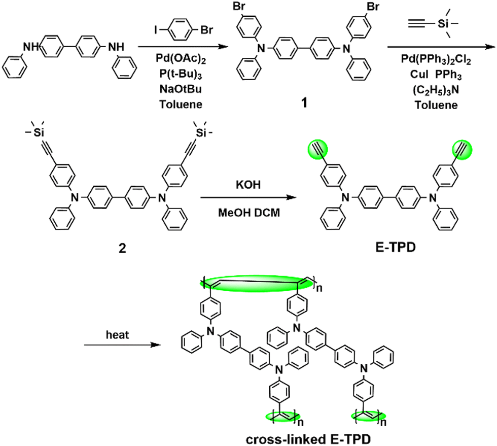 | ||
| Scheme 1 The synthetic route and cross-linking of E-TPD. | ||
Device fabrication
Etched ITO glass substrates were used to fabricate the OLED devices. Before use, the ITO substrates were cleaned ultrasonically with a cleaning agent, distilled water and ethanol for 20 min, respectively, and then treated with oxygen plasma (100 W) for 10 min. PEDOT:PSS was spin-coated (4000 rpm, 30 s) on the ITO substrate and dried at 140 °C for 15 min to form a 30 nm film as the hole injection layer (HIL). The HTMs were dissolved in toluene (5 mg mL−1) and spin-coated (4000 rpm, 30 s) on the HIL. Then, the HTL was cross-linked under respective conditions in an inert atmosphere. The EML comprised of TCTA as the host and Ir(mppy)3 as the guest, which were mixed at a mass ratio of 9![[thin space (1/6-em)]](https://www.rsc.org/images/entities/char_2009.gif) :1. The toluene solution of TCTA and Ir(mppy)3 (10 mg mL−1) was spin-coated (2000 rpm, 30 s) on the HTL and then annealed at 80 °C for 10 min in an inert atmosphere to form a 25 nm film. After these functional layers, TPBi (50 nm), LiF (1 nm) and Aluminium (100 nm) were successively deposited at the rates of 1, 0.1 and 8–12 Å s−1 in a vacuum at pressure under 6 × 10⁻⁴ Pa, respectively.
:1. The toluene solution of TCTA and Ir(mppy)3 (10 mg mL−1) was spin-coated (2000 rpm, 30 s) on the HTL and then annealed at 80 °C for 10 min in an inert atmosphere to form a 25 nm film. After these functional layers, TPBi (50 nm), LiF (1 nm) and Aluminium (100 nm) were successively deposited at the rates of 1, 0.1 and 8–12 Å s−1 in a vacuum at pressure under 6 × 10⁻⁴ Pa, respectively.
For hole only devices, the cleaning of ITO and the preparation of HIL were done the same way as above. The HTMs were dissolved in CHCl3 (30 mg mL−1) and spin-coated (2000 rpm, 30 s) on PEDOT:PSS. Then, the HTLs were cross-linked under respective conditions in a glove box. The cross-linking reaction was performed at 150 °C and 190 °C for 30 min for V-p-TPD and E-TPD, respectively. MoO3 (10 nm) and Al (100 nm) were then sequentially deposited onto the HTL at the rates of 0.2–0.3 Å s−1 and 8–10 Å s−1 in a vacuum at a pressure of 6 × 10⁻⁴ Pa, respectively.
Instruments and measurements
The 1H NMR and 13C NMR spectra were obtained by using a Bruker Avance III HD 400 MHz NanoBAY NMR spectrometer. The mass spectra were measured on a Bruker miorOTOF-QII mass spectrometry. The ultraviolet-visible (UV-vis) absorption spectra were measured by using a Thermo Fisher Scientific GEN10S ultraviolet-visible spectrometer. The photoluminescence (PL) spectra were measured with a FLUOROMAX-4 fluorescence spectrometer. Ultraviolet photoelectron spectroscopy (UPS) was performed on a Thermo Fisher ESCALAB 250Xi spectrometer with a He I light source to get the highest occupied molecular orbital (HOMO) energy level of the HTMs. Ecutoff is the energy of the secondary electron cutoff edge. EHOMO is the energy corresponding to the starting position of the HOMO edge. These were all obtained by the tangent lines in the UPS diagram. TA TGA-Q500 was used to perform the thermogravimetric analysis (TGA) under a N2 atmosphere at a heating rate of 10 °C min−1 from room temperature to 800 °C. The differential scanning calorimetry (DSC) test was carried out on a TA DSC-Q20 under N2 at a heating rate of 10 °C min−1 from room temperature to 300 °C. After the first heating process, the temperature was lowered to room temperature, and a second heating was carried out under the same condition. The data of the two heating processes were recorded. The Fourier transform infrared (FT-IR) spectra were measured by a Nicolet 380 spectrometer. Solid 1H NMR was performed by using an Agilent 600M spectrometer. The surface morphology of the HTM films was observed on a Bruker Dimension icon atomic force microscope (AFM) and S4800 field emission scanning electron microscope (SEM). Alpha Step D300 was used to measure the thickness of the functional layers. The low-temperature phosphorescence spectra were measured using an Edinburgh FLS1000 spectrometer at 77 K with a delay of 1 ms. The performance of the OLEDs was measured using a Keithley 2400 Source Meter and Konicaminolta CS-2000 spectroradiometer.Results and discussion
Thermal properties of HTMs
The thermal properties of E-TPD and V-p-TPD were determined by TGA and DSC. As illustrated in Fig. 1a and b, the E-TPD and V-p-TPD monomers were stable without decomposition at low temperatures. The thermal decomposition temperatures (Td, 5% weight loss) of E-TPD and V-p-TPD were 603 °C and 476 °C, respectively. Their different Td values can be attributed to the structural difference between p(E-TPD) and p(V-p-TPD) generated by the cross-linking of the E-TPD and V-p-TPD monomers at a high temperature. In p(V-p-TPD), each TPD unit was linked by a conjugated double bond, while the C–C single bonds acted as the link between the TPD units in p(V-p-TPD). The C–C bonds in p(V-p-TPD) broke more easily with a further increase in temperature, and thus p(V-p-TPD) decomposed at a lower temperature than p(E-TPD). The rigid structure of p(E-TPD) afforded it a higher Td (603 °C) than that of p(V-p-TPD) (476 °C). The DSC curves of the HTMs are displayed in Fig. 1c and d. During the first scan, both E-TPD and V-p-TPD showed an exothermic process at about 150 °C and 200 °C, respectively, indicating that the cross-linking process occurred.40 No obvious exothermal or endothermal peak was observed during the second heating scan, representing that the full cross-linking of the monomer molecules happened during the first heating process.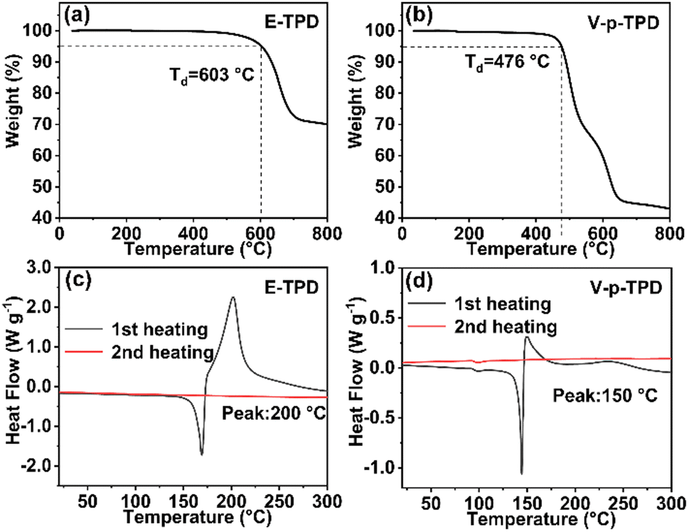 | ||
| Fig. 1 The TGA curves of (a) E-TPD and (b) V-p-TPD. The DSC curves of (c) E-TPD and (d) V-p-TPD. | ||
Cross-linking characteristics of HTMs
In order to determine the solvent resistance of E-TPD, the variation in the UV-vis absorption intensity of the films prepared under different conditions was tested before and after immersion in the solvent. According to previous report,15 V-p-TPD cross-linked by curing at 150 °C for 30 min demonstrated good solvent resistance to several solvents. According to the DSC results, the cross-linking reactions of the E-TPD films were performed at 170, 180 and 190 °C for 30 min. To be consistent with the solvent used for the preparation of EML, toluene was chosen for solvent resistance characterization. The UV-vis absorption spectra of the p(E-TPD) films before and after immersion in toluene for 1 min are demonstrated in Fig. 2a–c. The solvent resistance of the E-TPD films to toluene reached 50%, 80% and 100% after being heated at 170, 180 and 190 °C, respectively. This inferred that the cross-linking reaction of E-TPD was completed at 190 °C.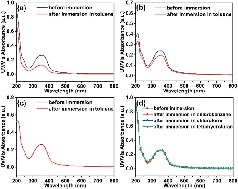 | ||
| Fig. 2 The UV-vis absorption spectra of the p(E-TPD) films heated at (a) 170 °C, (b) 180 °C, and (c) 190 °C before and after immersion in toluene for 1 min. (d) The UV-vis absorption spectra of the p(E-TPD) films heated at 190 °C before and after immersion in different solvents for 1 min. | ||
The resistance of the p(E-TPD) film cross-linked at 190 °C for 30 min towards different solvents was further investigated. As shown in Fig. 2d, the absorption intensity of the p(E-TPD) film remained consistent before and after immersion in chlorobenzene, chloroform and tetrahydrofuran. This indicated that the p(E-TPD) film had the ability of avoiding interlayer miscibility and qualified for the preparation of EMLs by the solution method.
Because the EML was prepared by direct spin-coating on the HTL, the solvent resistance by spin-coating was also investigated, as plotted in Fig. S1 (ESI†). Consistently, the solvent resistance of p(E-TPD) films to toluene reached 100% after heating at 190 °C for 30 min.
FT-IR spectroscopy (Fig. S2, ESI†) revealed that the characteristic peak near 3300 cm−1 corresponding to C–H of the CC–H stretching vibration and the peak near 2100 cm−1 corresponding to the CC stretching vibration disappeared, further confirming the complete cross-linking reaction. In addition, the solid 1H NMR spectra of E-TPD before and after cross-linking are provided in Fig. S3, ESI.† Compared with E-TPD, the content of H located at the low field increased while the content of H located at the high field decreased in p(E-TPD). This corresponds to the disappearance of H at the end of the ethynyl group (at high field: ∼2 ppm) and the generation of H attached to the conjugated polyene (at low field: ∼7 ppm), which implies the occurrence of the cross-linking reaction. Accordingly, the cross-linking mechanism of ethynyl can be regarded as follows: the triple bond is broken into vinyl radicals on heating, and the conjugated polyene structure is formed by addition polymerization.41 After cross-linking of E-TPD, the aromatic units were connected by double bonds to form an overall conjugated structure (Fig. S4, ESI†).
Photophysical properties of HTMs
The photophysical properties of the p(E-TPD) and p(V-p-TPD) films were researched by UV-vis absorption spectroscopy, PL spectra and UPS. The results and related photophysical parameters are plotted and summarized in Fig. 3 and Table 1. As plotted in Fig. 3a and d, the maximum absorption peaks of the p(E-TPD) and p(V-p-TPD) films separately appeared at 362 and 372 nm, respectively, and were related to the n–π* transition of the molecules. The λmax(PL) values of E-TPD and V-p-TPD in film state were 474 and 475 nm, respectively. It can be clearly seen that the PL spectra of E-TPD and V-p-TPD in the film state were significantly redshifted compared with those in solution (Fig. S5, ESI†), which is mainly caused by the existence of weak intermolecular interactions in the solid-state films.42 After cross-linking, the peak positions of E-TPD and V-p-TPD had a red-shift of 6 nm and a blue shift of 3 nm, respectively. Meanwhile, their optical band gap (Eg) calculated from the onset points in the UV-vis absorption spectra also displayed narrowing by 0.08 eV and broadening by 0.02 eV, respectively. These little changes can be ascribed to the larger or smaller conjugate lengths of the materials. The PL peak of V-p-TPD was basically unchanged, while E-TPD exhibited a significant red shift of 66 nm after cross-linking. This is because cross-linking using the ethynyl groups generated a larger conjugated structure with the hole transport unit and enhanced the delocalization of the π-electron.38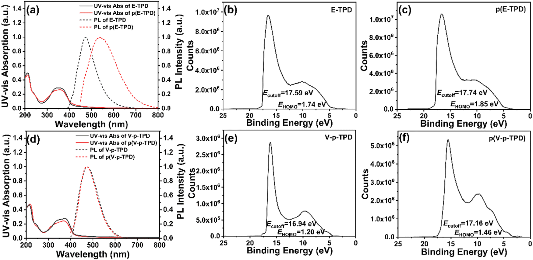 | ||
| Fig. 3 The UV-vis absorption and PL spectra of the (a) E-TPD/p(E-TPD) films and (d) V-p-TPD/p(V-p-TPD) films; the UPS spectra of the (b) E-TPD, (c) p(E-TPD), (e) V-p-TPD and (f) p(V-p-TPD) films. | ||
| Compound | λ max (abs) (nm) | λ max (PL) (nm) | HOMO (eV) | LUMO (eV) | E g (eV) | |
|---|---|---|---|---|---|---|
| E-TPD | Monomer | 356 | 474 | −5.35 | −2.33 | 3.02 |
| Cross-linked | 362 | 540 | −5.32 | −2.38 | 2.94 | |
| V-p-TPD | Monomer | 375 | 475 | −5.45 | −2.52 | 2.93 |
| Cross-linked | 372 | 475 | −5.50 | −2.55 | 2.95 | |
It is crucial to match the HOMO energy levels between the HTM and emitting material to reduce the hole transport barrier. The HOMO and lowest unoccupied molecular orbital (LUMO) electron cloud distribution of the optimized structures of E-TPD and V-p-TPD were calculated by the density functional theory with Gaussian 09 under B3LYP/6-31G(d,p). As revealed in Fig. S6, (ESI†) the HOMO electron clouds in E-TPD and V-p-TPD were basically distributed on the whole molecules, and the energy levels were −4.86 eV and −4.65 eV, respectively. The LUMO electron clouds were distributed over the biphenyl unit and the connected ethynylbenzene or vinylbenzene groups, and the energy levels were −1.10 eV and −1.00 eV, respectively. Their HOMO and LUMO electron cloud distributions overlapped on the biphenyl unit and the connected ethynylbenzene/vinylbenzene groups, which contributed to exciton formation and hole transport.43
Furthermore, the HOMO levels of the E-TPD and V-p-TPD films before and after cross-linking were determined by UPS. As calculated by the Ecutoff and EHOMO of the materials, the HOMO energy levels of the E-TPD and V-p-TPD monomers were −5.35 eV and −5.45 eV (Fig. 3b and e), respectively, and −5.32 eV, −5.50 eV after cross-linking (Fig. 3c and f), respectively. It could be found that the HOMO energy levels of ethynyl-based E-TPD became little shallower after cross-linking, which was attributed to the formation of whole conjugated cross-linked structure. For V-p-TPD, since the vinyl groups turned into saturated C–C single bonds after cross-linking, the hole transport units were separated into disconnected aromatic structures and thus a deeper HOMO energy level was obtained.5 Additionally, since p(E-TPD) featured a larger conjugation and stronger electron delocalization, it demonstrated a shallower HOMO level of −5.32 eV than that of p(V-p-TPD) (−5.50 eV).44,45 Based on the HOMO energy levels and Eg of the materials, the LUMO energy levels were calculated and are listed in Table 1.
The low-temperature (77 K) phosphorescence spectra of the p(E-TPD) and p(V-p-TPD) films are presented in Fig. S7 (ESI†). According to the starting sideband wavelengths of the spectra, the triplet energy levels (ET) of p(E-TPD) and p(V-p-TPD) were calculated to be 2.68 and 2.63 eV, respectively. Both p(E-TPD) and p(V-p-TPD) achieved higher ET than the common green emitters (e.g. Ir(mppy)3, 2.40 eV), which can help in limiting the recombination region within the EML.
The surface morphology of HTLs
The surface morphology of the HTLs before and after cross-linking was observed by AFM, as shown in Fig. 4 and Fig. S8 (ESI†). The root mean square roughness (RMS) values were 0.83 and 1.23 nm for the E-TPD films and 0.78 and 1.12 nm for the V-p-TPD films before and after cross-linking. The roughness of the films increased slightly after cross-linking. Nonetheless, the cross-linking process did not elicit a significant negative effect on the film morphology. Both films exhibited a smooth surface morphology with no obvious pinholes or crazes, as displayed in Fig. S9, (ESI†) demonstrating that they are suitable HTL candidates for OLEDs.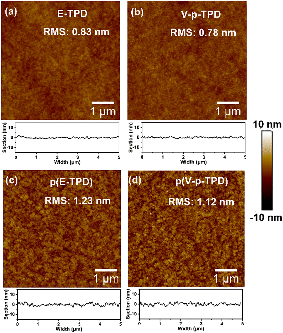 | ||
| Fig. 4 The AFM images of the E-TPD film (a) before and (c) after cross-linking and the V-p-TPD film (b) before and (d) after cross-linking. | ||
Hole-transporting properties of HTLs
Hole only devices (HODs) with the following structure: ITO/PEDOT:PSS (30 nm)/cross-linked HTL (200 nm)/MoO3 (10 nm)/Al (100 nm) were fabricated to test the hole mobility in the films by the space-charge-limited current (SCLC) method. The J–V curve, the fitting curve of ln(J E−2) to E0.5, and the curve of μ vs. the field strength E0.5 of the HODs are depicted in Fig. 5a–c. The hole mobility was calculated by the following formulas:46 | (1) |
 | (2) |
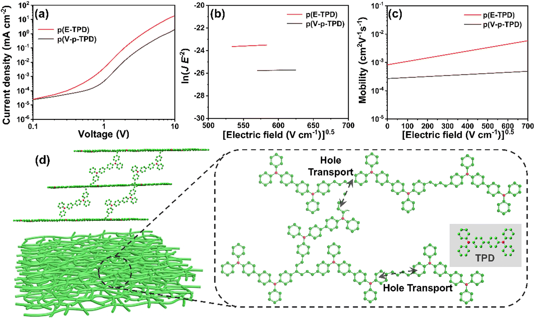 | ||
| Fig. 5 (a) The J–V curves, (b) the fitting curve of ln(J E−2) to E0.5, and (c) the curves of μ vs. the field strength E0.5 of the HODs; (d) the schematic of p(E-TPD) conjugated cross-linked network and hole transport pathway. | ||
The μ0 values of p(E-TPD) and p(V-p-TPD) were calculated to be 8.2 × 10⁻⁴ and 2.5 × 10⁻⁴ cm2 V−1 s−1, respectively. Compared with p(V-p-TPD) that has a similar core structure, p(E-TPD) exhibited a more than three-fold higher μ0. For comparison, the hole mobility of the TPD, E-TPD and V-p-TPD monomers was also investigated, as depicted in Fig. S10 (ESI†). Due to their similar molecular structures, they exhibited similar hole mobility values of 3.2 × 10⁻⁴, 3.6 × 10⁻⁴ and 3.9 × 10⁻⁴ cm2 V−1 S−1, respectively. Notably, compared with the corresponding monomer, p(E-TPD) exhibited higher hole mobility, while p(V-p-TPD) suffered lower hole mobility. This could be because after cross-linking, each hole transport unit in V-p-TPD is isolated by the saturated C–C bond spacing, hindering hole transport.7 While in p(E-TPD), as demonstrated in Fig. 5d, the formation of the fully conjugated cross-linked network amplifies the overlap of electron clouds between the hole transport units, which facilitates hole transfer and then leads to enhanced hole mobility compared with those of the E-TPD monomer and p(V-p-TPD).43,47–49 Fig. S11 (ESI†) reveals that the mobility of the p(E-TPD) films decreased from 7.0 × 10⁻⁴ to 4.5 × 10⁻⁴ cm2 V−1 s−1 after exposure to the air for seven days, indicative of desirable air stability.
Exciton quench experiment
To investigate the effect of the introduction of HTLs on the luminescence performance of the EML (TCTA: 10 wt% Ir(mppy)3), the PL and transient PL spectra of the EMLs without/with HTLs were obtained, as shown in Fig. 6a and b. Almost identical PL peak positions at around 512 nm were sustained in the EMLs without/with HTLs. Additionally, a slight reduction in PL intensity of the EML was observed when E-TPD or V-p-TPD was introduced. The lifetimes (τ) of the EMLs without HTL and with p(E-TPD) and p(V-p-TPD) as the HTL were 1.16, 1.13 and 1.04 μs, respectively. The τ of the EML film with a HTL was shorter than that without a HTL. The reduction in PL intensity and τ can be attributed to exciton quenching at the HTL/EML interface.23 Both PL intensity and TRPL tests indicated that p(E-TPD) brought about less exciton quenching than p(V-p-TPD).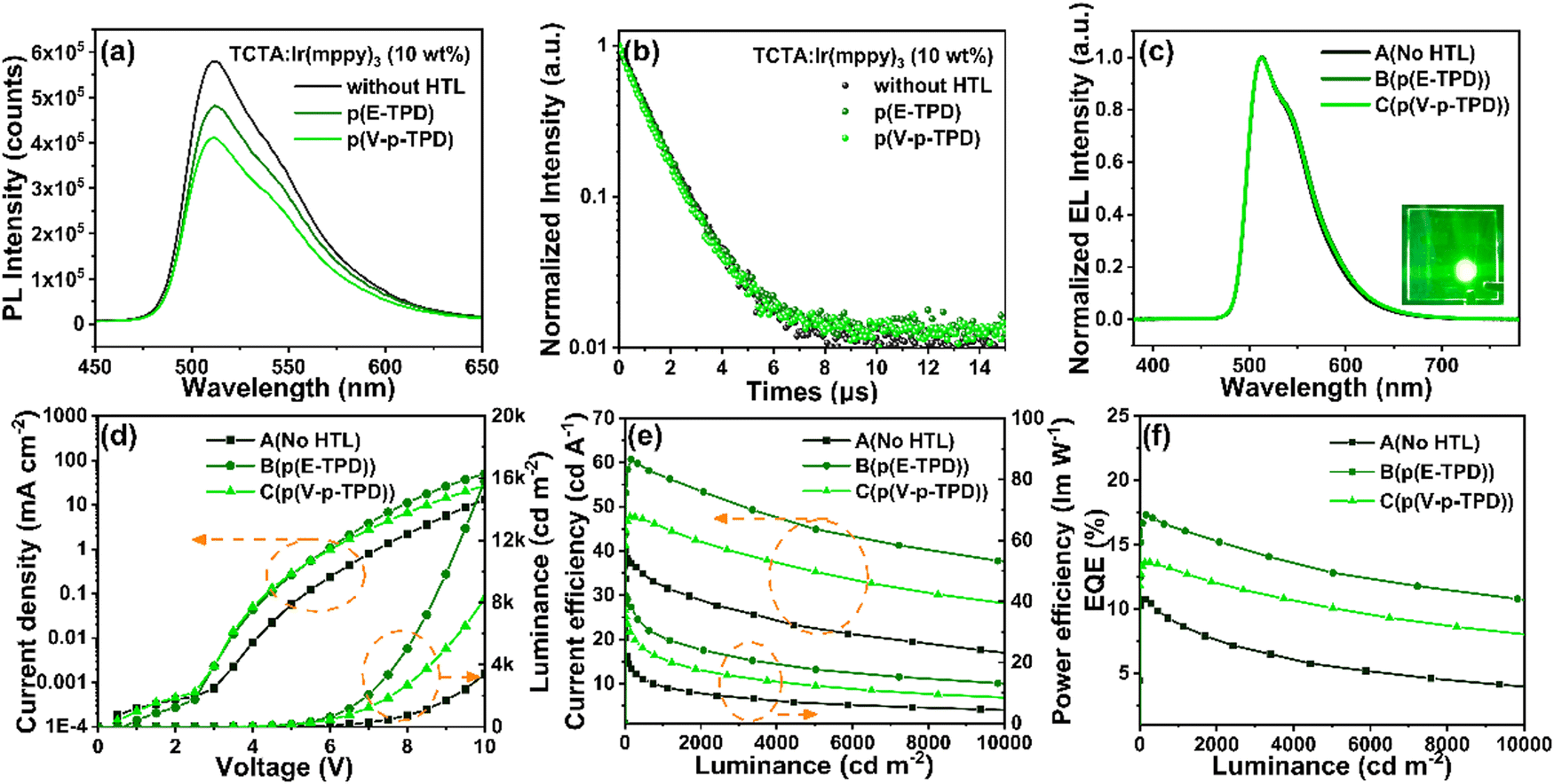 | ||
| Fig. 6 (a) The PL spectra and (b) transient PL spectra of the TCTA: Ir(mppy)3 (10 wt%) films without/with various HTL. (c) The electroluminescence spectra (inset: photo of device electroluminescence), (d) J–V–L curves, (e) CE–L–PE curves and (f) EQE–L curves of the solution-processed green PHOLEDs with the cross-linked HTLs. | ||
Application of cross-linked HTLs in OLEDs
In order to evaluate the application performance of the cross-linked HTLs, solution-processed OLEDs were constructed. According to the HOMO energy levels of p(E-TPD) and p(V-p-TPD), the green phosphorescent material Ir(mppy)3 was chosen as the emitting material, and TCTA with the HOMO energy level at −5.70 eV and LUMO energy level at −2.40 eV was chosen as the host. The structures of the prepared devices were as follows (as shown in Fig. S12, ESI†):A: ITO/PEDOT:PSS (30 nm)/TCTA: Ir(mppy)3 (10 wt%, 25 nm)/TPBi (50 nm)/LiF (1 nm)/Al (100 nm)
B: ITO/PEDOT:PSS (30 nm)/p(E-TPD) (15 nm)/TCTA: Ir(mppy)3 (10 wt%, 25 nm)/TPBi (50 nm)/LiF (1 nm)/Al (100 nm)
C: ITO/PEDOT:PSS (30 nm)/p(V-p-TPD) (15 nm)/TCTA: Ir(mppy)3 (10 wt%, 25 nm)/TPBi (50 nm)/LiF (1 nm)/Al (100 nm)
The characteristic curves of the solution-processed green PHOLEDs with the cross-linked HTLs are shown in Fig. 6c–f, and the device performance are weare summarized in Table 2. The electroluminescence (EL) peaks of all devices were located at 512 nm, which is consistent with the PL peaks and indicated that the excitons recombined in the EML. The devices constructed using p(E-TPD) and p(V-p-TPD) as the HTLs exhibited greater brightness compared with device A. The turn-on voltages (Von) of device B and C were 3.3 and 3.4 V, respectively, which are lower compared with that of device A (3.8 V). This could be because the introduction of HTL facilitated the smoothing of the energy levels between the HIL and EML, reducing the hole injection barrier. Device B exhibited desirable performance with a CEmax of 60.74 cd A−1, maximum power efficiency (PEmax) of 41.74 lm W−1 and EQEmax of 17.33%. This must be credited to the matched HOMO energy level and higher hole mobility of p(E-TPD), which are conducive to promoting injection and carrier balance in the device. At the brightness of 1000 cd m−2, the CE of device B remained at 56.64 cd A−1, suggesting a slight efficiency roll-off.
| Device | V on (V) | L max (cd m−2) | CEmax (cd A−1) | PEmax (lm W−1) | EQEmax (%) | λ EL (nm) | CIE (x,y) (7 V) |
|---|---|---|---|---|---|---|---|
| A(No HTL) | 3.8 | 22239 | 39.87 | 21.30 | 10.22 | 512 | (0.29,0.63) |
| B(p(E-TPD)) | 3.3 | 36630 | 60.74 | 41.74 | 17.33 | 512 | (0.29,0.63) |
| C(p(V-p-TPD)) | 3.4 | 33436 | 47.76 | 37.04 | 13.62 | 512 | (0.29,0.63) |
In addition, the devices with uncross-linked E-TPD and V-p-TPD as the HTL were also prepared. The device characteristics are shown in Fig. S13 and Table S1 (ESI†). Compared with those containing the cross-linked HTLs, luminescence properties of these devices were reduced, which can be attributed to the non-radiative recombination of excitons due to the interlayer miscibility problem. This further confirms the necessity of this cross-linking strategy in the preparation of solution-processed OLEDs.
Conclusions
In this study, we designed and synthesized ethynyl-based cross-linkable HTM E-TPD to obtain a fully conjugated structure after the thermal cross-linking reaction. The material demonstrated an appropriate HOMO energy level, excellent thermal stability and uniform film morphology. Due to the formation of the overall conjugated cross-linked network, the p(E-TPD) film demonstrated a high mobility of 8.2 × 10⁻⁴ cm2 V−1 s−1, which is three times higher than that of vinyl-based p(V-p-TPD) with a similar core structure. The solution-processed green PHOLEDs with conjugated p(E-TPD) showed excellent performance with a Von of 3.3 V, CEmax of 60.74 cd A−1 and EQEmax of 17.33%. The device performance reported here is at a high level among the reported solution-processed green PHOLEDs based on cross-linked HTLs. The construction of such a fully conjugated cross-linked network paves a new path for improving mobility in cross-linked HTMs and the performance of solution-processed OLEDs.Conflicts of interest
There are no conflicts to declare.Acknowledgements
This work was supported by the National Key Research and Development Program of China (2020YFB0408003), the National Natural Science Foundation of China (No. 52173180), the Key Research and Development Project of Tianjin (19ZXNCGX00020), and the S&T Program of Hebei Province (20311401D).Notes and references
- J. W. Park, D. C. Shin and S. H. Park, Semicond. Sci. Technol., 2011, 26, 034002 CrossRef.
- H.-W. Chen, J.-H. Lee, B.-Y. Lin, S. Chen and S.-T. Wu, Light: Sci. Appl., 2018, 7, 17168 CrossRef CAS PubMed.
- V. Gopalan Sree, C. Bathula, H.-K. Youi, H.-S. Kim, J. Inn Sohn and H. Im, J. Mol. Liq., 2021, 338, 116708 CrossRef CAS.
- Y. E. Kim, A. Ko, H. J. Jang, S. J. Yoon, S. H. Roh, J. Y. Lee, J. Y. Lee, D. Kim, J. K. Kim and K. S. Yook, Dyes Pigm., 2021, 187, 109122 CrossRef CAS.
- J. Zhang, H. Liu, X. Li and S. Wang, Org. Electron., 2021, 99, 106334 CrossRef CAS.
- D. G. Yoon, Y. J. Kang, R. Bail and B. D. Chin, J. Inf. Disp., 2021, 22, 91–98 CrossRef CAS.
- Y. Pan, H. Liu, S. Wang, X. Han and X. Li, J. Mater. Chem. C, 2021, 9, 12712–12719 RSC.
- L. Wu, Z. Dong, F. Li, H. Zhou and Y. Song, Adv. Opt. Mater., 2016, 4, 1915–1932 CrossRef CAS.
- J. Wang, L. X. Fan, Y. Z. Wang, Y. C. Wang, Y. Qin, R. Q. Li, Y. H. Chen, Y. Yan, W. Y. Lai, X. W. Zhang and W. Huang, Adv. Mater. Interfaces, 2021, 8, 2100794 CrossRef CAS.
- F. Huang, H. Liu, X. Li and S. Wang, Nano Energy, 2020, 78, 105399 CrossRef CAS.
- L. Zhou, L. Yang, M. Yu, Y. Jiang, C. F. Liu, W. Y. Lai and W. Huang, ACS Appl. Mater. Interfaces, 2017, 9, 40533–40540 CrossRef CAS PubMed.
- L. Zhou, M. Yu, X. Chen, S. Nie, W.-Y. Lai, W. Su, Z. Cui and W. Huang, Adv. Funct. Mater., 2018, 28, 1705955 CrossRef.
- Y. Yu, H. Xing, D. Liu, M. Zhao, H. H. Sung, I. D. Williams, J. W. Y. Lam, G. Xie, Z. Zhao and B. Z. Tang, Angew. Chem., Int. Ed., 2022, 61, e202204279 CAS.
- X. Chen, S. Wang, H. L. Lee, J. Y. Lee, X. Liao, L. Li, W. Zhu and Y. Wang, Adv. Opt. Mater., 2021, 9, 2101518 CrossRef CAS.
- Y. Zhang, X. Wang, X. Li, S. Wang, Y. Pan, Z. Zhong, L. Ying and Y. Xiao, Org. Electron., 2018, 57, 345–351 CrossRef CAS.
- T. Huang, W. Jiang and L. Duan, J. Mater. Chem. C, 2018, 6, 5577–5596 RSC.
- J. H. Lee, C. H. Jeong, M. Godumala, C. Y. Kim, H. J. Kim, J. H. Hwang, Y. W. Kim, D. H. Choi, M. J. Cho and D. H. Choi, J. Mater. Chem. C, 2020, 8, 4572–4579 RSC.
- P. Tang, L. Xie, X. Xiong, C. Wei, W. Zhao, M. Chen, J. Zhuang, W. Su and Z. Cui, ACS Appl. Mater. Interfaces, 2020, 12, 13087–13095 CrossRef CAS PubMed.
- M. Bender, K. M. Schelkle, N. Juergensen, S. Schmid, G. Hernandez-Sosa and U. H. F. Bunz, Macromolecules, 2016, 49, 2957–2961 CrossRef CAS.
- L. Derue, S. Olivier, D. Tondelier, T. Maindron, B. Geffroy and E. Ishow, ACS Appl. Mater. Interfaces, 2016, 8, 16207–16217 CrossRef CAS.
- W. Sun, L. Xie, X. Guo, W. Su and Q. Zhang, ACS Appl. Mater. Interfaces, 2020, 12, 58369–58377 CrossRef CAS.
- M. Hempe, J. Paschek, J. Schelter, A. Umbach, K. Meerholz and M. Reggelin, ChemPlusChem, 2020, 85, 151–158 CrossRef CAS.
- K. W. Tsai, M. K. Hung, Y. H. Mao and S. A. Chen, Adv. Funct. Mater., 2019, 29, 1901025 CrossRef.
- G. Liaptsis and K. Meerholz, Adv. Funct. Mater., 2013, 23, 359–365 CrossRef CAS.
- C. H. Jeong, M. Godumala, J. Yoon, S. Choi, Y. W. Kim, D. H. Choi, M. J. Cho and D. H. Choi, ACS Appl. Mater. Interfaces, 2019, 11, 17602–17609 CrossRef CAS PubMed.
- H. Ha, Y. J. Shim, D. H. Lee, E. Y. Park, I. H. Lee, S. K. Yoon and M. C. Suh, ACS Appl. Mater. Interfaces, 2021, 13, 21954–21963 CrossRef CAS PubMed.
- A. Babaei, K. Rakstys, S. Guelen, V. Fallah Hamidabadi, M.-G. La-Placa, L. Martinez-Sarti, M. Sessolo, H. A. Joel, O. P. M. Gaudin, V. Schanen, M. K. Nazeeruddin and H. J. Bolink, RSC Adv., 2018, 8, 35719–35723 RSC.
- W. Jiang, X. Ban, M. Ye, Y. Sun, L. Duan and Y. Qiu, J. Mater. Chem. C, 2015, 3, 243–246 RSC.
- S. Shahnawaz, S. Sudheendran Swayamprabha, M. R. Nagar, R. A. K. Yadav, S. Gull, D. K. Dubey and J.-H. Jou, J. Mater. Chem. C, 2019, 7, 7144–7158 RSC.
- W. Hu, Z. Zhang, J. Cui, W. Shen, M. Li and R. He, Nanoscale, 2017, 9, 12916–12924 RSC.
- W. M. Zhang, J. Smith, R. Hamilton, M. Heeney, J. Kirkpatrick, K. Song, S. E. Watkins, T. Anthopoulos and I. McCulloch, J. Am. Chem. Soc., 2009, 131, 10814–10815 CrossRef CAS PubMed.
- J.-H. Jou, T.-H. Li, S. Kumar, C.-C. An, A. Agrawal, S.-Z. Chen, P.-H. Fang, G. Krucaite, S. Grigalevicius, J. Grazulevicius and C.-F. Sung, Org. Electron., 2015, 24, 254–262 CrossRef CAS.
- D. K. Dubey, S. S. Swayamprabha, R. A. K. Yadav, D. Tavgeniene, D. Volyniuk, S. Grigalevicius and J.-H. Jou, Org. Electron., 2019, 73, 94–101 CrossRef CAS.
- J. Wang, H. Liu, S. Wu, Y. Jia, H. Yu, X. Li and S. Wang, Chem. Eng. J., 2020, 391, 123479 CrossRef CAS.
- C.-Y. Lin, Y.-C. Lin, W.-Y. Hung, K.-T. Wong, R. C. Kwong, S. C. Xia, Y.-H. Chen and C.-I. Wu, J. Mater. Chem., 2009, 19, 3618–3623 RSC.
- D. He, X. Du, W. Zhang, Z. Xiao and L. Ding, J. Mater. Chem. A, 2013, 1, 4589 RSC.
- Y. Liu, A. Qin and B. Z. Tang, Prog. Polym. Sci., 2018, 78, 92–138 CrossRef CAS.
- K. Kutonova, B. Ebenhoch, L. G. von Reventlow, S. Heissler, L. Rothmann, S. Braese and A. Colsmann, J. Mater. Chem. C, 2020, 8, 16498–16505 RSC.
- B.-G. Kang, H. Kang, N.-G. Kang, C.-L. Lee, K. Lee and J.-S. Lee, Polym. Chem., 2013, 4, 969–977 RSC.
- S. Ameen, J. Lee, H. Han, M. C. Suh and C. Lee, RSC Adv., 2016, 6, 33212–33220 RSC.
- X. Fang, X. Xie, C. D. Simone, M. P. B. Stevens and D. A. Scola, Macromolecules, 2000, 33, 1671–1681 CrossRef CAS.
- C. S. Wu, S. W. Fang and Y. Chen, Phys. Chem. Chem. Phys., 2013, 15, 15121–15127 RSC.
- F. Zhang, S. Wang, H. Zhu, X. Liu, H. Liu, X. Li, Y. Xiao, S. M. Zakeeruddin and M. Gratzel, ACS Energy Lett., 2018, 3, 1145–1152 CrossRef CAS.
- X. Zhao, S. Wang, J. You, Y. Zhang and X. Li, J. Mater. Chem. C, 2015, 3, 11377–11384 RSC.
- F. Zhang, X. Zhao, C. Yi, D. Bi, X. Bi, P. Wei, X. Liu, S. Wang, X. Li, S. M. Zakeeruddin and M. Grätzel, Dyes Pigm., 2017, 136, 273–277 CrossRef CAS.
- D. M. Taylor, IEEE Trans. Dielectr. Electr. Insul., 2006, 13, 1063–1073 CAS.
- F. Zhang, Z. Wang, H. Zhu, N. Pellet, J. Luo, C. Yi, X. Liu, H. Liu, S. Wang, X. Li, Y. Xiao, S. M. Zakeeruddin, D. Bi and M. Grätzel, Nano Energy, 2017, 41, 469–475 CrossRef CAS.
- Y. Wu, Y. Zhao and Y. Liu, Acc. Mater. Res., 2021, 2, 1047–1058 CrossRef CAS.
- T. Niu, W. Zhu, Y. Zhang, Q. Xue, X. Jiao, Z. Wang, Y.-M. Xie, P. Li, R. Chen, F. Huang, Y. Li, H.-L. Yip and Y. Cao, Joule, 2021, 5, 249–269 CrossRef CAS.
Footnote |
| † Electronic supplementary information (ESI) available. See DOI: https://doi.org/10.1039/d2tc02379b |
| This journal is © The Royal Society of Chemistry 2022 |