DOI:
10.1039/D2TC02180C
(Paper)
J. Mater. Chem. C, 2022,
10, 14444-14452
Preferential zinc sputtering during the growth of aluminum doped zinc oxide thin films by radio frequency magnetron sputtering†
Received
25th May 2022
, Accepted 15th August 2022
First published on 16th August 2022
Abstract
Aluminum doped ZnO is one of the main candidates to replace indium tin oxide used as a transparent conducting oxide. Despite the intensive research, the mechanism behind the poor thin-film-resistivity uniformity over the sample deposited by magnetron sputtering is not completely understood. Several independent reports correlate the mirroring of an erosion track on the substrate with energetic negative oxygen ions. However, their role on assisting the thin film growth is not known. In this work, the physical and chemical properties of aluminum doped ZnO are measured with a high spatial resolution at different thin film deposition pressures. The results show that Zn depletion by energetic negative oxygen ion re-sputtering is the main factor correlating with the resistivity and the band gap energy profiles of the deposited films.
1. Introduction
Transparent conducting oxides (TCOs) are essential thin films for solar cells, touch panels, organic light emitting diodes and smart windows.1–3 Recent applications also include plasmonics,4 electron transport layers,5 gas sensors6 and optical spacers.7 This large market comes with high demands for the fabrication cost, throughput, and availability of raw materials. So far, indium tin oxide (ITO) deposited by magnetron sputtering provides a resistivity below 2 × 10⁻⁴ Ω cm and an average transmittance of above 80%, which makes it the most used TCO.1 However, the limited availability of indium, coupled with its intensive use, requires a timely replacement. ZnO is an n-type semiconductor that can reach resistivities below 10−3 Ω cm by doping with several elements, among which Al is regarded as a very promising dopant being one of the most abundant metals. While aluminum doped zinc oxide (AZO) with resistivities below 1 × 10⁻³ Ω cm has been reported by several research groups,8–21 the main problem stands on the limited area (smaller than the sputtering target) were such vales have been measured, which most of the times is near the edge of the substrate. A schematic cross section of a circular magnetron sputtering head is shown in Fig. 1(a) including the set of permanent magnets placed behind the target, the high-density plasma of a torus shape, and the substrate facing the target in a parallel configuration. The magnetic field increases the collision probability of electrons with the neutral gas, elevating considerably the plasma density, with a direct impact on the sputtering rate. This particular geometry results in a very well-defined erosion track on the target surface, which is adjacent to the high-density plasma torus. AZO targets are conductive enough to sustain direct current (DC), pulsed DC, medium-frequency, radio-frequency (RF), or high-power impulse operation modes.22 Electrons and ions form a quasi-neural plasma in the space between the negatively biased target (cathode) and the ground (anode) except for the cathode, anode and substrate sheaths. The cathode sheath thickness and the voltage-drop across it, with respect to plasma potential, depend on the operation mode, besides the other main parameters such as the plasma density and target material.22 The anode sheath is also influenced by various factors, including the magnetron configuration, operation mode, proximity to targets and surface conditions. A sheath can also form in front of the substrate depending on its bias. The needed oxygen can be embedded in the target (oxide target) or supplied in the gas phase for metallic targets (reactive sputtering). Despite a lower cost for metallic targets, the complex control of the reactive process and contamination issues associated with Zn favors AZO deposition from oxide targets.2 DC and RF operation modes are essentially different when taking into account the discharge mechanism.9,22 However, in both cases, the high flux of positive ions impinging on the target at the erosion track releases low-energy secondary electrons that can easily form negative oxygen ions (by electron attachment) to be then accelerated towards the substrate by the cathode sheath.23–25 The correlation between the spatial distribution of the resistivity with the erosion track on the target surface was reported more than three decades ago and is believed to be attributed to two main factors: 1) the role of energetic negative oxygen ions9 and 2) atomic oxygen.3 The first assumption was verified rather recently by Bikowski et al.26 Moreover, it was also reported that the negative oxygen ions reach higher energies in DC than those in RF at 13.56 MHz with a trend of further decreasing energies by RF excitation at even higher frequencies such as 27.12 MHz.26 As far as it is known, there is yet no direct evidence correlating the resistivity with atomic oxygen. Metal oxide thin films deposited by magnetron sputtering are widely used in various applications including thin film transistors, energy devices and sensors where uniformity is a critical parameter.27,28 This underlines the importance to know the role of negative oxygen ions during the thin film growth of metal oxides. This issue was reviewed by Ellmer et al. including several options to diminish the influence of negative ions.29 When depositing AZO by DC magnetron sputtering using Ar, Kr, and Xe, Sato et al. attributed the enhanced degradation observed for Kr and Xe with possible preferential Zn re-sputtering.30 However, Ar is the preferred choice for TCO deposition. In two very recent publications, Stamate reported AZO resistivity variations larger than two orders of magnitude for a span on the substrate of less than 10 mm31 and demonstrated the possibility to reduce the detrimental role of negative ions by reducing their energy with a tuning electrode (TE)32 as schematically presented in Fig. 1(b). Moreover, the spatial distribution of plasma parameters resolved with a dual, electrostatic-thermal probe revealed no direct correlation between the erosion track and plasma density, electron temperature and plasma potential.33 Stamate found it of high relevance that the narrow range of a low DC self-bias that ensures a minimum energy for negative ions corresponds to a transition region from a plume-like plasma discharge to the normal magnetron sputtering operation as presented in Fig. 1(c) where the DC self-bias as function of pressure is presented with and without the TE.32,33 Very recently, it was demonstrated that gallium doped zinc oxide and ITO exhibit the same dependence of the self-bias with pressures as reported for AZO; however, only AZO exhibited the most noticeable correlation of the optoelectronic properties with the erosion track.34 The optoelectronic and analytical properties of AZO thin films by sputtering have been intensively studied by X-ray photoelectron spectroscopy (XPS),35–38 X-ray diffraction (XRD)35,38–41 and Raman spectroscopy36,39 for various parameters (e.g., pressure,42–44 power,45–47 target to substrate distance,31,48 substrate material,49 oxygen gas fraction,50,51 substrate temperature,38 plasma excitation mode,18,52,53 annealing temperature,54,55 target erosion,16 and Al doping fraction56). However, so far, no conclusive correlation has been reported between the role of negative oxygen ions and the physical and chemical properties of AZO thin films as to be able to obtain resistivities below 10−3 Ω cm for a deposited area comparable with that of the target. This work presents the spatially resolved physical and chemical parameters of AZO thin films deposited by radio-frequency magnetron sputtering using an oxide target with the aim of understanding the link between the intrinsic particularities of the magnetron sputtering discharge and the AZO thin film properties.
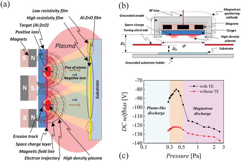 |
| | Fig. 1 (a) Schematic cross section of a circular magnetron sputtering head. (b) Geometric details on the target, tuning-electrode and substrate arrangement. (c) Typical DC self-bias dependence on pressures with and without the tuning-electrode measured with an AZO target for 30 W RF power. | |
2. Experimental section
Materials
The AZO sputtering target (2 inch in diameter, 2% Al2O3 to 98% ZnO by weight) was supplied by Kurt Lesker (Jefferson Hills, USA). The AZO thin films were deposited on 10 × 50 mm2 soda lime glass substrates (0.5 mm in thickness) cut from 100 × 100 mm2 plates provided by Semiconductor Wafer, Inc. (Hsinchu, Taiwan). Up to 8 samples were placed on a large substrate holder that allowed the rotation exposure to the cathode, without breaking the vacuum or turning off the plasma discharge. A certain positioning of the large plate accommodating the TE was used as a shutter during the time needed for the small adjustments of the deposition parameters.34 All samples were deposited at a 30 W RF power for 30 min. There was no intentional heating of the substrate except for the mild effect of plasma exposure (below 50 °C).
Thin film deposition
The AZO target was mounted using a TORUS® magnetron sputtering cathode (Kurt Lesker, Jefferson Hills, USA) with a balanced magnetic field configuration. Following prior optimization, the target-to-substrate distance (see D1 in Fig. 1(b)) was kept at 35 mm and the tuning-electrode-to-substrate distance (see D2 in Fig. 1(b)) was kept at 10 mm, for a TE opening, Φ = 60 mm.
Opto-electronic characterization
The sheet resistance was measured using a custom-made system and a commercial system (KSR-4, Everbeing Int’l Corp., Hsinchu, Taiwan). The custom-made system consisted of two pads distributed perpendicular to the sample length for providing a uniform current and two pins for measuring the drop voltage. The film thickness was measured using a Filmetrics 20 instrument (KLA Co, San Diego, USA). The transmittance spectra were recorded using a Cary 100 UV-VIS spectrometer from Agilent (Victoria, Australia).
TOF-SIMS
A TOF-SIMS IV (ION-TOF GmbH, Münster, Germany) was employed to analyze the samples. 25 ns Pulses of 25 keV Bi+ (primary ions) were arranged to form ion packets with a nominal temporal extent of <0.9 ns at a repetition rate of 10 kHz, yielding a target current of 0.8 pA. These primary ion conditions were used to obtain ion images on 50 × 6 mm2 surface areas (512 × 64 pixels, 1 scan). For all analyses, the electron bombardment (20 eV) was used to minimize the charge build-up at the surface. Desorbed secondary ions were accelerated to 2 keV, mass analyzed in the flight tube, and post-accelerated to 10 keV before detection. The line profiles were extracted from the ion images.
XPS
An ESCALAB XI+ X-ray photoelectron spectrometer microprobe (Thermo Fisher Scientific, East Grinstead, UK) was employed to analyze the samples. A monochromatic Al-Kα X-ray source with a 650 μm spot size and a take-off angle of 90° from the surface plane was used. Atomic concentrations were determined from survey spectra (0–1300 eV, 100 eV detector pass energy, 1 eV step size, 50 ms dwell time, and 2 scans) and were calculated by determining the relevant integral peak intensities using a Smart type background. High-resolution Zn-2p3/2 and O-1s spectra were recorded (25 eV detector pass energy, 0.1 eV step size, 50 ms dwell time, and 2 scans) and the Thermo Fisher Scientific Avantage software (version 5.979, build 06465) was employed for peak fitting, using a Smart type background, a full width at half maximum (FWHM) of 1.5 eV, and a Gauss/Lorentz mix value of 70%. A spectrum was acquired each 0.5 mm along the entire sample corresponding to 100 surface locations.
XRD
Crystallographic mapping of the orientation of the deposited AZO layer was performed by X-ray diffraction using a Rigaku SmartLab diffractometer in the Bragg–Brentano configuration (Cu–Kα radiation). Using a x/y translation stage, the 50 × 50 mm2 AZO samples were mapped with a resolution of 4 × 4 mm2 using a 5 × 5 mm2 beam size controlled by a motorized divergence slit on the incoming X-ray beam. The 100, 200 and 110 reflections were fitted using a Pseudo Voigt function, determining the position, intensity and FWHM of the reflections. The 2D crystal structure analysis of the AZO thin films was performed via X-ray diffraction (Tokyo, Japan), Bragg–Brentano geometry, Cu–Kα radiation, 10–90° in 2θ and 0.02 step size degrees.
3. Results and discussion
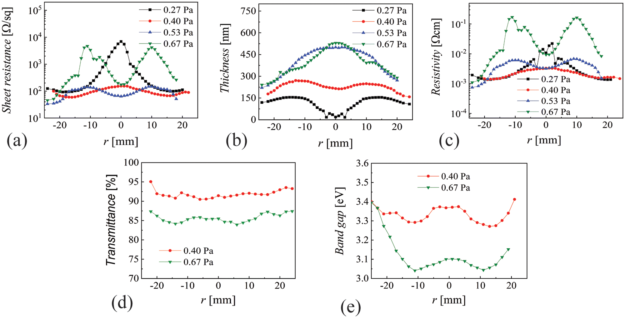
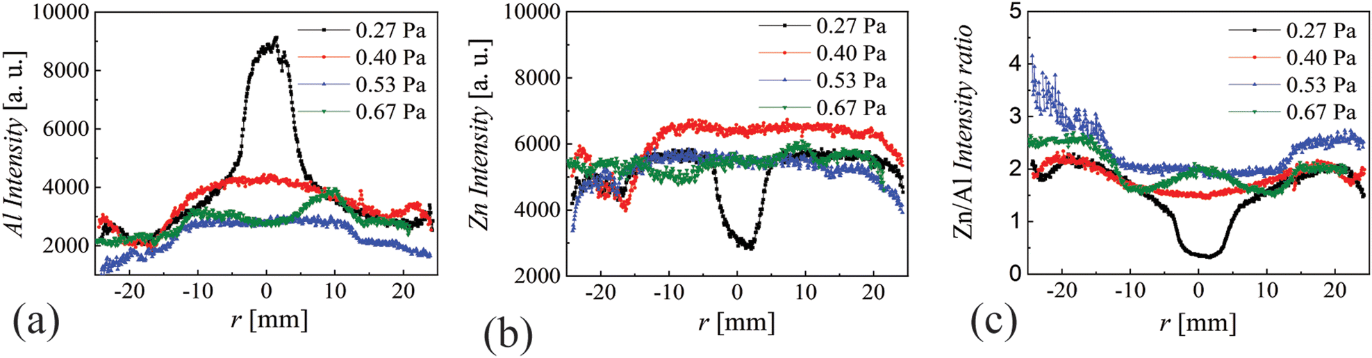
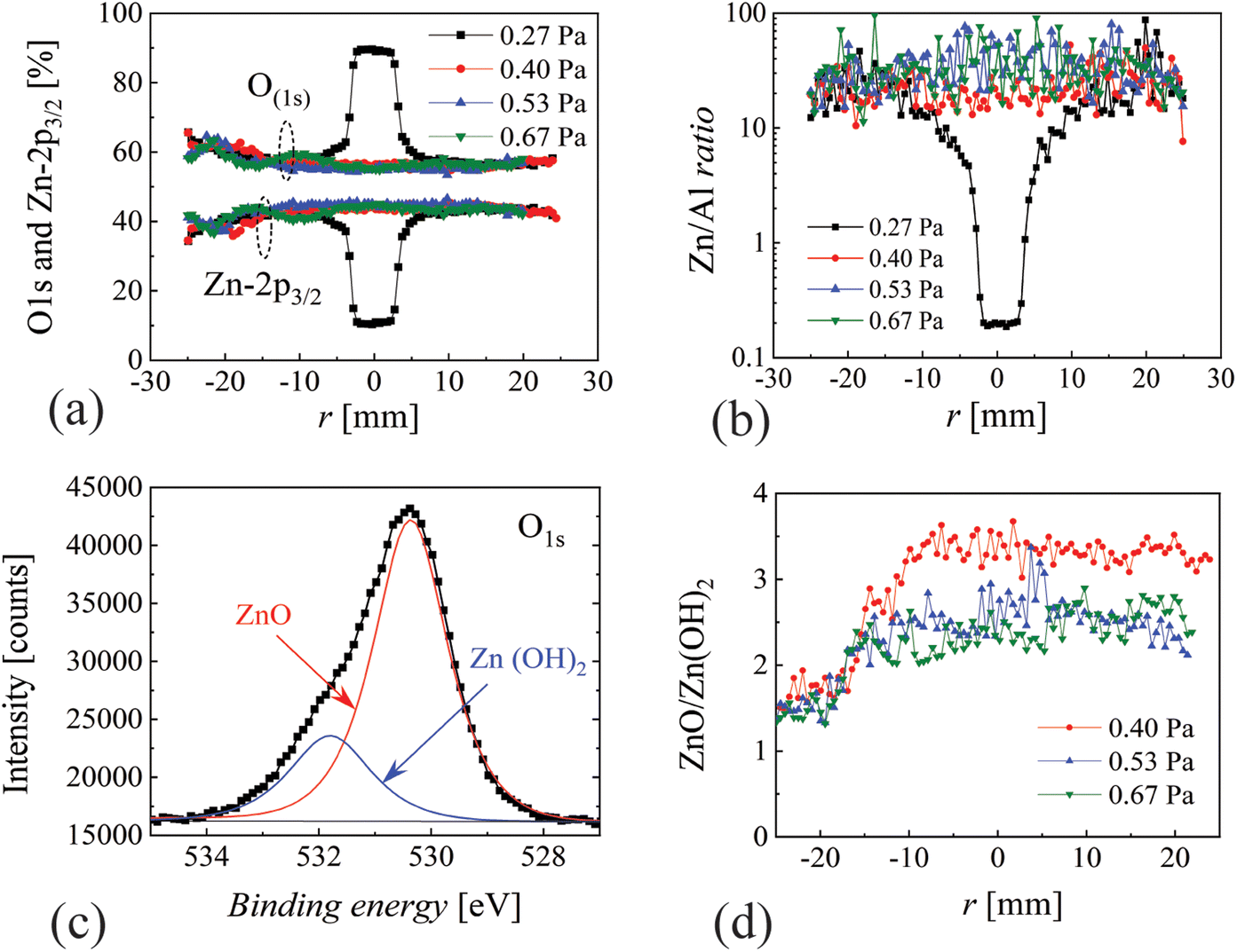
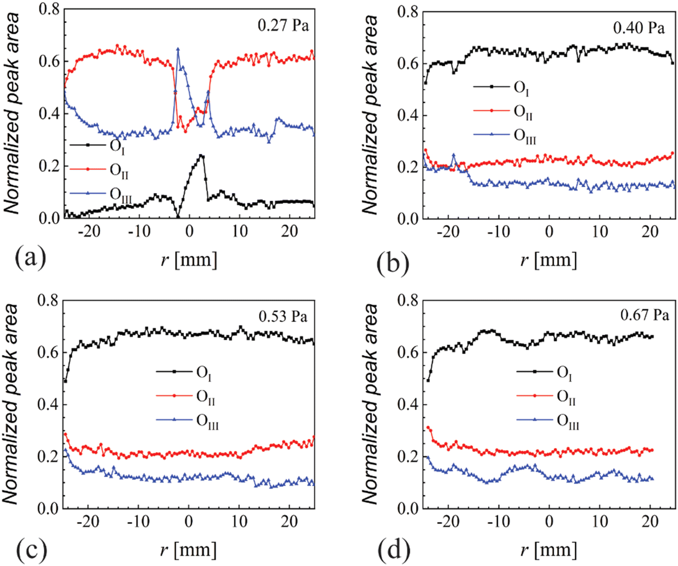
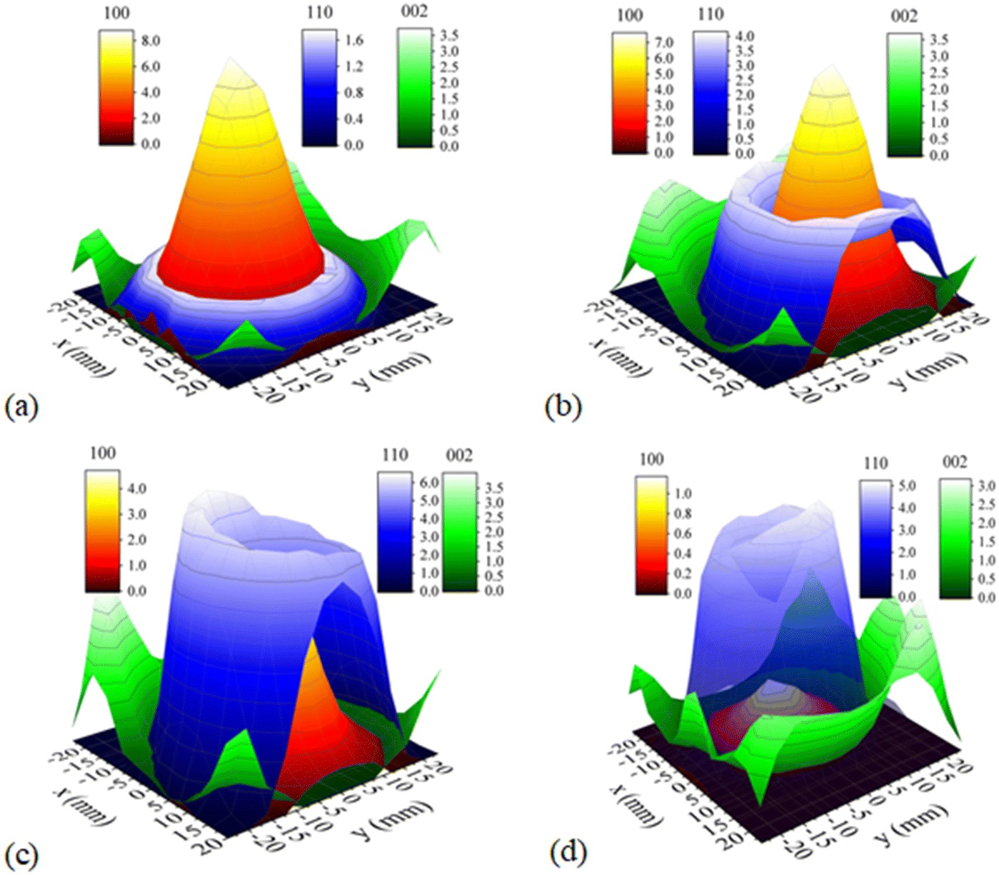
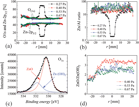
The spatial distributions of the sheet resistance, film thickness and resistivity measured on 10 × 50 mm2 substrates at different pressures are shown in Fig. 2(a–c), respectively. This type of variation has been presented and discussed very recently and can be summarized as follows.31–33 The discharge is in the plume-like mode at 0.27 Pa with a difference of almost two orders of magnitude between the sheet resistance values at r = 0 and |r| ≅ 17 mm and a high re-sputtering rate for |r| < 10 mm (see the reduced thin film thickness). By reducing the target-to-substrate distance or increasing the RF discharge power, the intense re-sputtering observed at 0.27 Pa becomes directly visible as a complete thin film removal for |r| < 5 mm.31 Increasing the pressure to only 0.4 Pa brings the discharge in an intermediate state with much uniform values for the sheet resistance, thickness, and resistivity but yet a significant re-sputtering rate for |r| < 10 mm. At 0.53 and 0.67 Pa, the discharge is in the magnetron sputtering mode with sheet resistance and resistivity profiles correlated with the erosion track on the target surface and significantly higher film thickness for |r| < 10 mm (above 350 nm). The sheet resistance and resistivity exhibit, as expected,31 more than two orders of magnitude differences at 0.67 Pa (see for example between values around |r| ≅ 12 mm and r < −20 mm). For completing the physical characterization, the spatial distributions of the average transmittance (400 to 700 nm) and energy band gap at 0.4 and 0.67 Pa are shown in Fig. 2(d and e), respectively. While the transmittance shows a very shallow correlation with the erosion tracks at 0.67 Pa, there is no noticeable link at 0.4 Pa where the transmittance is more than 5% higher than at 0.67 Pa. However, the band gap (measured from Tauc plot) shows a very clear correlation with the erosion track and significantly higher values (above 3.3 eV) much closer to the theoretical values of AZO at 0.4 Pa. Noticeably, the band gap at 0.67 Pa increases from 3.05 eV at r = −12 mm to 3.4 eV at r = −25 mm, locations that also correspond to lowest resistivity values (see Fig. 2(c)). It is obvious that such a remarkable evolution within a very narrow pressure range offers a unique opportunity to perform the analytical characterization in order to correlate the plasma role and behavior with the physical and chemical parameters of AZO thin films. For this purpose, the same samples were used to perform time-of-flight secondary ion mass spectrometry (TOF-SIMS) and XPS analyses. To avoid the possible physical interference of the measured points by the two methods, the measurements by each technique were performed 1.5 mm apart with respect to a symmetry line along the 50 mm long sample. Al, Zn and Zn/Al intensity ratios by TOF-SIMS are presented in Fig. 3(a–c), respectively. While the spatial distributions of Al and Zn intensity correlates to some extent with sheet resistance and resistivity values presented in Fig. 2, the correlation of Zn/Al intensity ratio with resistivity values is remarkable. First of all, the central part with high re-sputtering at 0.27 Pa shows a noticeable deficit of Zn (Zn/Al intensity ratio below 0.5) that can be attributed to very different sputtering yields by energetic oxygen ions. For example, the sputtering yield as function of oxygen ion energy is presented in Fig. S1 (ESI†) including the Zn/Al yield ratio.57 The absolute value of the DC self-bias was below 150 V at all pressures and a fact that limits the negative oxygen ion to below 150 eV. For this energy range, the Zn/Al yield ratio exceeds 6 and consequently supports the assumption of the preferential depletion of Zn by ionic bombardment for |r| < 5 mm. Ion energy distribution functions measured during AZO deposition by magnetron sputtering in DC and RF operation modes revealed higher energies for DC than RF, reaching close to 500 eV26 where the Zn/Al yield ratio is still above 4. Since the yield ratio increases sharply by decreasing the ion energy below 75 eV, it further complicates the possibility to avoid Zn depletion in the deposited AZO films. The highly localized Al-rich region for |r| < 5 mm correlates very well with the plume-like plasma discharge mode at 0.27 Pa that have been detected with the dual thermal-electrostatic probe.33 The Zn/Al intensity ratio reached above 2.4 in Fig. 3(c) for r < −15 mm at both 0.53 Pa and 0.67 Pa where the resistivity was below 10−3 Ω cm. The most uniform Zn/Al intensity ratio values, around 2, were obtained for |r| < 15 mm at 0.40 and 0.53 Pa, corresponding to moderate resistivity values around 3 × 10⁻³ Ω cm. Measuring oxygen by the extremely sensitive TOF-SIMS technique is complicated due to the erroneous contribution of residual gas despite very low operation pressures. In this context, XPS being less sensitive to residual oxygen could give the needed complementary information. The spatial distributions of the O-1s and Zn-2p3/2 peaks obtained from XPS at different pressures measured for the same samples presented in Fig. 2 are shown in Fig. 4(a). The Zn depletion for |r| < 5 mm is again observed at 0.27 Pa and corresponds to a noticeably high contribution in the O-1s peak at the same location. The same pressures (0.53 and 0.67 Pa) exhibited higher O-1s and lower Zn-2p3/2 for z < −25 mm where the lower resistivity values have been measured. The Zn/Al ratios at all four pressures are shown in Fig. 4(b) and reveal a very strong Zn depletion for |r| < 5 mm, corresponding to the intense and preferential Zn re-sputtering at 0.27 Pa when the discharge is operating in the plume mode, in a very good correlation with TOF-SIMS measurements at 0.27 Pa presented in Fig. 3. However, while the Zn/Al intensity ratio measured by the very sensitive TOF-SIMS method correlates very well with the resistivity profile at all pressures, and the corresponding less sensitive XPS obtained ratios were very noisy at pressures above 0.28 Pa, with no detectable correlation with resistivity. The O1s peak shape suggests that it is composed of ZnO and Zn(OH)2 contributions as presented in Fig. 4(c). The spatial distribution of the ZnO/Zn(OH)2 ratio at different pressures is presented in Fig. 4(d) and shows a pronounced decrease to below 1.5 for r < −17 mm where the lowest resistivity values were measured (see Fig. 2(c)). Due to the very low level of Al doping (only 2%), the Al+3 peak at 78 eV exhibited a low but a detectable intensity. A common way to analyze O-1s was to deconvolute it in three components: 530.15 ± 0.15 eV (OI) related to the amount of oxygen atoms in a fully oxidized stoichiometric surrounding, 531.25 ± 0.25 eV (OII) related to variations in the concentration of oxygen vacancies, and 532.40 ± 0.15 eV (OIII) related to loosely bound oxygen on the surface as presented in Fig. 5 at different pressures. Except for the noticeable localized variation for |r| < 5 mm at 0.27 Pa, linked to the plume-like plasma, there is no obvious correlation with spatial profiles presented in Fig. 2 except for higher values of OIII at the expense of OI for r < −25 mm at 0.53 and 0.67 Pa where the lowest resistivity values were measured. In order to take advantage of the full 2D capability of XRD, pairs of 10 × 50 and 50 × 50 mm2 soda lime glass samples were deposited at 0.33, 0.40, 0.47 and 0.53 Pa. The 10 × 50 mm2 samples were used to measure the sheath resistance while the large samples of 50 × 50 mm2 were used to record the 2D XRD spectra. The sheet resistance values are presented in Fig. S2 (ESI†) and show, despite the very narrow pressure range, a pronounced variation for |r| < 10 mm related to the transition from a plume discharge to a magnetron discharge, also connected with intense re-sputtering at lower pressures (0.33 and 0.40 Pa). It is important to specify that the samples at 0.40 and 0.53 Pa are deposited under identical conditions compared to those presented in Fig. 2(a). The 2D mapping on the four 50 × 50 mm2 samples of (100), (110), and (002) peaks is shown in Fig. 6(a–d), respectively. The correlation of the different zones of the discharge (central, erosion track and edge) with the (100), (110) and (200) peaks, respectively, is remarkable. Moreover, the XRD results correlate very well with the corresponding resistivity values and the Zn/Al intensity ratios obtained by TOF-SIMS. Low resistivity AZO requires the promotion of the c-plane (002) Wurtzite orientation while the m-plane (110) orientation is desired for applications requiring the anisotropic electrical
and mechanical properties such as signal processing and sensors.58 In an attempt to control the texture orientation, Takayanagi et al.59 used the energetic negative oxygen ions to promote the (110) orientation and the best results were achieved at regions that correlated with the erosion track, which is in very good correlation with the results presented in Fig. 6. The central part of the samples, dominated by the (100) orientation, is strongly correlated with Zn depletion by preferential sputtering as presented in Fig. 3(c). The very narrow range of pressure exhibiting the sharp transition from a dominant (100) orientation at 0.33 Pa to (110) at 0.53 Pa can only be explained by the observed transition from the plume-like discharge to the magnetron discharge, where the main plasma parameters, such as the plasma potential, electron temperature, and plasma density, presents a clear transition that strongly correlates with the self-bias variation included in Fig. 1(c).33
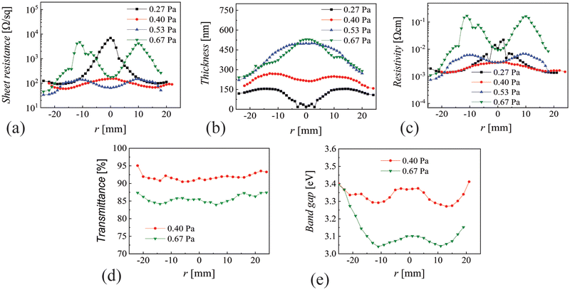 |
| | Fig. 2 Spatial distributions of the (a) sheet resistance, (b) film thickness, (c) resistivity, (d) average transmittance and (e) band gap at different discharge pressures of thin films deposited over 30 min at a 30 W RF power. | |
 |
| | Fig. 3 Spatial distributions of the (a) Al intensity, (b) Zn intensity and (c) Zn/Al intensity ratio measured by TOF-SIMS on the same samples presented in Fig. 2. | |
 |
| | Fig. 4 XPS investigation at different pressures presenting: (a) spatial distributions of O-1s and Zn-2p3/2 peaks, (b) the spatial distribution of the Zn/Al ratio, (c) O-1s deconvolution accounting for ZnO and Zn(OH)2 contributions, and (d) the spatial distribution of the ZnO/Zn(OH)2 ratio. | |
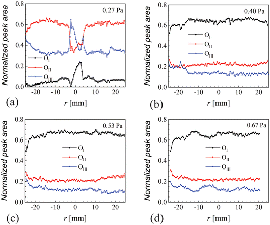 |
| | Fig. 5 Spatial distributions of the O-1s deconvolution in OI, OII and OIII contributions at (a) 0.27 Pa, (b) 0.40 Pa, (c) = 0.53 Pa and (d) 0.67 Pa, respectively. | |
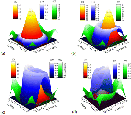 |
| | Fig. 6 2D-XRD patterns for (100), (110) and (002) orientations at (a) 0.33, (b) 0.40, (c) 0.47 and (d) 0.53 Pa, respectively. | |
4. Conclusion
The properties of AZO thin films have been investigated in a very narrow range of pressures (0.27 to 0.67 Pa) corresponding to the minimum values of the DC self-bias that controls the energy of negative oxygen ions assisting the film growth and providing the lowest resistivity values over a substrate comparable in size with the sputtering target. The TOF-SIMS acquired spatial distribution of the individual Al and Zn intensities was found to correlate to some extent with the sheet resistance and resistivity. However, the Zn/Al intensity ratio was found to correlate extremely well with the resistivity values. This was attributed to the central part having a higher degree of re-sputtering at 0.27 and 0.40 Pa, which is evident from a noticeable deficit of Zn, attributed to a very different sputtering yield by energetic oxygen ions with respect to Al. No obvious correlation was found between the high-resolution XPS spectra (Zn-2p3/2 and O-1s) and the sheet resistance and resistivity, except for higher values of loosely bound oxygen on the surface at the expense of the oxygen atoms in fully oxidized stoichiometric surroundings (r < −25 mm at 0.53 and 0.67 Pa) where the lowest resistivity values were observed. Moreover, the deconvolution of the O-1s peak in three components revealed a noticeable variation only at the sample center at 0.27 Pa, with very flat profiles at higher pressures, a fact that will need further consideration. The Zn/Al ratio by XPS revealed a significant Zn depletion only for −10 < r < 10 mm at 0.27 Pa. At the same time, no detectable correlation could be observed with the same ratio by neither TOF-SIMS nor the resistivity profiles. In contrast, 2D XRD profiles exhibited an excellent correlation with the sheet resistance, resistivity and Zn/Al ratio by TOF-SIMS, resembling the main regions describing the magnetron plasma discharge, respectively: (i) the central part, dominant at low pressures (plume-like discharge) and associated with 100 orientation, (ii) the erosion-track-mirroring, associated with the 110 orientation and the magnetron discharge, which accentuates with the discharge pressure increase, and finally, (iii) the edge or shadow region, associated with the 002 orientation, where the lowest resistivity values are typically reported for very small sample areas with respect to the sputtering target. Since the highest Zn/Al ratios (above 2.5) by TOF-SIMS correlate with the lowest resistivity values and the dominant 002 orientation, it is reasonable to conclude that the high depletion of Zn (Zn/Al < 1.5) observed at the sample center for 0.27 favors the 100 orientation and the mild depletion (Zn/Al < 2.5) associated with the erosion track favors the 110 orientation. So far, special attention was devoted to find an appropriate level of Al doping. However, the present work presents evidence that Zn depletion needs to be compensated or avoided. This aspect points at the need to develop improved physical deposition methods for uniform and low resistivity AZO thin film deposition that could avoid or compensate the intrinsic particularities of the magnetron sputtering discharge.
Author contributions
E. S. designed and directed the research; K. N. performed the TOF-SIMS and XPS characterization and P. N. performed the XRD characterization; E.S. performed the additional experiments and wrote the manuscript, which was discussed and amended by K. N. and P. N.
Conflicts of interest
The authors declare no conflicts of interest.
Acknowledgements
This work was partially supported by the SmartCoating project 6151-00011B, financed by the Innovation Fund Denmark.
References
- K. Ellmer, Nat. Photonics, 2012, 6, 809–817 CrossRef CAS.
- C. G. Granqvist, Sol. Energy Mater. Sol. Cells, 2007, 91, 1529–1598 CrossRef CAS.
- T. Minami, Semicond. Sci. Technol., 2005, 20, S35–S44 CrossRef CAS.
- M. B. Cortie, M. D. Arnold and V. J. Keast, Adv. Mater., 2020, 32, 1–8 CrossRef PubMed.
- S. Seo, S. Jeong, C. Bae, N. G. Park and H. Shin, Adv. Mater., 2018, 30, 1–8 Search PubMed.
- K. Hagedorn, W. Li, Q. Liang, S. Dilger, M. Noebels, M. R. Wagner, J. S. Reparaz, A. Dollinger, J. Schmedt Auf Der Günne, T. Dekorsy, L. Schmidt-Mende and S. Polarz, Adv. Funct. Mater., 2016, 26, 3424–3437 CrossRef CAS.
- M. Gaceur, S. Ben Dkhil, D. Duché, F. Bencheikh, J. J. Simon, L. Escoubas, M. Mansour, A. Guerrero, G. Garcia-Belmonte, X. Liu, M. Fahlman, W. Dachraoui, A. K. Diallo, C. Videlot-Ackermann, O. Margeat and J. Ackermann, Adv. Funct. Mater., 2016, 26, 243–253 CrossRef CAS.
- T. Minami, H. Nanto and S. Takata, Appl. Phys. Lett., 1982, 41, 958–960 CrossRef CAS.
- K. Ellmer, J. Phys. D: Appl. Phys., 2000, 33, R17–R32 CrossRef CAS.
- Z. Ghorannevis, E. Akbarnejad, A. Salar Elahi and M. Ghoranneviss, J. Cryst. Growth, 2016, 447, 62–66 CrossRef CAS.
- K. H. Patel and S. K. Rawal, Thin Solid Films, 2016, 620, 182–187 CrossRef CAS.
- C. Zubizarreta, E. G-Berasategui, I. Ciarsolo, J. Barriga, D. Gaspar, R. Martins and E. Fortunato, Appl. Surf. Sci., 2016, 380, 218–222 CrossRef CAS.
- A. Sreedhar, J. H. Kwon, J. Yi and J. S. Gwag, Ceram. Int., 2016, 42, 14456–14462 CrossRef CAS.
- M. Mickan, U. Helmersson, H. Rinnert, J. Ghanbaja, D. Muller and D. Horwat, Sol. Energy Mater. Sol. Cells, 2016, 157, 742–749 CrossRef CAS.
- B. Zhao, L. dan Tang, B. Wang, B. wu Liu and J. Heng Feng, J. Mater. Sci.: Mater. Electron., 2016, 27, 10320–10324 CrossRef CAS.
- V. Devi, M. Kumar, D. K. Shukla, R. J. Choudhary, D. M. Phase, R. Kumar and B. C. Joshi, Superlattices Microstruct., 2015, 83, 431–438 CrossRef CAS.
- J. Nomoto, H. Makino and T. Yamamoto, J. Appl. Phys., 2015, 117, 045304 CrossRef.
- F. Fumagalli, J. Martí-Rujas and F. Di Fonzo, Thin Solid Films, 2014, 569, 44–51 CrossRef CAS.
- N. Evcimen Duygulu, A. O. Kodolbas and A. Ekerim, J. Cryst. Growth, 2014, 394, 116–125 CrossRef CAS.
- L. Wen, B. B. Sahu, H. R. Kim and J. G. Han, Appl. Surf. Sci., 2019, 473, 649–656 CrossRef CAS.
- B. B. Sahu, J. G. Han, M. Hori and K. Takeda, J. Appl. Phys., 2015, 117, 023301 CrossRef.
- J. T. Gudmundsson, Plasma Sources Sci. Technol., 2020, 29, 113001 CrossRef CAS.
- T. Ishijima, K. Goto, N. Ohshima, K. Kinoshita and H. Toyoda, Jpn. J. Appl. Phys., 2009, 48, 116004 CrossRef.
- P. Pokorný, M. Mišina, J. Bulíř, J. Lančok, P. Fitl, J. Musil and M. Novotný, Plasma Process. Polym., 2011, 8, 459–464 CrossRef.
- S. Scribbins, M. Bowes and J. W. Bradley, J. Phys. D: Appl. Phys., 2013, 46, 045203, DOI:10.1088/0022-3727/46/4/045203.
- A. Bikowski, T. Welzel and K. Ellmer, Appl. Phys. Lett., 2013, 102, 10–14 CrossRef.
- J. Y. Tsao, S. Chowdhury, M. A. Hollis, D. Jena, N. M. Johnson, K. A. Jones, R. J. Kaplar, S. Rajan, C. G. Van de Walle, E. Bellotti, C. L. Chua, R. Collazo, M. E. Coltrin, J. A. Cooper, K. R. Evans, S. Graham, T. A. Grotjohn, E. R. Heller, M. Higashiwaki, M. S. Islam, P. W. Juodawlkis, M. A. Khan, A. D. Koehler, J. H. Leach, U. K. Mishra, R. J. Nemanich, R. C. N. Pilawa-Podgurski, J. B. Shealy, Z. Sitar, M. J. Tadjer, A. F. Witulski, M. Wraback and J. A. Simmons, Adv. Electron. Mater., 2018, 4, 1600501 CrossRef.
- J. Meyer, S. Hamwi, M. Kröger, W. Kowalsky, T. Riedl and A. Kahn, Adv. Mater., 2012, 24, 5408–5427 CrossRef CAS PubMed.
- K. Ellmer and T. Welzel, J. Mater. Res., 2012, 27, 765–779 CrossRef CAS.
- Y. Sato, K. Ishihara, N. Oka and Y. Shigesato, J. Vac. Sci. Technol., A, 2010, 28, 895–900 CrossRef CAS.
- E. Stamate, Nanomaterials, 2020, 10, 14 CrossRef CAS PubMed.
- E. Stamate, Surf. Coatings Technol., 2020, 402, 126306 CrossRef CAS.
- M.-A. Petrea and E. Stamate, Plasma Sources Sci. Technol., 2021, 30, 045002 CrossRef CAS.
- S. Khan and E. Stamate, Nanomaterials, 2022, 12, 1539 CrossRef CAS PubMed.
- C. Charpentier, P. Prod’homme, I. Maurin, M. Chaigneau and C. P. I. Roca, EPJ Photovoltaics, 2022, 2, 25002 CrossRef.
- L. Wen, B. B. Sahu, H. R. Kim and J. G. Han, Appl. Surf. Sci., 2019, 473, 649–656 CrossRef CAS.
- M. Kumar, L. Wen, B. B. Sahu and J. G. Han, Appl. Phys. Lett., 2015, 106, 1–6 Search PubMed.
- H. Dondapati, K. Santiago and A. K. Pradhan, J. Appl. Phys., 2013, 114, 143506 CrossRef.
- C. Lung, M. Toma, M. Pop, D. Marconi and A. Pop, J. Alloys Compd., 2017, 725, 1238–1243 CrossRef CAS.
- D. Miao, S. Jiang, H. Zhao, S. Shang and Z. Chen, J. Alloys Compd., 2014, 616, 26–31 CrossRef CAS.
- H. Li, L. K. Schirra, J. Shim, H. Cheun, B. Kippelen, O. L. A. Monti and J. L. Bredas, Chem. Mater., 2012, 24, 3044–3055 CrossRef CAS.
- M. Chaves, R. Ramos, E. Martins, E. C. Rangel, N. C. Da Cruz, S. F. Durrant and J. R. R. Bortoleto, Mater. Res., 2019, 22, e20180665 CrossRef CAS.
- A. Crovetto, T. S. Ottsen, E. Stamate, D. Kjær, J. Schou and O. Hansen, J. Phys. D: Appl. Phys., 2016, 49, 295101 CrossRef.
- D. K. Kim and H. B. Kim, J. Alloys Compd., 2011, 509, 421–425 CrossRef CAS.
- P. Misra, V. Ganeshan and N. Agrawal, J. Alloys Compd., 2017, 725, 60–68 CrossRef CAS.
- T. Prabhakar, L. Dai, L. Zhang, R. Yang, L. Li, T. Guo and Y. Yan, J. Appl. Phys., 2014, 115, 0–7 CrossRef CAS.
- H. M. Kim, C. H. Lee, S. Y. Shon and B. H. Kim, Appl. Surf. Sci., 2017, 421, 18–23 CrossRef CAS.
- S. H. Jeong and J. H. Boo, Thin Solid Films, 2004, 447–448, 105–110 CrossRef CAS.
- S. Y. Tsai, Y. M. Lu, J. J. Lu and M. H. Hon, Surf. Coat. Technol., 2006, 200, 3241–3244 CrossRef CAS.
- T. Tsuji and M. Hirohashi, Appl. Surf. Sci., 2000, 157, 47–51 CrossRef CAS.
- C. P. Liu, Z. H. Li, K. O. Egbo, C. K. Kwok, X. H. Lv, C. Y. Ho, Y. Wang and K. M. Yu, J. Phys.: Condens. Matter, 2021, 33, 465703 CrossRef CAS PubMed.
- R. Cebulla, R. Wendt and K. Ellmer, J. Appl. Phys., 1998, 83, 1087–1095 CrossRef CAS.
- B. Szyszka, Thin Solid Films, 1999, 351, 164–169 CrossRef CAS.
- B. P. Shantheyanda, V. O. Todi, K. B. Sundaram, A. Vijayakumar and I. Oladeji, J. Vac. Sci. Technol., A, 2011, 29, 051514 CrossRef.
- C. Charpentier, P. Prod’Homme and P. Roca i Cabarrocas, Thin Solid Films, 2013, 531, 424–429 CrossRef CAS.
- V. Tiron, L. Sirghi and G. Popa, Thin Solid Films, 2012, 520, 4305–4309 CrossRef CAS.
- N. Matsunami, Y. Yamamura, Y. Itikawa, N. Itoh, Y. Kazumata, S. Miyagawa, K. Morita, R. Shimizu and H. Tawara, At. Data Nucl. Data Tables, 1984, 31, 1–80 CrossRef CAS.
- W. R. Ali and M. Prasad, Sens. Actuators, A, 2020, 301, 111756 CrossRef CAS.
- S. Takayanagi, T. Yanagitani and M. Matsukawa, Appl. Phys. Lett., 2012, 101, 1–4 CrossRef.
|
| This journal is © The Royal Society of Chemistry 2022 |
Click here to see how this site uses Cookies. View our privacy policy here. 
 Open Access Article
 This Open Access Article is licensed under a Creative Commons Attribution-Non Commercial 3.0 Unported Licence
 a and
Eugen
Stamate
a and
Eugen
Stamate